Q8 QUIBBLE
I'VE SPOTTED TWO MINOR ‘RKV Car Amp ’ errors (TAA 1/89, p.21). In my schematic (p. 22) Q8 is labeled MJE253; it should be MJE243. Q8 is correct in the parts list. In the reference to IC1 (last sentence of text, p. 23) pin 16 should be pin 6.
RANDOLPH K. VIRAN Seattle, WA 98155
MOSFET vs. PULSE
A CONSTRUCTION NOTE on the 40W MOSFET Power Amplifier (TAA 2/88):
We all probably have an idea why our receiver can make a noise burst when someone switches on an electrical appliance in the house, even if it is only an incandescent light. The electric can opener can make quite a racket in the TV sound, too. Such radio frequency interference is so common we ignore it; un fortunately, for the receiver ’s MOS transistor these peaks of current or voltage (any pulse, even of sub-microsecond duration) can break down the gate oxide, leading to a failed device if the pulse can get to the MOS part.
K. E. Logan reported possible gate oxide failure mechanisms in his letter (TAA 3/88, p. 52), at which time I replied that circuit protection exists against such troubles. But protection is necessary against another mechanism-amplifier internal self-imposed failure-for which I offer an explanation and possible cures.
After I assembled several MOS power amplifiers, one power transistor failed occasionally, burning out the associated 0.51 ohm resistor, as well. The failures occurred in only one amplifier, which was in a 19- by 3- by 12-inch rack with the amplifier cards lying flat in the chassis and the heatsinks for the power transistors mounted on the rear chassis panel.
I then reviewed Mr. Logan ’s suggested zener clamp protection of the gates.
The zener solution cured my burnout failure, but I wanted to know the cause, not merely prevent what might be a symptom of some more complicated event, since the failure always happened to the same device and in only one of my amplifiers.
The transistor apparently failed when I turned on the unit, so I guessed the turn-on transient from the power line could in some way arrive at the critical spot. With a digital storage scope that could store and display the transient captured at the instant of turn-on, I studied the transistor ’s gate circuit layout and tuning and discovered the wiring harness was acting as an antenna, receiving a radiated pulse of energy able to take out the gate.
Figure 1 shows the signal at the AC power switch; this switch closure can be seen to bounce several times, and each time a response is seen at the receiving gate terminal. The relative polarities of each AC line surge and the resultant gate voltage transient are preserved through all three pulses. It is perhaps inevitable that some such event takes place during power-on. The amplitude of the received pulse is a matter of timing. When the AC line is switched on near the zero crossings of the 60Hz line, a small pulse occurs. Occasionally the switch closes near the peak of the 60Hz wave, the worst possible moment, with large radiated surges and large received pulses.
You may ask, why is the result only a few volts, and is this small signal a problem? Accidental tuning of the gate circuit or a very high transient on the power lines will cause a destructive pulse amplitude. Figure 2 shows a diagram of the gate circuit-an unterminated trans-mission line, with the circulating pulse current determined by the efficiency of the loop at the tuned frequency, as well as by the radiated energy at that frequency. It would be fortunate indeed if a test such as that in Fig. 1 were to show the very pulse that caused a breakdown. But it doesn ’t take much imagination to sup pose that a different resonant tuning of the gate loop, or longer wiring runs, could result in a pulse peak large enough to take out the gate, whose rating is 20V.
Figure 3 is a trace of the AC power line current on the same time scale as Fig. 1: this radiating event sends the interfering signal through the power line wiring to the gate. The rise-time of this particular pulse is about 10:8A per sec. This strong pulse is probably worsened by the use of a toroid power transformer. The square hysteresis characteristic of the core material of this type of transformer can re main partially magnetized at turn-off. If by chance the power switch closes in the opposite magnetic sense at the subsequent turn-on, there can be a worst-case current in-rush that generates these occasional large pulses. I mentioned this feature in my article; toroid power transformers can take out the fuse at turn-on, even though there is no fault in the system.
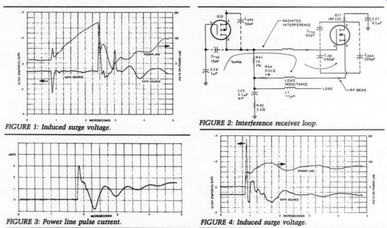
Fig. 1. Fig. 2. FIGURE 3: Power line pulse current. FIGURE 4: Induced surge voltage.
FIGURE
5: 12V zeners.
Figure 4 is a more common example, with a rather clean power-line voltage step from zero to + 100V, causing a sharp pulse with damped wavetrain recovery on the gate. The resonance is about 5MHz. I used a grid-dip meter to explore for resonances in the circuit. I found many small peaks and a rather efficient one at about 19MHz after I reworked the circuit; a lower tuned frequency was in effect before the rework.
Several possible solutions exist, each with pros and cons, depending on your particular circuit construction. You can shield the AC lines, bypass the switch contacts with an RC snubber network, or both. Other choices are to install an inrush-current limiter in the AC power lines, shorten and perhaps shield the leads connecting the amplifier circuit boards to the power transistors, or add a clamp network to the output transistors, most simply by a zener diode.
I reworked the affected amplifier, shortening the power transistor leads 50% by reducing about 16 inches of lead from board to heatsink to an 8 -inch run, which still allowed a neat wire route. I retested with the transient-capture oscilloscope and recorded pulse peaks at no more than a few volts. My amplifier has not experienced any further problems of this type.
The transient test, however, is not easy, since it requires special-purpose and high-tech equipment to see the actual pulse. Further, you never know whether you have actually found the worst case.
Although this method was successful, I prefer one that does not require fancy test equipment.
To eliminate the source of the problem, you must reduce the fast rise-time current occasionally seen on the power lines. An in-rush suppressor installed in the AC leads of the power supply circuit is simple and does not affect the amp ’s performance. You can use either a thermistor type of suppressor or a ‘hash ’ choke, such as is used in RF suppression in ham radio systems. I suggest specific parts below.
The suggested zener clamp method corrects the receiving end of the pulse pick-up problem. A happy consequence of using MOS devices is their operating bias of about +4V. This puts a gate-to-source clamp at an operating point considerably removed from zero bias, where zeners exhibit their largest junction capacitance. Also, in the amplifier design, the current from the driver stage does not supply a reverse drive to the output stage-it merely drops to a low of zero when turning the inactive side ‘off.’ Thus, you do not need to provide sym metric clamping; the normal reverse direction 0.6V clamping action of most zeners is appropriate. Since you require only about + 6V to at most + 8V of for ward drive at this circuit point, you can choose the clamp to go into operation at 12V or so with no effect on the circuit operation. A zener voltage of 12-20V is thus appropriate.
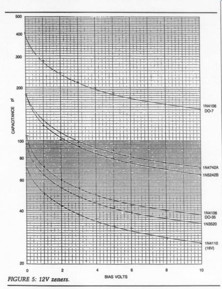
You must, however, consider the capacitance of the zener. Figure 5 shows the measured effective capacitance of several zeners. Notice the types in the DO-35 or DO-41 package seem to pro vide smaller capacitance than the larger DO-7. The capacitance varies with the bias voltage, essentially as the square root of voltage. This nonlinearity is added to the load on the driver stage, and can increase the generation of harmonics.
Worse, a zener can cause the circuit to become unstable, thus you must add it with care.
At least two sensible locations exist for a zener clamp. You can solder it onto the pads (already present on the card) for the gate and source leads to Q11 and Q12, which puts the clamp across R41 (see Fig. 2) and across the similar R42 of Q12 (not shown). This connection has potential problems-the clamp is applied to the wrong end of the antenna-cum-trans mission line, formed by the lead inductance and C_iss, as shown in Fig. 3, and may not be effective in clamping the received energy. Preferably, you can locate the clamp on the base pins of the power transistors, where it becomes a part of the heatsink subassembly. The zener then appears across C_iss.
A cautionary note: the zener possibly can act as an unfortunate termination of the ‘transmission-line ’ wiring, resulting in a destructive VHF oscillation. In the rework of the amplifier, I noted a high frequency parasitic oscillation appearing at about 160MHz. This can be mysterious if you don ’t have a very high-frequency oscilloscope for testing. The DC behavior of the amplifier can strangely wander, with the DC output becoming several hundred millivolts off zero for no apparent reason, which the superlative high-frequency gain of the MOS devices can sustain. The circuit drawing on page 14 of the original article shows the location of RF beads described in the text.
These beads do a wonderful, almost magical job of ridding the circuit of parasitic oscillations, and I strongly recommend them.
I offer the following construction rules in light of this experience:
1. Arrange the amplifier circuit cards following the diagram in Fig. 23¢c of the article, with the card ’s output edges facing the rear, so the power transistor leads to the heatsink are short, or;
2. Arrange the cards lying flat in a standard rack-style chassis so the input edges of the cards are toward one chassis side panel and the output edges are toward the center of the chassis. Run the power transistor leads down the center of the chassis to the rear, where they connect to the heat sinks. Run the amplifier input wires along the side panel of the chassis to the input connectors on the front or rear panels.
3. Arrange the 110V power wiring of a rack chassis installation along the opposite edge of the chassis from the amplifier card inputs, and perhaps hid den from view of the other wiring behind the transformer.
These lead-dress rules are an attempt to minimize transient energy crosstalk from the power lines to the amplifiers.
You may want to use one or more of the following circuit additions:
1. Install a current surge-limiter thermistor such as the Digi-Key KC014L in series with the AC power leads. A ‘hash ’ choke, such as the Digi-Key M-5240, may also serve this purpose.
Either requires appropriate insulation and mounting, since they involve the AC power line and may remain energized even when the power is switched off.
2. Install an RF snubber capacitor across the AC power switch contacts.
This capacitor should be rated at about 0.01 uF 250V AC, such as a Digi-Key P-4601.
3. Install 12-20V clamping zeners, described earlier. Types 1N4742A to 1N4747A are available in the DO-41 pack age from Digi-Key, and you can easily mount them in the available space. At +4V bias, these parts present about 90pF to the circuit for the 12V unit, lower for the higher voltage rating.
4. After reworking to whatever degree you require, and before powering up the circuit, temporarily reinstall the 100, 1W protection resistors I described in the test section of the original article. Follow that procedure again to ensure the amplifier is stable and performing as desired, then remove the safety resistors.
I did not suggest a noise specification for the MOS input transistors, since normally their noise performance is accept able in this circuit. If your system speaker efficiency is high, though, you may experience too much noise, which could actually be the result of a noisy Q1 or Q2 transistor. You can replace these input transistors with n-channel JFET units, such as the common replacement type NTE458 or a similar low-noise n channel JFET. If you do replace them, you must remove the clamp diode D3 (see complete schematic, TAA 3/88, p. 41), which will cause a circuit bias error if used with depletion-mode devices such as most JFETs. Substituting the JFETs will cause the operating voltage of the drain of transistor TR4 to change from about -3V as shown on the schematic to about + 1V to ground, depending on the particular Q1 and Q2 you use. This circuit modification has been built by several users, with the 458 transistor for Q1 and Q2, with good results. Clamp diodes D1 and D2 can remain in place with JFET input devices.
I hope these cautionary comments and discussion give you a better understanding of your circuit, so you will know how your creation actually performs. I believe something inventive and worthwhile has been made available for music listening enjoyment.
WILLIAM CHATER Ranchos Palos Verdes, CA 90274
-------------
… AND MOSFET PART II
WHILE COLLECTING THE COMPONENTS to build Chater ’s 40W Mosfet amp, Part II of his article arrived (TAA 3/88). Three errors I noted are: (1) R2 is shown as 100 k-O in the schematic on page 41 and as 330k in the parts list; (2) C1 is shown as 0.47uF in the schematic, but given as 0.15 uF in the parts list. According to my calculations, for an input time constant of 3Hz, C1 should be 1uF if R2 is 330 k-O (TAA 2/88, p.16); and (3) on the printed circuit board layout, one end of R2 does not seem to go to the ground track running through the amp-how does the low/high current ground get to it? I also have a question. Is the general printed circuit board layout critical to the operation of the amp? I ask this because I want to make a different layout (obviously adhering to good PC design rules).
Also, you can use cheaper output de vices, such as the IRF 520, which are electrically identical to the IRF 120, differing only in their pinouts and physical dimensions (plastic TO-220 cases).
Similarly, the IRF9213 could also be used in place of the IRF9210, but its electrical specs are slightly different.
MIKE ROSENSTEIN
Johannesburg, South Africa 2192
William Chater replies:
You are correct in your very careful attention to details of the parts list. The resolution is that either the parts list version or the schematic diagram version will work equally well. R2 is correctly 100k, but was 330k in TAA 3/88; C1 is correctly 0.47uF polypropylene, not 0.15uF; TR1, 3 and 5 are 2N2222, not 2N222; TR2 and 6 can be 2N2907A in stead of the rarer 2N3799 listed; and C31 can be 330pF polypropylene versus 300pF mica.
The problem arose when I made a change from the original 0.15uF and 330kf-ohm to a lower impedance, with R2 changed to 100k and C1 changed to 0.47uF. You will probably have noticed that either of these combinations has the same time constant, about 50 msec, which results in a lower frequency cutoff of 3.2Hz, the result of 0.5 pi times the time constant.
In the ground trace to the bottom end of R2, the missing conductor is on the reverse side of the card. The plated through hole style of card construction sees to it that there is a connection to this trace. If you make cards without plated-through holes, please be careful to follow up on the need for through-the card connections at several points in the circuit-the bottom end of R2 is just one example. As you insert the parts in the card, check whether you must solder both solder side and component side pads to ensure circuit completion.
Your question about the MOS parts is quite good. Surely the IRF520 is the equal of the IRF120 electrically, and will do just as well. The smaller unit, however, may have a lesser heat-sinking capability. If it is adequately heat-sinked I would not hesitate to use it. The servo connection in the circuit (Al through A4) will fix the operating current at about 200mA DC: you can adjust it downward (by increasing the resistance of R35 from 1.5M to about 2M, for instance), which should reduce the operating point of the IRF520s to about three-fourths the present value.
This would lower the heating of the out put stage by a few watts. You will want to test this new condition in listening tests and by making the tests suggested in the article to assure yourself the sound is not affected.
The board layout is not critical; I have successfully taken many liberties with the circuit in experiments. You should of course locate the RF bypass capacitors close to the same points and include RF beads. The IRFF9210 p-channel is a 200V unit, chosen to improve the character istic of the device at the circuit ’s operating voltages, even though the circuit does not apply anything like 200V. A substitution of the 150V IRFF9213 is perfectly acceptable; I would expect the difference to be indistinguishable.
Good luck with your project!
Note: Two new boards are available from Old Colony Sound Lab, PO Box 243, Peterborough, NH 03458 (603) 924-6371:
PCBX-3 Chater 40W MOSFET Amp 4.25 x 6.75 [2,3:88] Two-sided, one channel. Each $24.
PCBX-3A Chater Amp Power Supply 3.5 x 6.5 [2,3:88] Each $14.
DC 100 MODS
ANY ARTICLE ON A COMPLEX subject such as an amplifier must pass quickly over some of the finer design details to fit in a space less than that of a book. The Borbely DC 100 (TAA 1/84) seems to be a well-designed amplifier, especially in light of its fully complementary input section and balanced drivers.
Wanting to know more about the de sign and piqued by the author ’s reference to ‘the fully symmetrical DC circuit first tried here in June 1982, but abandoned ... because it looked too expensive/complicated...,’ I followed up on the design ’s origins. I found articles in Wireless World by Mr. Borbely (March 1983) and earlier articles by J. L. Linsley Hood (June-August 1982) on MOSFET amplifiers.
I could not locate Mr. Borbely ’s 1982 design and wonder whether his 1983 WW design is a simplified version or essentially the same. It seems his 1984 TAA de sign descends from these earlier designs (Mr. Hood ’s included).
In the WW design Mr. Borbely details the driver circuit, calling for ‘good linearity at high levels’ and noting the need for higher current availability to drive the MOSFETs. His solution is a cascode configuration, since the wide bandwidth will avoid transient overload.
In the TAA article he recommends either MOSFETs or bipolar devices for the driver stage output, but he prefers the MOSFETs since they have less phase shift (wider bandwidth) at frequencies of interest. He states that using the MOSFETs as source (emitter) followers adds ‘nonlinearity to the circuit, but it also increases the open-loop gain, which, converted to feedback, corrects the non linearity.’ Now my questions: would it make more sense to drive the MOSFET driver stage with the cascode-configured pre driver circuit of 1983, to eliminate as much of the nonlinearity as possible? It seems best not to rely on feedback.
Would it be possible to use the MOSFET within the cascode circuit? Clearly, the bipolar substitutes could be used this way.
Why was the cascode circuit abandoned in the Servo 100? Was the main consideration parts cost or diminishing returns in terms of specifications/performance?! Which brings me to my next problem: performance.
All the amplifiers-the DC 100, Servo 100, Borbely WW design and Hood design-have virtually identical specifications, power and distortion. The DC/ Servo 100 specs are marginally better and faster with lower distortion.
I would expect the DC 100 to outperform the Servo 100; the input section should be faster, quieter and better balanced, at least. Given the obvious differences in input circuitry, is the driver/output section the limiting factor in the amplifier ’s performance? The output section consists of four MOSFETs per channel, to drive 120W in to 8-ohm, and 140W into 4-ohm. Why is the power into 4-Ohm not twice the power into 8-Ohm (as with most transistor amplifiers)? Is this amplifier current limited by the power supply and output device ratings? At full output, one side of the amplifier ’s four output devices is ideally driven fully on and the other fully cut off. Full power represents one-half the full supply voltage presented to the load through one side of the amplifier ’s output section.
A quick check of Ohm ’s law shows that for the specified 40V RMS power supply voltage, at 4-Ohm a current of 10A would be drawn across that load, which would correspond to 400W (assuming a ‘0 ’ resistance ‘on ’ condition). We might expect, however, to find 240W in to 4-Ohm, given the 120 at 8, in our amplifier.
More realistically, given the no-load supply voltage of 50V (per side), the RMS voltage becomes 35V; taking into ac count the on condition of the MOSFETs and the series resistors, a load of (worse case) less than 1 Ohm appears in series with the load of 8-Ohm, for a total of, say, 8.850.
Ohm ’s law gives us I = 3.95A and 130W dissipated by the 8-Ohm load, which drops about 8W across the MOSFETS, in addition.
Now, at 4-Ohm the total series resistance of the string is 4.85 Ohm (approximately). At the same 35V RMS there is 7.216A drawn for a total dissipation of 252.5W. With the series resistance of the circuit equal to 17.5% of the total resistance, the dissipation shoots up to 44W. A quick look at the I3j- Vg curves for the 2SK134 shows that at 35V one unit can handle about 3.0A, two will get us 6.0A. This is still less power handling capability than we need for the 4-Ohm load, at full supply voltage, if the supply will deliver 6A at 35V RMS.
Now, what about those pesky 2 loads found in electrostatics, ribbons and other assorted speakers? At 2 Ohm ‘I’ rises to a whopping 12A, and total power to a room-warming 430W. The devices in this case will dissipate 30% of the power, or 128W, whereas the load itself sees only 302W.
It is clear that two MOSFETs will not handle 12A of current anywhere near the full supply voltage of 50V peak. At less than 15V two MOSFETs could do it.
Why not use four MOSFET per supply rail, for a total of eight devices per channel? This would add considerable head room for low impedance loads. An added benefit would be greater apparent efficiency, since now a lower ‘on ’ resistance would be available.
In another issue, couldn ’t the additional drive current needed to overcome the gate capacitance be solved by increasing the current in the driver output device? A larger driver MOSFET device might be needed to handle the increased current. Of course, a higher current power supply also would be a good idea.
Borbely ’s grounding methods for two amplifiers and one or two supplies is also puzzling. Why use a 10 ohm resistor from in put ground to ground of only one amplifier?
RANDALL BRADLEY
Hannacroix, NY 12087
Erno Borbely replies:
I didn ’t publish my 1982 design because I never finished the article. After Wireless World published the Linsley-Hood design, the editor delayed my 1983 design for more than a year. I revised the text to point out differences in the approach, but the design was not altered.
My TAA designs of 1984 followed my ideas from the 60W TAA design, not those of the WW article.
So much for history. Your question about the driver stage is valid; I selected the emitter/source follower simply as a convenience to be able to drive the in put capacitance of two or more pairs of the output MOSFETs. Although the article mentions only two pairs, I have been using anything from two to four pairs for different applications. In fact, I redesigned my DC 100 with this in mind and the amp works with up to six pairs for very low impedance loads. This de sign is called DC 100A (look for the schematic in an upcoming ‘Audio Aids ’). I have also added a cascode stage in the in put to alleviate limited breakdown volt age on the input transistors and improve linearity. This design does not imply that you can ’t use the WW a with more output devices, it is simply a different approach.
The output is less than double in 4-ohm because of the limiting diodes at the in put of the MOSFETs and the current capability of the power supply, both of which can be overcome. Using the larger Hitachi devices, as indicated on the DC 100A schematic, you can increase the voltage of the zener diodes and see a significant increase in output power in low-impedance loads. Naturally, you also have to increase your power supply. Optimum quiescent current has been found to be 200-250mA per pair of output devices, but feel free to experiment; you may have a different load than I have.
One word of caution: don ’t forget to pro vide proper cooling for your output devices when you are running them with this high quiescent current.
The grounding scheme with a 10 ohm resistor from one channel is meant to break up a ground loop between the preamp and the power amp, and may not be needed in your case. Since this is not a production type device, it doesn ’t necessarily give all details in terms of mechanical design; it merely suggests some possibilities.
SERVO 100 OUTPUT
REGARDING ERNO BORBELY ’S Servo 100 amp (TAA 1/84, p. 7) and increasing the number of output devices beyond the number originally specified, what is the maximum number I can parallel from each rail per channel? Can I go to six? I know that the driver stage is looking in to a fair amount of capacitance as origin ally designed and I do not want to overload it.
Also, do I increase the damping factor as I increase the number of such devices?
LES WINTER New York, NY 10003
Contributing Editor Erno Borbely replies:
Yes, you can increase the number of devices on the Servo 100, but I must admit I only tested it with up to four pairs.
However, I have tested my new amp de sign, the DC 100A, with up to six pairs, which should work very well with low impedance loads. Yes, you do increase the damping factor, but eventually it will be limited by the tweeter saver at the output.
Optimum quiescent current per pair is approximately 200mA, but feel free to experiment with this. Naturally, you will need a lot of heatsinking and a very big power supply to handle such current.
[Please see Mr. Borbely ’s reply to Randall Bradley, this issue.-Ed.]
Borbely DC 100 Supply
I am working as a aerospace design engineer in El Segundo, California, and find your articles educational even for us technical types. I must admit, though, that I would like to see more design information. For instance, after reading Mr. Borbely’s fantastic articles on both the Servo 100 and DC 100 amps, I wonder why he did not use the third pin on the LM336. I know the pin ’s function, and maybe it is not needed, but I think this option should at least be mentioned. Also, why does he use a resistor to separate the input ground from the power supply ground? I believe I know why, but again, I think this should be revealed in the design discussion.
Please do not misunderstand me; I very much enjoyed Mr. Borbely ’s articles. I was so impressed with his careful designs I bought two DC 100 kits. I applaud Mr.
Borbely for taking time to relay his design procedures, and TAA for sharing such talent.
EDWARD AHO, Santa Monica, CA 90405
[Please see Mr. Borbely ’s replies to Les Winter and Randall Bradley in this issue.-Ed.|
UPSETTING EDITORIAL
NORMALLY, I ACCEPT the content of your publication at face value in areas where your philosophy is in opposition to certain values which I hold in high esteem.
However, in issue 2/88, the Editorial states: ‘Audio is among the least demanding of the electronic disciplines,’ and then proceeds to elaborate on the techniques of material selection to achieve the desired quality reproduction we all endeavor to achieve. In my interpretation, I find the editorial to be greatly contradictory.
From personal experience, I know the design and construction of true quality audio equipment is one of the most demanding electronic disciplines. Furthermore, these demands extend to the areas of mechanical packaging and certainly to the areas associated with selection of passive components such as resistors, capacitors, and wire, to enumerate only a few. Many excellent electrical designs are ‘trashed ’ through poor mechanical layout even though component selection is excellent. In my estimation, nothing relating to audio equipment is easily accomplished. Indeed, most in stances of ‘happenstance ’ drive the performance away from the desired excellence.
Possibly you meant that the ‘mystique’ of high-end audio design is not limited to the regime of a few gifted de signers. If this was your intent, I heartily
recommend that you expand upon this concept in future editorials, supplemented with technical articles pertaining to packaging concepts and passive component selection.
K.E. LOGAN
Altamonte Springs, FL 32714
The Editor replies:
Although Mr. Logan is obviously a highly qualified and experienced engineer, I still maintain my belief regarding audio ’s relative place in the scale of engineering complexity. I agree wholeheartedly that it is more demanding than generally perceived, but so are other disciplines.
Also see:
A SIMPLE HIGH-QUALITY CD OUTPUT AMP, By Jan Didden
AC SENSING CONTROL, By LB. Dalzell
BOOK REVIEWS, Gary Galo and Rod Rees