
By J. A. "Sam" Wilson, CET
A second look at NAND gates brings the surprise of two different NAND formulas, and two different NOR formulas, along with a method of transposing formulas correctly. The characteristics of NOR latches are explained, also five troubleshooting questions are asked and answered.
NAND Gate Revisited
A Nebraska reader/technician called me last March asking for an explanation of this NAND-gate statement that appeared on page 54 of the February Electronic Servicing: "The math symbol should be read NOT A AND B equals L.
It is important that the overbar reach across both letters without a break," The inquiry is welcome because it gives me the opportunity of making some important points important points about digital circuits.
Probably the best way of explaining the statement is to carry both conditions (A x B= L, and A x B =L) through to the end. The first formula actually means that the overall AND function is negated at the output, while the second one calls for each individual input to be negated (inverted) before it reaches the AND gate.
We'll try both formulas, and show the results.

Figure 1 An AND gate followed by a NOT gate becomes a NAND. The math formula
for AND gates is read, "A AND B = L." The NOT gate at the output
negates that so it reads, "NOT A AND B = L." As shown in the drawing,
the overbar should cover both letters and the expression which is in between.
(It might be more clear written "NOT (A AND B) = L.")

Figure 2 Inverting both inputs of an AND gate does not produce a NAND gate
(notice the differences in the truth tables). Instead, it is another way
to construct a NOR gate. The formula is read, "NOT A AND NOT B = L.
Remember: NOT A AND B = L isn't the same as NOT A AND NOT B = L.
Inverted AND output an AND gate with the output inverted is shown in Figure 1, along with the truth table. Notice that the output state in the "L" column is obtained by inverting the A x B column of the AND.
All conditions are satisfied, so inverting the output of an AND gate DOES form a NAND gate, which has the same formula as in the February article.
Inverted AND inputs? In Figure 2, both the A and B inputs are inverted separately, giving A and B inputs to the AND gate. A glance at the inputs and the final output column reveals that the combination logic does NOT form a NAND gate.
Therefore, inverting the inputs of an AND gate does NOT produce a NAND! These two sets of facts prove that A x B=L is not the same as A x B = L. Remember, with combi national logic, only the A and B inputs and the L output states are important to the type of gate.
If you memorized the truth tables of the various gates as we discussed them during the past months, you are in for a surprise. The logic circuit and truth table in Figure 2 actually forms a NOR gate! However, the A x B = L NOR formula is different from the A + B = L NOR formula given in February.
This will be explained later.
Avoid NOR Errors A similar situation exists with NOR logic made from OR and NOT gates. The NOR math expression A + B = L is not the same as A + B = L.
Figure 3 shows a NOR gate constructed by feeding the output of an OR gate through an inverter.
The truth table verifies that the combinational logic circuit is a NOR, with a formula of A + B = L.
In the same way, Figure 4 shows a digital circuit formed by inverting both the A and B inputs to an OR gate. The output has the formula A + = L, which compared to the output formula for the NOR gate in Figure 3, proves that inverting the inputs of an OR gate does NOT give the same results as inverting the output of an OR.
The truth table in Figure 4 proves the digital circuit is not a NOR, but is a NAND! However, the A + = L formula is different from the NAND formula given last February OM3c = L).
These facts bring up two interesting points: (1) changing the overbar from a continuous line over the entire input to two individual overbars, produces a different gate; and (2) there must be more than one formula for each gate.
How else can we account for two NAND formulas and two formulas for NOR?
Conversion By DeMorgan's Laws
Because the A-x ri = L NAND formula of Figure 1 equals the A + B = L NAND formula of Figure 4, it follows that A x B = A + R.
Also, the NOR formulas of Figure 2 and Figure 3 give us the combined formula A x = A + B. These assumptions can be proven by an application of DeMorgan's Laws.
DeMorgan's Laws are very important for working problems in Boolean Algebra, and for showing that basic gates can be combined to obtain a desired output.
Figure 3 A NOR gate can be constructed by an OR gate whose output is inverted with a NOT. The formula is read, "NOT A OR B = L." (Try thinking of it as "NOT (A OR B) = L.")
Figure 4 Inverting both inputs or an OR gate does not produce a NOR gate.
(Compare the truth tables of Figure 3 and Figure 4.) The formula is read, "NOT A OR NOT B = L." Compare only the two inputs and the output columns of the truth tables in Figures 1, 2, 3 and 4. This combinational logic produces a NAND gate. However, the formula is not the same as the one previously given for NANDs. DeMorgan's Law will clarify the situation.

Figure 5 Using either the NOR gates of (A), or the NAND gates of (B), how
can you connect several gates to con struct one NAND gate?

Figure 6 This is a hint for answering Troubleshooting question #1.

Figure 7 Using either the NOR gates of (A), or the NAND gates of (B), how
can you connect sever al gates to construct a NOR gate?
------------Chart 1 Here is a chart with many helpful digital facts compiled tor easy reference. Refer to it as you answer the questions and work the experiments.
NOTES: In digit logic, the x and + signs NEVER mean "times" and "plus”.
The x sign is read AND, and the + sign is read OR.
An overbar negates (inverts state) whatever is under it. For example, A X B means NCT A AND B.
DeMorgan's Laws
In a digital-logic math expression, the overbar a ways can be broken it you also change the sign of the expression. Also, a broken overbar can be made continuous if you charge the sign of the expression.

Figure 8 DeMorgan's Law states that a continuous bar over the entire A and/or
B input expression can be changed to two separate bars over the individual
A and B input letters, by simultaneously changing the sign of the expression.
Also, individual overbars of the A and B inputs can be changed to one continuous
bar over both, by changing the sign of the expression.

Figure 9 A double overbar equals no bars.
Troubleshooting question #1
Using the integrated-circuit packages of Figure 5, how can you connect the pins to con struct a NAND gate? Hint: the output of a NOR gate is A + B. If this output is inverted, as shown in Figure 6, the gate is an OR.
(Answers to the trouble shooting questions are given at the end of this article.)
Troubleshooting question #2 Using the integrated-circuit packages of Figure 7, how can you connect the pins to con struct a NOR circuit?
DeMorgan's Laws simplified
John Merriner, CET, a California friend, gave me this simple rule for remembering DeMorgan's Laws: In digital-logic math expressions, the overbar always can be broken, if you also change the sign of the expression.
Using this easy-to-remember rule, it's possible to simplify some types of circuits, such as the one in Figure 8. The output is:
A x = L For the first step, break the overbar and change the sign of the operator:
X + E = L
Now, a double overbar is similar to a double negative in the English language. If we say, "You can't not go," it means, "You can go." In digital language, a "NOT NOT A" is the same as an "A." This is illustrated by the circuitry in Figure 9.
Chart
Chart 1 summarizes many gate formulas and other important material.
A New Symbol?
Several inquiries have been received about the industrial symbol in Figure 12, page 53, of the February article. The normally-closed contact was not correctly drawn. (A capacitor symbol was used by mistake.) The correct illustration is shown in Figure 10.
NOR Electronic Model
A request has been received for an electronic discrete model for a NOR gate (models were shown for AND, OR, NOT, and NAND).
Figure 11 is a NOR gate using two transistors.
When both switches are open, both transistors are cut off, there is no current through the collector resistor, and the output voltage at L is high.
Closing either or both switches provides forward bias to one or both transistors, thus producing saturation. This is a low-resistance short at the L output, so the output has logic 0.
All such electronic models are given only to help your understanding of the principles. Actual IC versions are not constructed that way. Integrated-circuit technology produces greatly improved bipolar gates. And CMOS gates are made using MOSFETs.

Figure 10
The normally-closed contact in Figure 12 page 53 of the February ELECTRONIC SERVICING was in correctly drawn. This contact is correct for an industrial schematic.

Figure 11
This is an electronic model of a NOR gate, constructed with discrete components. Either or both switches in high state produces a low output.

Figure 12
The schematic at the top is a latch circuit, constructed with two NOR gates. The inputs are criss-crossed so the package symbol is the same for both NAND and NOR latches.

Figure 13
These are the four steps for switching a NOR latch from low output to high, and then back to low again.
NOR Latches
Previously, the NAND latch was discussed. It also is called an RS flip-flop or a bounceless switch.
During the quiescent period of a NAND flip-flop, the R and S inputs both have highs. The flip-flop condition is changed from high to low by momentarily switching the R input to low (zero volts). And, it is changed from low to high by momentarily switching the S terminal to low (zero volts).
A latch can be made also with NOR gates. It, too, is called an RS flip-flop and a bounceless switch.
As shown in Figure 12, the input leads are crossed to place the set and reset terminals in the standard location for flip-flops.
For a NOR latch, the S and R input terminals both are held at logic-level zero during the quiescent period. To switch the flip-flop, the proper input terminal is switched momentarily to logic 1 (high). Note: the two inputs should never be switched to logic 1 at the same time.
Troubleshooting question #3 Is the latch of Figure 12 in the high condition, or in the low condition? Switching NOR latches Figure 13 gives some switching information for NOR latches.
During step 1, the latch is in the low condition, and the two inputs have lows, which is the quiescent condition for NORs.
For step 2, the S input is switched to, logic 1. (A NOR latch is switched by changing the proper input terminal from logic 0 to logic 1.) The stepping voltage for switching is equivalent to the leading (rising) edge of a square wave.
Therefore, NOR flip-flops normally are switched by the leading edge of an input pulse. By contrast, NAND flip-flops normally are switched at the trailing (falling) edge of an input pulse. These are important points that you should memorize.
Flip-flops of the TTL logic family usually are made with NANDs, while flip-flops of the CMOS logic family usually are made with NORs. Therefore, TTL flip-flops switch during the leading edge of input pulses, while CMOS flip-flops switch on the trailing edge of input pulses.
When the S terminal in step 2 of Figure 13 is switched to logic 1, the inputs to NOR #2 becomes 1 and 0.
(The previous levels are shown in parentheses.) The 0 output of NOR #2 is delivered to the input of NOR #1, making two logic 0 inputs for NOR #1, and this causes the output to switch to logic level 1. Note that the flip-flop has been switched from low to high by the leading edge of the input signal at the S terminal.
During step #3 the logic level at input terminal S has been returned to 0. Again, the NOR flip-flop is in the quiescent condition, but with a high-output condition.
For step #4 of Figure 13, the NOR flip-flop has been switched to a low condition by the leading edge of a positive pulse at terminal R.
When the pulse returns to logic 0, the flip-flop will remain in the low (quiescent) condition. The flip-flop has been taken through four steps, and now is in the original condition.
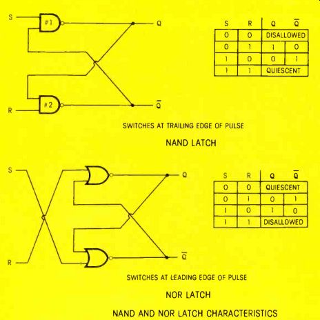
Figure 14 NAND AND NOR LATCH CHARACTERISTICS

Figure 15 This is one way of making a NAND from four NOR gates.

Figure 16 The circuit of Figure 15 can be drawn this way. Two NOTs feed
a NOR, thus forming an AND, then the final NOT changes it to a NAND.

Figure 17 Here is one way of wiring four NANDs to produce a NOR.

Figure 18 This is the circuit of Figure 17. Two NOTs and a NAND become an
OR, and the final NOT charges it to a NOR
Troubleshooting question #4
In a NOR latch circuit, the R input terminal is stuck in a logic 1 condition. Will the latch be stuck in a low (logic 0) condition?
NAND And NOR Latch Truth Tables Figure 14 shows the conditions for quiescence and switching in NAND and NOR truth tables.
Troubleshooting Question #5
A CMOS NOR latch will operate with a power-supply voltage of only 5 volts. Is it okay to substitute a CMOS NOR-latch for a defective TTL NAND latch?
Experiments with latches will be illustrated next month.
Answers To Troubleshooting Questions
Answer #1. The NOR gates can be wired to make a NAND, as shown in Figure 15. Perhaps you used different NANDS for inverters, but the important thing is for inversion to occur at the inputs, and again at the NOR output (to produce an OR). Refer to Figure 16 for a simplified schematic.
Answer #2. Connect the NAND gates as shown in Figure 17 to construct a NOR. You can select different gates to be used as NOTs, but the final circuit should be similar to the one in Figure 18.
Answer #3. The NOR latch in Figure 12 is in the high condition (Q is 1, and 0 is 0). The output logic levels are the same for both high and low conditions of NAND and NOR latches.
Answer #4. A NOR latch with the R input terminal stuck at logic 1 will be stuck in the low condition only as long as the S terminal remains at logic level 0. If S is switched to high, the condition can't be determined, for operation with both inputs high is disallowed.
Answer #5. No, a CMOS NOR latch should not be substituted for a TTL NAND latch, because CMOS latches switch at the leading edge, while TTL latches switch at the trailing edge. (There are a few rare exceptions.) Also, CMOS latches, when operated at the TTL voltage of 5 volts, switch slower than TTL latches do.
(adapted from: Electronic Servicing magazine, May. 1978)
Next: The Basics of Industrial Electronics, Part 12
Prev:
Also see: Sam Wilson's Technical Notebook