(index locations on both: gammaelectronics.xyz and industrial-electronics.com)
A straightforward amplifier module for radios or hifi, which makes particularly efficient use of the supply voltage available.
- Andrew Armstrong
AUDIO AMPLIFIERS come in many sizes, from the multi-kilowatt PA jobs used at rock concerts, to tiny hearing aid amplifiers. It is a case of horses for courses This particular amplifier is between the two extremes, and is intended for use in small radio receivers.
It is intended as a mix-n-match module which can help constructors to design their own projects without having to design every single circuit block. There is little point in building something you can buy cheaply in the shops, so this is a little different.
There is an increasing trend for radio sets to operate on lower voltages. This is very sensible for the RF and IF parts of the circuit, which do not normally require a very high voltage to amplify a few millivolts of RF efficiently. (This is not so of some dual gate mosfets, which may require several volts' bias to work Well.) The poor old audio amplifier is not always quite so well suited, however. As everyone knows, the power which may be delivered to a particular load is proportional to the square of the voltage applied. A reduction from 9V to 6V as a battery voltage would seem to offer 44% of the power, if all else were equal. It isn't. of course, because a normal audio amplifier output can only swing to within about 1V5 of each supply rail. Thus, with batteries at nominal voltage, the reduction is from 6V peak to peak to 3V peak to peak, a cut to 25% power.
Using an 8R loudspeaker as a reference, this is a reduction from 375mW to 93mW.
There are many ways of getting round this problem. such as lower impedance loudspeakers, bridge connected power amplifiers, step-up loudspeaker transformers, or just plain higher voltages.
The design featured here can help with all these methods--it simply swings closer to the power supply rails than most designs. Since it is automatically biased to the midpoint of the supply rails, it always makes the best use of whatever power there is.
How It Works
The block diagram. Figure 1. is very simple. The important fact is that the output stage has gain, and can swing close to the supply rails. even though the op-amp output has a lesser swing. This output stage gain is illustrated by Figure 2, and is approximately given by the ratio of R1 to R2. The approximation is more accurate if the emitter current of 01 is a small proportion of the total chain current.
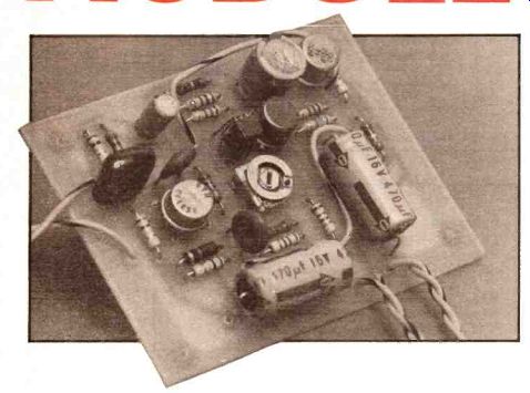
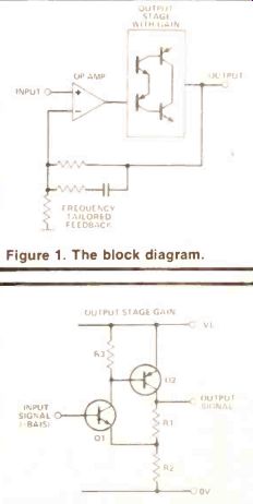
Figure 1. The block diagram. Figure 2. The output stage gain is roughly the ratio
of R1 to R2.
If the emitter current is negligible. then the reasoning is thus: the signal on the emitter of Q1 follows that on the base (but 0V6 lower). so the collector voltage of Q2 must be such as to permit this.
Given the resistors shown. the collector signal of Q2 is double the emitter signal of Q1. Gain = R2/(R1+R2) The feedback circuit is of some importance. The overall gain of the circuit must be high enough (ie the feedback must be low enough) that the circuit does not oscillate (a common problem with some types of op-amp circuits). Equally, there is no point in the amplifier providing high gain at frequencies which only the dog can hear, so a frequency rolloff has been provided to reduce the gain at above audible frequencies.
The Circuit In Detail
The input signal from the volume control is AC coupled via C1, which, in conjunction with R1 and R2, gives a low frequency rolloff with a 3dB point at 32Hz. No small transistor radio loud speakers will respond at this frequency.
The op-amp itself is a CA3130. The choice of this device was for two reasons--first it has a low power consumption, and second it uses an external compensation capacitor, so that the compensation can be made sufficient to discourage further any tendency to oscillation.
Stability And Gain
The voltage gain of the amplifier module is set by R6 and R7. It is (R7+R6)/R6 which is about 22. A rolloff starts at a frequency set by R7 and C7, approximately 23 kHz, and continues until the gain has fallen to about 6 at a frequency of 106kHz.
For oscillation to occur in a circuit with negative feedback, the phase shift round the loop (through all the stages of amplification, and back round via the feedback) must reach 180 degrees at a frequency at which the gain round the loop is at least 1. (If the gain is greater than 1, the circuit oscillates and clips until the average gain is 1.) The op-amp is compensated to be unity gain stable (ie with 100% feedback). Following this is a voltage gain of 2, and some extra phase shift.
Even at the highest frequencies.
however, the feedback is potted down by R6 and R8, ie by about 5:1. This may reasonably be estimated to give enough margin to take care of the extra x2 gain and bit of phase shift in the circuit, and preclude the possibility of making an RF oscillator transmitting on long-wave. The stability of the circuit is of course aided by the on-board decoupling capacitor, C6.
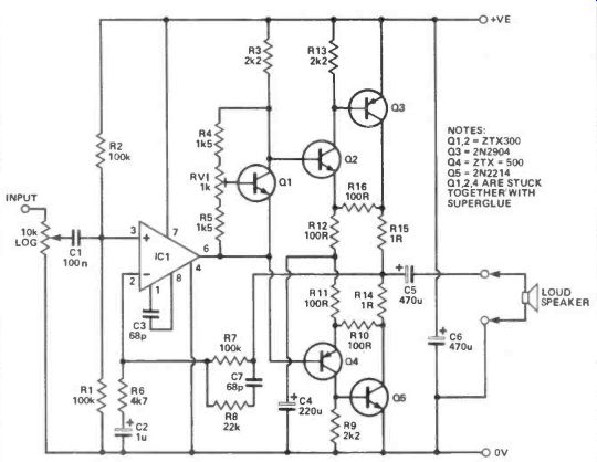
Figure 3. The circuit.
---------------
Parts list
RESISTORS
(All 0.25W 5% unless noted) R1, 2, 7 100k R3, 9, 13 2k2 R4, 5 1k5 R6 4k7 R8 22k R10, 11, 12, 16 100R R14 15 1R
POTENTIOMETERS
RV1 1k horiz preset
CAPACITORS
C1 100n
0.3" pin spacing eg. 04-10406 (Cirkit) C2 1u radial electro eg Cirkit 05-10508 C3, 7 68P ceramic C4 220u radial electro ,/N,Parts
05, 6 470u axial electro
NOTE: If a 3R loudspeaker is used, 1000u may be chosen for C5 to avoid restricting the low frequency performance too much.
NOTE: The voltage rating of all electrolytic capacitors must be above the power supply voltage chosen eg 6V supply (new battery may be 6V5) use 10V or greater rating.
SEMICONDUCTORS:
Q1.2 ZTX300
Q3 2N2904
Q4 ZTX500
Q5 2N2219
IC1 CA3130E
MISCELLANEOUS:
Any 10k log volume control, with or without switch as appropriate: any small loudspeaker: wire. solder etc.
---------------
The output stage, as already mentioned, provides a voltage gain. The first part of the output looks like a conventional symmetrical emitter follower, biased in the normal manner by Q1. Indeed, if Q3 and Q5 were omitted, and R12 and R11 reduced in value, the junction of R12 and R11 could conveniently form the output point. In this case, of course, the maximum output power would be reduced.
The addition of Q3 and Q5 provides an output gain as described before. This gain is completely symmetrical, and it means that the emitters of Q2 and Q4 would have to swing between points 1 V5 from either supply rail on a 6V supply, to enable the output collectors to reach the rails. Thus Q2 and Q4 have to do just about what a conventional amplifier can normally achieve. C4 decouples the junction of R11 and R12 to generate an artificial mid rail relative to which the output stage can provide its voltage gain.
Bias If the figures above are extrapolated back to the Op-Amp output pin, then, bearing in mind the bias effect of Q1, the output pin has to swing between 0V8 and 3V8 (again assuming a 6V supply). This it is perfectly capable of doing.
The quiescent current is set by the bias voltage on the bases of 02 and Q4, which it itself set by the collector to emitter voltage of Q1. For example, any increase in the current through Q3 will increase the voltage across R15. This, via R16, tends to switch off Q2, thus decreasing the drive which was turning on Q3.
Temperature stability is very important, because the quiescent current stabilizing effect detailed above is potted down by R12 and R16 on the positive side, and R11 and R10 on the negative side, so that any thermally induced change will have double the effect it would have in a more conventional output stage. To obtain good temperature stability, Q1, Q2. and Q4 are glued together with superglue. It was this requirement that led to the choice of transistor type--any old NPN and PNP transistors as long as they are in E line packages. It requires a degree of handicraft, and leads neatly on to. . . .
Construction
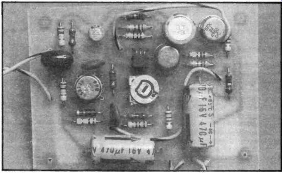
The module may be built on the PCB, or, by those who wish to do their own layout, on Veroboard. If it is built on Veroboard, then one of the three transistors to be glued together will probably have to be connected to different parts of the board by flexible wires. Don't let this deter you--the first version of this circuit, forming part of a small transistor radio, was built using this technique and it proved stable and reliable. It is still in use seven years later! The normal rules apply--it is best to start by fitting the resistors, then the capacitors, and the semiconductors last of all. Q1, Q2. and Q4 are a special problem--the leads of Q1 should point in the opposite direction to those of Q2 and Q4 when they are glued together.
This sandwich is illustrated in Figure 4.
To avoid confusion don't forget that the order of the connections on an E-line transistor is the reverse of that on a T092 device.
Q3 and Q5 are not shown provided with heatsinks--this should not be needed for most possible uses of this amplifier, but push on types may just be squeezed in if necessary. Alternatively, if higher power is needed, Q3 may be replaced by a BD132, and 04 by a BD131, bolted onto a heatsink. insulated with mica washers, and connected with insulated wires. If this scheme is carried out in order to get more output with damage. for example running on 12V as a car cassette booster, it may be advisable to replace R15 and R16 with OR47 types, so as not to waste too much power in these resistors. The same argument would apply to the use of a very low impedance loudspeaker, say 3R.
If this circuit is to be adapted to higher powers. there is one important point to remember. It is NOT short circuit proof, as many HiFi amplifiers are, so if you short the output and feed in a loud signal it will blow up. For this reason, any external wiring, for example to car loud speakers. should be carried out with due care to insulation so that a short cannot occur.
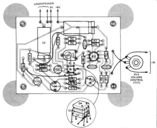
Figure 4. The component overlay. Note the 'sandwich' made up of Q1, Q2 and Q4 and pay close attention to the connections.
Testing
To test this module without risk of destruction, the best bet is to use a variable power supply. and to meter the current drawn. Turn up the power supply slowly, aiming for 6V, and stop if an alarming rise in consumption occurs.
Adjustment of VR1 should bring this under control--if it doesn't there is a fault. (If a variable power supply is not available, a 6V battery in series with a 10 R resistor is a fair substitute.) In the case of a fault. statistically, the most likely cause of problems is an error in the construction of the transistor sandwich (Q1. Q2. and Q4). Failing this, apply a voltage which does not cause alarming currents to flow. and check the voltage on the junction of R11 and R12, and on R14 and R15. Both these points should be at about half the supply voltage, and if either is not then suspect a short circuit.
When it all appears to work, adjust the quiescent current to about 3mA, and then connect a 'speaker and signal source and see how it sounds. In the unlikely event of any problems at this point re-check the midpoint voltages as above.
Now you just have to design the rest of your project ---- SHOP Nothing complicated here. just one or two things to note. To fit the PCB design, C1 must have 0.3 in pin spacing, so if you are not using the capacitor specified, check this before buying. C2 is less critical but 0.3 in spacing is preferred.
Q1, 2 and 4 must be built up into the transistor sandwich: for this reason, the most important thing about them is that they should have the E-line packages (ie flat-sided, with all the pins coming from one end of the device) as mentioned in the text.
The components for this module cost between £ (x 1.4 USD) 3 and £ (x 1.4 USD) 4 without the PCB No case is specified. of course
-------------
Also see: Link | --SHORT WAVE CONVERTER -- Allows you to use a medium-wave radio for short-wave reception.