Source: Radio Electronics--Electronic Experimenter's Handbook (1993)
by STEVEN D. SWIFT
Build this direct digital synthesizer, and generate low-distortion sine waves digitally.
HOW OFTEN HAVE YOU WISHED YOU had one of those fancy frequency generators that let you set your frequency accurately without having to fiddle with the uncalibrated tuning knob? Without a high-quality frequency counter and without nearly infinite patience, it is impossible to keep your audio oscillator on frequency without constant tweaking. If you eliminate the expensive extras, while retaining resolution and stability, you'll end up with the synthesizer project presented in this article.
While this synthesizer doesn't have the features of some very expensive products, it does provide 1-Hz resolution at over 500 kHz with crystal-controlled precision, all for less than $70. Once you add a suitable enclosure and power supply, you'll have a digital frequency synthesizer small enough to fit on even the messiest workbench. And it's perfect for providing that odd-ball frequency that your new project needs.
As the name implies, direct digital synthesis (DDS) is a method of frequency generation that uses digital methods rather than the traditional analog oscillator, phase-locked loop, or bank of crystals. The availability of fast digital circuits and D/A converters make this technology available to the average electronics enthusiast.
A review of trigonometry is important to the understanding of DDS before delving into the de tails of the electronics. Figure 1 shows a circle with a radius whose length is arbitrarily set to one. The radial line labeled R is allowed to rotate about the circle through an angle P. which will be referred to as the phase. Drawing a horizontal line from the tip of R until it intersects with the vertical axis defines the length S shown in the figure. As the radius, R, is allowed to make a complete rotation around the circle, the length of S takes on all values between +1 and-1, while P varies from 0 to 360 degrees. The length S is precisely the sine function of P, sin(P). shown in Fig. 2-a.
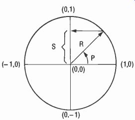
FIG. 1--THIS CIRCLE HAS A RADIUS whose length is arbitrarily set to one.
As R rotates around the circle, S takes on all values between 1 and 1.
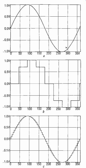
FIG. 2--THE LENGTHS, AS R ROTATES, Is the sine function of P (a). If we
make 8 equal steps around the circle, then we get the stepwise approximation
shown in b. If we make 64 steps, the approximation be comes closer to the
actual sine function (c).
If, rather than allowing R to rotate smoothly around the circle, we make 8 equal steps around the circle, then the values of S form the stepwise approximation shown in Fig. 2-b. As the number of steps are increased, the approximation becomes closer to the actual sine function, with Fig. 2-c showing the approximation for 64 steps. In practice, analog filtering is used to smooth out the steps, as we'll see in a minute.
From this simplified discussion, a method for generating a varying frequency can be de rived. Assume that each step occurs at a precisely determined instant, then by varying the step size the number of steps around the circle can be varied. The fewer the steps, the faster the complete circle is covered, hence the higher the frequency of the sine-wave approximation. Note that fewer steps means a coarser approximation to the actual sine function, with the output eventually reducing to a square wave, which points out one of the limits of this technique. All we need now is a circuit that will synchronize the variable-phase steps to a precision clock.
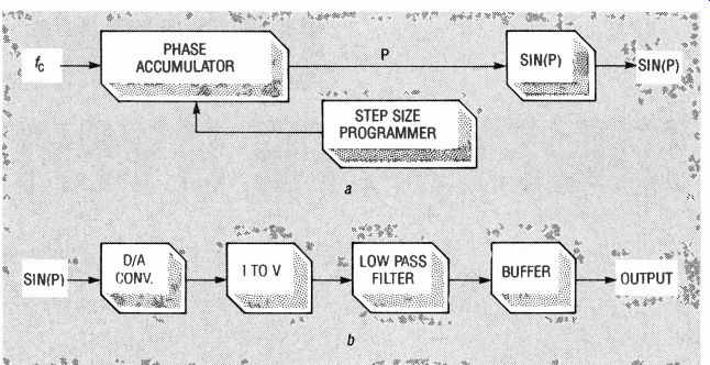
FIG. 3-BLOCK DIAGRAM of the phase accumulator and phase-to-sine converter
(a), and the block diagram of the digital-to-analog converter and output
stage (b).
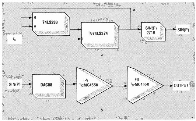
FIG. 4-PARTIAL SCHEMATIC of the phase accumulator (a) and the converter
and output stage (b).
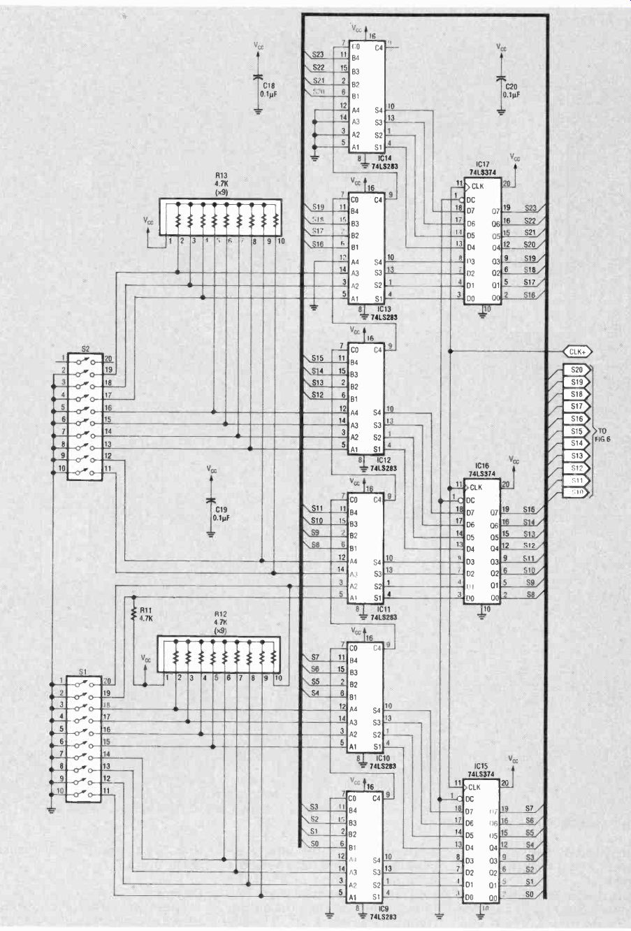
FIG. 5-HERE'S THE COMPLETE SCHEMATIC for the phase-accumulator circuitry.
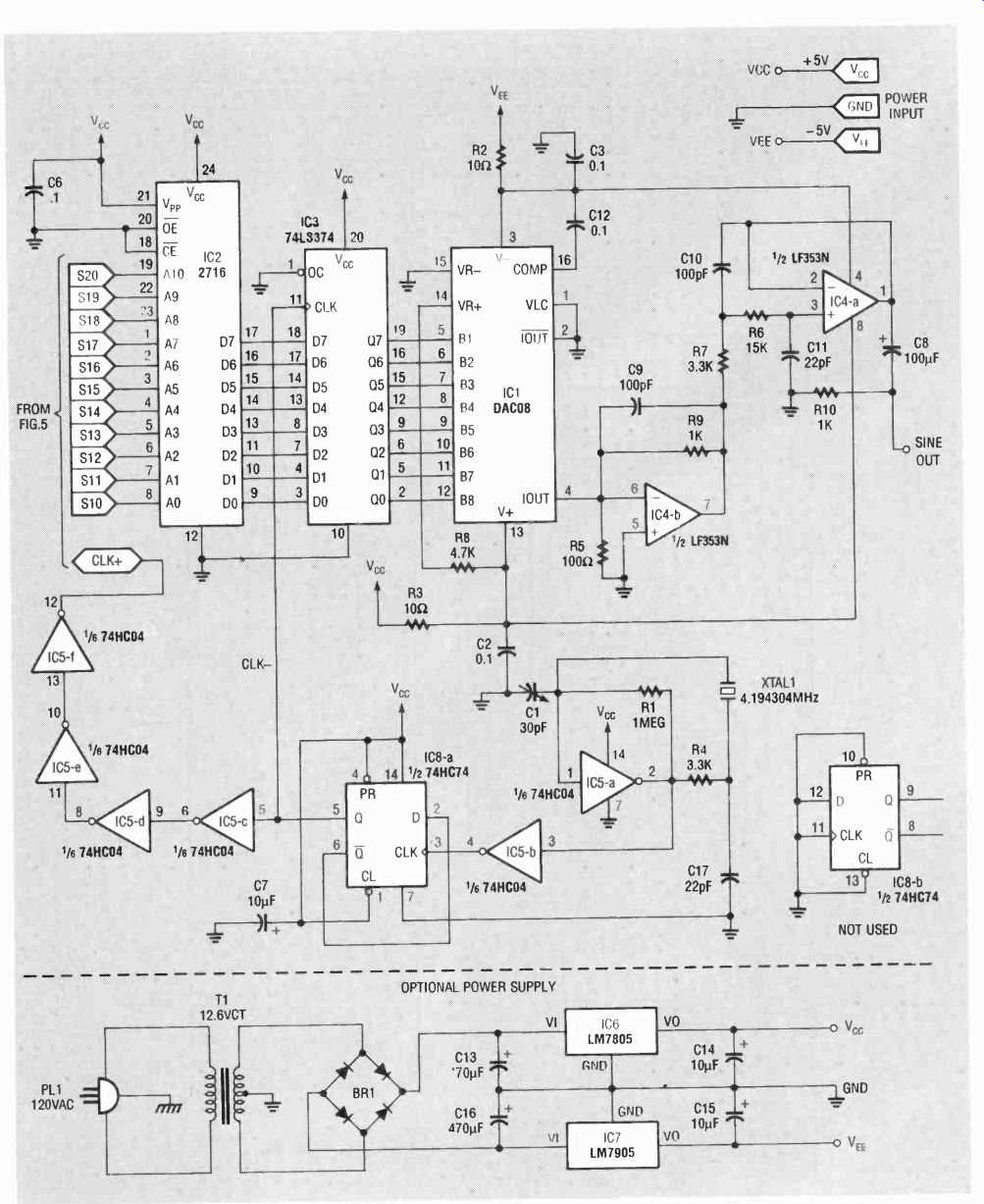
FIG. 6--THE SCHEMATIC for the analog section.
Figure 3-a shows a block diagram of the system. The block labeled Phase Accumulator repetitively adds the value set by the Step Size Programmer to the sum performing the function of stepping the radius (R) about the circle in equal phase increments.
The phase accumulator behaves like a simple counter, except that rather than incrementing its output by one on each clock pulse, the output advances by the value set by the step size programmer on each clock pulse. The block labeled SIN(P) converts the value stored in the phase accumulator to a sine amplitude approximation. The step size programmer is simply a bank of DIP switches, the phase accumulator is a series of cascaded 4-bit adders, and the SIN(P) block is a sine look-up table contained in an EPROM.
The digital data present at the output of the SIN(P) block must be converted to an analog voltage in order to be useful. A method for doing this is shown in Fig. 3 b, which consists of a D/A converter, filter, and output amplifier. The filter helps to smooth out the jagged steps in the sine approximation, while the output amplifier buffers the output of the D/A converter. In the actual implementation, the buffering and the filtering functions are combined.
The frequency resolution of a DDS system is set by the master clock frequency, fc, and the number of bits, N, in the phase accumulator. For the binary accumulator that we have here, the resolution is then fe/2N. If the step size programmer is set to a binary value, M, then the output frequency is M x fc/2N. The design presented here keeps M less than N/4 to minimize distortion at the output.
Circuitry
There are several manufacturers of complete integrated circuits that can perform the digital portion of the block diagram, but these parts are expensive and not readily available. Figure 4-a shows a partial schematic of the phase accumulator using components that are inexpensive and easy to get.
The complete phase accumulator consists of six 74LS283 4-bit adders, with their outputs latched by three 74LS374 octal D flip-flops. The outputs of the 74LS374's are fed back to the B inputs of the 74LS283, which forces the sum stored in the latches to be added to the value set by the switches on the A inputs. Since the 74LS374 stores data only at the positive edge of its clock input, the fact that the data presented to its inputs will be changing shortly after the clock causes no errors. The delay through the latch and adder guarantee glitch-free operation. At each clock pulse a new sum is present at the output of the latch. The output of each adder then stabilizes with the new sum allowing the cycle to re peat continuously. This sum rep resents the value P in the theoretical discussion, while the value set by the DIP switch represents the size of each phase step.
The sine-wave lookup table is contained within a single 2716 EPROM providing phase-to-amplitude conversion. Although 24 bits are available in the phase accumulator as implemented here, only 21 bits are used to maintain compatibility with readily avail able crystals. For those who wish to program their own EPROM, both a hex dump of the contents of the EPROM and an S-Record formatted hex dump for use with PROM programmers can be downloaded from the R-E BBS (516-293-2283, 1200, 2400, 8N1) in a file named DIGSYN.HEX. A programmed EPROM is available from the source shown in the parts list.
The data in the EPROM represents the values generated by the mathematical function 127.5(sin(2nP/2048-It/2)) truncated to 8-bits, with P taking on values from 0 to 2047, that is, the addresses of the EPROM. The formula offsets the sine function so that its value ranges from 0 to 255 as P ranges from 0 to 2047 and avoids negative values which would complicate the next stage.
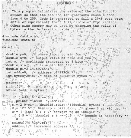
That matches the function to the 2716 EPROM with its 11-bit ad dress space and with its 8-bit output range. A C-program used to generate the values in the table is shown in Listing 1. Since the EPROM has only 11 address lines, only 11 lines from the accumulator are used in this application. The 8 bits at the output of the EPROM are a digital representation of the amplitude of the sine wave and must be converted to an analog voltage before being filtered and buffered.
Since simplicity and low-cost were design goals, the output of the EPROM is latched by another 74LS374, which allows the full clock period for the EPROM output to settle, permitting the use of inexpensive slow EPROM's.
The latch also guarantees a glitch-free input to the D/A converter section.
Figure 4-b shows the D/A converter circuitry. The D/A con version is accomplished using a DAC08 8-bit D/A converter (an MC1408 can be substituted with some loss in performance). The output of the converter is a current proportional to the digital value present on its 8-bit parallel input. The current is set by R8 to a maximum of 1.06 mA. The digital word presented to the D/A varies from 0 to 255, forcing the current output to vary from 0 to (255/256) x 1.06 mA. The current is then fed to op-amp IC4-b which converts it to a voltage that varies from 0 to approximately 1.0 volt. The complete schematic for the phase accumulator circuit is shown in Fig. 5, and the schematic for the analog section is shown in Fig. 6.
===========
LISTING 1
This program calculates the value of the sine function offset so that the 4th and 1st quadrants cause a code from 0 to 255. Code is generated to fill a 2048 byte prom (2716 or equivalent) for a full circle of 2*pi radians. Other size memory may be used by changing the value of bytes in the declaration table. */
==========
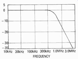
FIG. 7--THE RELATIVE RESPONSE of the filtering in the output stage. The
corner frequency is equal to 482 kHz. A high speed op-amp is required
to effectively filter the waveform.
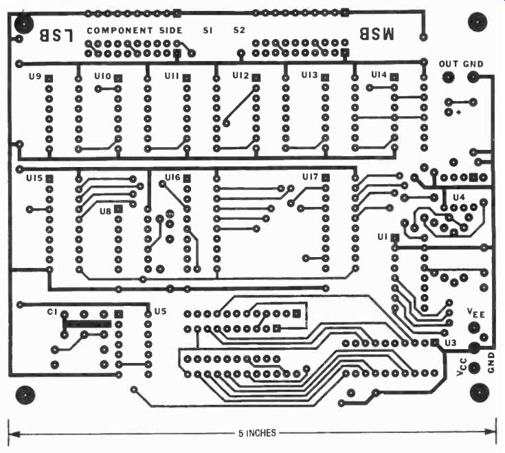
FOIL PATTERN for the component side of the digital synthesizer. FOIL PATTERN
for the solder side of the digital synthesizer.
First-order filtering is accomplished by C9 in this conversion stage. Op-amp IC4-a provides additional filtering to further smooth out the steps in the sine approximation. The output of this two-pole filter is AC-coupled to the output connection. Figure 7 shows the relative response of the filtering provided in the output stage. The corner frequency of the filter is set by the formula
fo = 1/(2nVR7 x C10 x R6 x C11)
which, for the values shown, is equal to 482 kHz. A high-speed op-amp is required in this stage to filter the waveform effectively.
The 4558 op-amp we used is a good compromise between performance and cost.
The clock for all functions is provided by a crystal oscillator running at 4.194304 MHz, which happens to be exactly the 22nd power of two. The clock is divided by two to provide the phase-accumulator clock and EPROM latch clock. Additional inverters are used as delay elements to en sure that the latches are clocked at precisely the right instant to prevent glitches. With the clock and timing as such, EPROM's with access times as slow as 475 ns can be used.
With 21 bits of the phase accumulator used and a clock frequency of 4.194304/2 MHz (fc), the output resolution is precisely 1 Hz. Since 19 bits are presented as the input to the phase accumulator by the DIP switch, the maximum output frequency is:
219x fe/221 = fe/4 = 524.288 kHz While a DDS system can approach fc/2, fc/4 was chosen as a maximum to limit the total distortion in the output waveform.
The top frequency is actually 1 Hz less than that because the maximum setting is 219-1 for a 19-bit binary input. The filter rolloff shown in Fig. 7 attenuates clock-related distortion by over 30 to 1.
========
PARTS LIST
All resistors are 1/4-watt, 5%.
R1-1 megohm R2, R3-10 ohms R4, R7-3300 ohms R5-100 ohms R6-15,000 ohms R8, R11-4700 ohms R9, R10-1000 ohms R12, R13-4700 ohms x 9, 10-pin SIP resistor
Capacitors
C1-5-30 uF trimmer C2, C3, C6, C12, C18-C20--0.1 uF, ceramic disc C4, C5-not used C7, C14, C15-10 uF 35 volts, electrolytic C8-100 uF, 16 volts, electrolytic C9, C10-100 pF, ceramic disc C11, C17-22 pF, ceramic disc C13, C16-470 uF, 16 volts, electrolytic (optional for power supply)
Semiconductors
IC1-DACO8CN 8-bit D/A converter IC2-2716 2K x 8-bit EPROM IC3, IC15-1C17-DM74LS374N octal latch IC4-LF353N dual op-amp IC5-MM74HCO4N hex CMOS inverter IC6-LM7805 +5-volt regulator (optional for power supply) IC7-LM7905-5-volt regulator (optional for power supply) IC8-MM74HC74AN dual D-type CMOS flip-flop IC9-1C14-DM74LS283N 4-bit adder BR1-1-amp bridge rectifier (optional for power supply)
Other components
XTAL1-4.194304 MHz crystal S1, S2-10-position DIP switch PL1-AC line cord (optional for power supply) T1-120VAC/12.6VAC transformer (optional for power supply)
Miscellaneous:
PC board, solder, case, mounting hardware, etc.
Note: The following items are available from NOVATECH IN STRUMENTS, INC., 1530 East lake Ave. E, Suite 303, Seattle, WA 98102 (206) 328-6902:
Complete kit of parts (except a case and the optional power-supply parts)-$69.95
Please add $5.00 shipping and handling. Washington State residents must add 8.2% sales tax.
===========
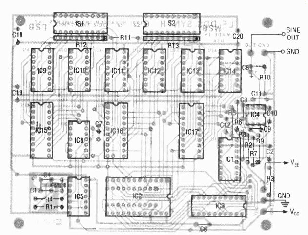
FIG. 8-PARTS-PLACEMENT DIAGRAM. Follow this diagram if you're using a PC
board.
The smaller IC outline beneath IC2 is for experimenting with a faster EPROM such as a 74S472 (see test).
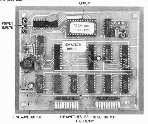
FIG. 9-THE COMPLETED UNIT. This compact PC board can easily be installed
in almost any kind of project case.
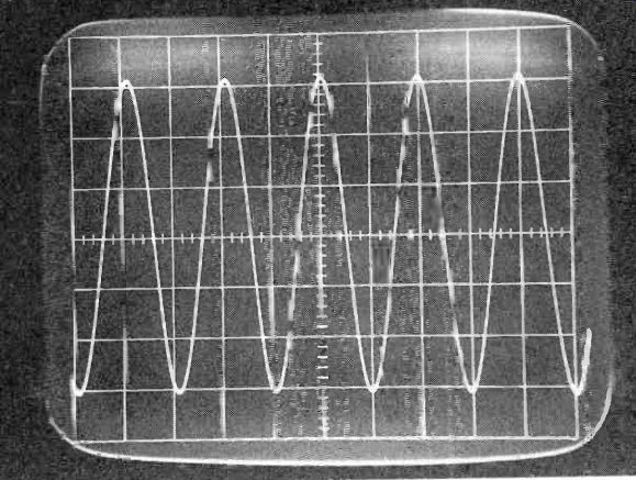
FIG. 10-0 INPUT OF THE AUTHOR'S PROTOTYPE at 100 kHz(5p.s/div. horizontal,
0.2Y/ div. vertical)
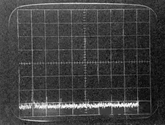
FIG.
11--SPECTRUM ANALYZER PHOTOGRAPH of the 1100-kHz output. (100 kHz/div.
horizontal, 10dB/div. vertical, 500 kHz center frequency, 1t0 kHz resolution
bandwidth)
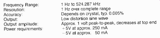
TABLE 1--SPECIFICATIONS
Frequency Range:
Resolution:
Accuracy:
Output:
Output amplitude:
Power requirements:
1 Hz to 524.287 kHz 1 Hz over complete range
Depends on crystal, typ. 0.005%
Low distortion sine wave
Approx. 1 volt peak-to-peak, decreases at top end
+5V at approx. 250 mA
-5V al approx. 50 mA
Construction
A double-sided PC board is available from the source shown in the parts list, and we've also provided the foil patterns in case you want to make your own board. If you're using the PC board, follow the parts-placement diagram shown in Fig. 8.
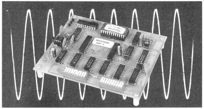
Note that IC5 and 1C8 are high-speed CMOS and must therefore be handled carefully to prevent damaging them. Use a grounded-tip soldering iron (if you've got access to one) and ground your self before picking up the board or an IC. Space for the optional power supply (shown in Fig. 6) is not provided on the PC board, but it can be made on any kind of board. The power-supply circuit is not critical, but be careful due to the line voltages present. Figure 9 shows the completed unit.
Since the majority of the circuit is digital, simple wiring techniques can be used. The author's original prototype was built using wire-wrap methods for the digital section and point to-point for the analog section. If you're wire-wrapping the circuit, some care must be applied to the analog section to prevent digital switching noise from getting into the output. The ground returns for all of the analog section must connect to the power supply separately from the digital section and the analog bypass capacitors must be connected as close as possible to the analog integrated circuits. The oscillator, consisting of IC5-a, R1, R4, C1 and XTAL1, must be tightly wired.
The author's original prototype had the discrete components soldered directly to the wirewrap-socket pins of IC5. A board with an existing ground plane is ideal for wire-wrap construction.
Operation
Before turning on the power, carefully inspect the board for shorts, solder bridges, wiring errors, etc. Set the DIP switch to any non-zero value. If you have a frequency counter available, connect it to pin 5 of IC8-a. If you don't have a counter, adjust C1 to mid-range; with the crystal specified, your error should be no more than about 0.02%. Apply power and, using an insulated adjustment tool, adjust C1 to exactly 2.097152 MHz if you have a counter connected. With an oscilloscope connected to the output, vary the DIP switch setting; you will see the frequency change. For higher and higher frequencies the distortion will increase with the maximum distortion at the highest setting.
The frequency output is equal to the binary value set by the DIP switches, with a logical 1 corresponding to an "off' position. For a switch setting of 001,1000,0110,1010,0000 (100 kHz), the author's prototype gave the waveform shown in Fig. 10. A spectrum-analyzer display of the 100-kHz output is show in Fig. 11. Note that the harmonics are at least 40 dB down, corresponding to about 1% distortion. Varying the least-significant DIP switch will change the frequency output by 1 Hz. Since the frequency is set by the DIP switch and the ac curacy of the crystal oscillator, the output will be the same even after a power-down, power-up cycle. Table 1 summarizes the specifications for the completed digital synthesizer.
Experiments
If the digital parts are changed from 74LS to 74F, the EPROM changed to a bipolar PROM (such as a 74S472 which is accommodated on the circuit board), and the clock oscillator replaced by a faster one, the output frequency can be increased at the expense of resolution. The author has successfully operated the circuit up to a 5.0-MHz output frequency, providing 10 Hz resolution.
The circuit is simple and compact enough that several units can be built to provide fixed calibration frequencies needed on your bench. High-speed CMOS logic may be substituted for the low-power TTL devices for lower-power operation. If you decide to change to CMOS, IC3 must be a 74HCT374 as the output of the EPROM is TTL-compatible. Advanced CMOS, 74AC or 74ACT, should not be used because of noise induced by its fast edge rates.