AMAZON multi-meters discounts AMAZON oscilloscope discounts
OPERATION AND DESIGN
A 250-Volt, 200-MA Vacuum-Tube Voltage-Regulated Supply

Fig. 5-1 . A vacuum tube voltage regulated supply rated at 250 volts, 200
ma.
In Fig. 5-1 we see the schematic diagram of a vacuum-tube voltage-regulated power supply, which is very useful for numerous audio, amateur, and experimental projects. Note that the double-triode input amplifier is a cascaded two-stage DC type rather than a differential amplifier. The added amplification thus obtained produces a low dynamic output impedance, which is considered more desirable for the intended applications than extreme constancy in the output voltage.
Sufficient constancy is brought about by operating VR tube V4 from the voltage which the tube helps stabilize. The price paid for this, however, is that the output voltage cannot be continuously adjusted down to zero volts by adjustment of R13, the 10K potentiometer. If carried too far, the operating voltage across the VR tube will disappear. Also, the two stage voltage amplifier will be deprived of its proper operating voltage before the output voltage can be reduced to zero. The 12K fixed resistance (R12) prevents lowering the output voltage below about 125 volts.
Capacitor C3 (0.25 mfd) in the cathode circuit of the second DC amplifier stage provides AC bypass action in order to prevent AC degeneration due to R7. It is desirable to have high AC amplification in order that the voltage amplifier can effectively filter out the residual ripple in the output. Capacitor C2 modifies the phase characteristic of the amplifier and thereby discourages oscillation. For this connection, capacitances between .01 and 0.1 mfd generally work well. The series losser element (V2 ) is a type 6080 dual triode. The two triode sections are connected in parallel through current equalizing resistors R4 and R5 and operate essentially as a single cathode follower.
In this power supply, the grid of the input amplifier is held at a fixed positive voltage with respect to the negative line. Hence, if AC line or load conditions change in such a direction that the DC output voltage tends to increase, the cathode of the input amplifier will become more positive than the fixed potential at the grid. Such a change in grid-to-cathode bias will decrease the plate current in the input tube.
The later in turn will increase plate conduction in the second DC amplifier (the left half of V3) . The grids of the 6080 control tube (V2 ) will be driven in the negative direction by the increased plate current in the second amplifier stage.
The final result is lower conduction in the control tube--which is tantamount to saying that the change in DC resistance of the 6080 tube nearly restores the DC output voltage to its previous value. The converse sequence of events occurs if the output voltage tends to drop. In this way, the output voltage is stabilized at a discrete value controlled by the adjustment of the 10K potentiometer.
Transistorized Shunt-Voltage Regulator
Fig. 5-2 is an example of a closed-loop voltage regulator with the variable losser connected across the load rather than in series with it. If the output voltage tends to increase, the losser element (transistor X5) will receive an error signal which increases the conduction through its emitter-to-collector circuit. This increases the voltage drop across R11l, thereby depriving the load of the voltage change responsible for the error signal. The converse conditions apply when the output voltage tends to decrease. In this way, the voltage across the load is maintained at a fixed value. Although a closed loop is involved, the ultimate action is similar to that in a simple VR-tube or zener-diode circuit. Note that the effective resistance of the shunt element must change in the opposite direction from that of a series-connected losser in order to accomplish like results.
An interesting feature of the circuit in Fig. 5-2 is that voltage reference M1, differential-amplifier stage X1-X2, and voltage-amplifier stage X3 all have individually regulated power sources, which contribute toward stability and also enable control of the regulated voltage output down almost to zero volts. This design is well suited for developmental work with transistor circuitry. Short-circuited output terminals do not damage or overload any elements. The parts data for this circuit are provided in Table 5-1 .

Fig. 5-2

Table 5-1. Transistor and semiconductor diode data for circuit of Fig. 5-2.

Fig. 5-3. A high-voltage regulated power supply for traveling-wave tubes.
A High-Voltage Regulated Supply
The voltage-regulated supply shown in Fig. 5-3 is capable of providing up to several milliamperes to the collector of a traveling-wave tube, with voltage regulation on the order of 0.1 % (line or load) . Output voltage is adjustable from 1,600 to 2,100 volts. Additionally, VR tubes provide a selection of less precisely regulated voltages for the anode of the traveling-wave tube. Tubes V8, V9, V6, and V7 constitute the voltage reference, comparator and DC amplifier, and series losser for regulation of the high voltage provided by rectifiers V10 and V11.
The circuit as described thus far would be operative and would be typical of many vacuum-tube voltage regulators.
However, in order to obtain closer regulation and higher stability, the voltage applied to the VR tubes is also regulated.
This function is provided by tubes V2, V3, and V4, which stabilize the voltage delivered by full-wave rectifier V1. It is interesting to note that VR tubes V8 and V9 belong as much to the regulator circuit associated with V2, V3, and V 4 as to the regulator circuit associated with V5, V6, and V7.
V 4, a dual triode connected as a differential amplifier, is the comparator and first DC amplifier stage of the voltage regulator for the VR tubes. V3 is the second stage and has a similar circuit configuration. V2 is the controllable series losser.
Table 5-2 gives the tube types and their circuit functions for the power supply in Fig. 5-3.
A 2.5-Ampere Voltage-Regulated Power Supply
Despite the extremely simple circuit configuration of the voltage-regulated power supply shown in Fig. 5-4; the performance is more than adequate for the requirements of many high-current loads. It would be both impractical and Table 5-2. Vacuum-tube data for the circuit in Fig. 5-3 difficult to obtain high current and low voltage from tube circuits ; yet this type of output is a natural for transistors.
An unusual aspect of this supply is that there is no voltage amplification of the error signal. Transistors X1 and X2 are both emitter followers and provide current amplification only. In essence, they improve the impedance match between reference diode M5 and the base of series losser X3. This enables X3 to develop optimum power sensitivity as a variable series control element in this circuit. Consequently, the regulation characteristics are much better than they would be without X1 and X2. Although voltage amplification is generally provided in the error-signal amplifier of regulator circuits, it is always the over-all power amplification which enables closer regulation to be achieved. In tube-regulator circuits, the power amplification is usually obtained by voltage gain alone, because the losser tube seldom operates deeply in its positive-grid (current-consuming) region. With transistor losser elements, input current is consumed ; and even when the error signal is amplified considerably, at least one emitter-follower stage is required in order to satisfy the current demand of the losser transistor.

Fig. 5-4. A series regulator with a continuously variable output voltage
from 0 to 10 volts and a current rating of 2.5 amperes.
This voltage-regulated power supply is well suited for energizing the DC control winding of magnetic amplifiers.
As a source of filament power, it will prove beneficial in minimizing hum problems in audio equipment and delicate instrumentation techniques. Table 5-3 gives the transistor and diode types used in this circuit, and their function.

Table 5-3. Transistor and semiconductor diode data for the circuit of Fig.
5-4

Fig. 5-5. A solid-state voltage-regulated supply that will deliver 150 volts
at 500 ma.
A 150-Volt, 0.5-Ampere Solid-State Voltage-Regulated Power Supply
The fully transistorized voltage regulator shown in Fig. 5-5 is unique in that the voltage output is considerably higher than the several tens of volts often obtained from solid-state regulators. Differential amplifier X5-X4 is powered from the regulated output. X3 is a voltage-amplifier stage whose operation is stabilized by zener diode M3 connected to its emitter circuit, and also by zener diode M4 in its collector circuit.
M4 additionally prevents introduction of hum into the base of X2 through the 1K biasing resistor. X2 is an emitter follower stage which provides a reasonable impedance match between the collector of voltage amplifier X3 and the base of series losser element X1. The presence of X2 enables X3 to develop a much higher voltage gain than would otherwise be the case.

Table 5-4. Transistor and semiconductor diode data for the circuit of Fig.
5-5
Although 150 volts appears at the output terminals, the emitter-to-collector voltage of series losser X1 is in the neighborhood of one-tenth this value. In the event of a short circuit at the load, the full output voltage from the rectifier will then be impressed across X1 and destroy it. Hence, extreme precaution must be taken to prevent such an occurrence. Obviously, this supply is not suited for experimental work. Other transistor-regulated supplies, which operate at lower voltages and generally at higher currents, can survive momentary short circuits due to the thermal lag of the larger transistors used in the series control function. With such supplies, a fuse or a fast circuit breaker can provide additional protection. This power supply could be made short-circuit proof by additional electronic circuitry, which would instantaneously shunt the emitter of X1 to its collector. Providing cutoff bias to the base of X1 (a popular short circuit protection in lower-voltage supplies ) would not be suitable here because X1 must be protected from excessive voltage as well as excessive current. (Refer to Table 5-4 for transistor and semiconductor diode data for this circuit.)

Fig. 5-6. A transistorized series regulator with output adjustable from
0 to 2S volts at 2 amperes.
Transistor Voltage-Regulated Supply with Overcurrent Protection
The voltage-regulated supply shown in Fig. 5-6 is typical of many transistor regulator circuits, but it also involves circuitry which greatly enhances its practicability. Note that the AC windings of the magnetic amplifier are inserted in series with one AC line of the power-transformer secondary.
The control winding of this magnetic amplifier receives DC current through transistor X1 from a separate 12-volt DC power supply. The base of X1 is impressed with conduction bias from the voltage appearing at the output terminals of the regulated supply. As a result, X1 is normally biased for high emitter-to-collector conduction, thus permitting a heavy current to flow into the control winding of the magnetic amplifier. The core of the magnetic amplifier is magnetically saturated, and the AC windings have very little inductance. Therefore, nearly all the AC voltage developed in the secondary of the power transformer is impressed across the main rectifier bridge, and normal power-supply operation occurs.
In the event of a short circuit at the output terminals, X1 will be deprived of its forward-conduction bias. The control winding of the magnetic amplifier will then receive little or no DC magnetization current. This, in turn, results in a high inductance in the AC winding, because the flux in the core is now considerably below the densities corresponding to magnetic saturation . The high inductance limits the voltage output of the power supply, thereby protecting X2 and X3 from excessive power dissipation. Inasmuch as X2 and X3 are large power transistors and are heat-sinked to aluminum or copper plates, the response lag inherent in magnetic amplifiers is of little practical consequence, and reliable protection is obtained . Another feature of this regulator is the circuit provision for continuous adjustment of the regulated output voltage from 0 to 25 volts. This is done by the more or less conventional method of using a variable resistance at the input circuit of the differential amplifier. However, it is ordinarily difficult to reduce the output voltage beyond a nominal amount because the series losser transistor (s) then must operate with a relatively high collector-to-emitter voltage.
It is evident that the losser transistor must absorb the difference between the voltage from the rectifier system and the voltage across the load. If the load voltage is lowered too much, the losser transistor will be subjected to a relatively high voltage. Although this transistor may have an adequate voltage rating, it will also have to dissipate inordinately high power when the load consumes the rated current. It becomes impractical and uneconomical to use a losser transistor having the power-handling ability to withstand such service. This problem can be circumvented by inserting a variable autotransformer in the primary circuit of the main power transformer and mechanically ganging it to the voltage control resistance (potentiometer ). As a result, the voltage output of the main rectifier system will automatically of Fig. 5-6.

Table 5-5. Transistor and semiconductor diode data for the circuit be reduced
as the load voltage is lowered. Therefore, the voltage drop across losser
transistors X2 and X3 will be maintained at a low, almost constant value.
In order that the load voltage may be adjusted down to zero, separate regulated power supplies are provided for amplifiers X8, X7, X6, and X5. Transistor X4, the driver for X2 and X3, operates from the unregulated supply line and is thereby ensured an operating voltage for any adjustment of the regulated output voltage. Table 5-5 gives the type number and function of the transistors and zener diodes used in Fig, 5-6.
A 1.5-Ampere Current-Regulated Power Supply
In the current-regulated power supply, the input amplifier compares a reference voltage with a sampled voltage. The latter is proportionate to the current delivered by the supply, rather than to the voltage across the output terminals (as in voltage-regulated supplies ). Thus, in Fig. 5-7 the 10?ohm series resistance provides a voltage drop that is directly proportionate to the current flowing through it. Should the load current increase, X3 will be deprived of sufficient forward bias to lower the load current to its nominal regulated value. The converse action occurs if the load current should tend to decrease. An error signal of appropriate sign and amplitude appears at the base of X1 to restore the output current to its nominal regulated value whenever the line voltage or load resistance changes. The error signal then Table 5-6. Transistor and semiconductor diode data for the circuit of Fig. 5-7
restores the load current to its regulated value. This value may, however, be adjusted over a wide range by means of the 75-ohm potentiometer.
Fig. 5-7. A 1.5-ampere current-regulated power supply.
Fig. 5·8. Basic output terminal arrangement for remote sensing.
The 50-ohm resistance connected across losser transistor X3 protects the latter from the voltage surges produced when inductive loads are switched (not recommended ). This resistance is not low enough to seriously impair the current regulation. A large capacitor in this circuit position is also helpful here. X2, which is commonly an emitter follower in voltage-regulated supplies, is connected in the common-emitter configuration. Although little voltage amplification is obtained from this stage, it does provide the necessary phase inversion so that the effective resistance of X3 will change in the proper direction and thereby regulate the load current. Table 5-6 gives the transistor and semiconductor diode data for Fig. 5-7.
REMOTE SENSING OF THE LOAD
No matter how closely a supply is voltage regulated , the wiring between the output terminals and load will always tend to increase the output resistance and dynamic impedance. This can be avoided by freeing the ends of the voltage sampling network from their connections to the positive and negative output terminals. Separate connections are then made between the voltage-sampling network and load terminals. A typical power supply making use of such a provision is illustrated in Fig. 5-8. The positive and negative output terminals (A and D, respectively) are connected to the load-which, for the purpose at hand, is assumed to be some distance from the power supply. As a consequence, an appreciable potential drop occurs in wires AE and DF. If terminal A were connected to terminal B, and C to D (as indicated by the dashed lines in Fig. 5-8) , the voltage regulation across load terminals EF would not be as good (that is, as low) as the regulation across terminals AD. On the other hand, suppose terminals B and C are connected by extra wires to load terminals E and F (rather than to A and D) . Then the resistance of wires AE and DF will be regulated out.
Wires BE and CF can be of relatively small gauge, since they do not carry appreciable current. Wires AE and DF must have large enough cross sections to comply with safety requirements. However, they need not be selected primarily to maintain regulation, because their resistances will now be effectively reduced by the gain of the amplifiers in the power supply. Thus, although four wires are required instead of two, less copper is needed to interconnect the power supply and remote load.
POSITIVE REGULATION

Fig. 5-9. A 180-volt, 150-milliampere voltage regulator that has provision
for positive regulation.

Fig. 5-10.
It is possible to make the load voltage actually rise in response to a decrease in AC line voltage or an increase in load current. Although such overregulation is not frequently desired, the techniques for accomplishing it are sometimes useful as a means of more closely approaching zero regulation. For example, in Fig. 5-9 the screen grid of DC voltage amplifier V2 can be, to an adjustable degree, supplied from the unregulated DC side of series losser tube V1. The screen grid of the pentode acts as another control grid in the electron stream. Much lower voltage amplification is displayed at the plate, with respect to small variations of screen-grid voltage, than to like variations at the control grid. However, the excursions of unregulated DC voltage (resulting from changes in the AC line voltage) can be considerably greater than the variations in amplitude of the error signal at the control grid. Therefore, permitting the screen grid to sample the unregulated DC voltage can exert considerable effect on the regulating characteristics of the circuit.
In this circuit, R1 (the 50K potentiometer) is adjusted to provide the desired amount of overcompensation. The 100,000-ohm potentiometer (R2) permits compensating for the effect which the adjustment of R1 has on the screen-grid voltage ; the intended function of the latter potentiometer is not to change the screen-grid voltage, but rather its source.
These adjustments can be facilitated by connecting a voltmeter between the screen grid and cathode of V2. If R2 is then adjusted to maintain a constant screen-grid voltage as R1 is also being adjusted, the regulating characteristics of the circuit can be varied while the nominal output voltage is held at nearly a fixed value. Adjustment of the nominal output voltage is conventional, being provided by 250K potentiometer R3 in the control-grid circuit of V2.
Another method of providing overregulation is shown in the solid-state voltage regulator of Fig. 5-10. Differential amplifier X5 senses the load current as well as load voltage.
The voltage drop developed across R1 (the 5-ohm potentiometer) or a portion of it constitutes the emitter-to-base bias for X5. This bias, through the amplifier chain, causes X1 to raise the DC output voltage as the load current increases. Thus, this circuit has positive current feedback, in addition to the conventional negative voltage feedback. This type of overregulation frequently occurs inadvertently in heavy-current supplies. In such instances, the current-sensing resistance exists in the connecting wire itself.
A VOLTAGE REGULATOR USING COMPLEMENTARY SYMMETRY
An interesting voltage regulated power supply is shown in Fig. 5-1 1. By means of complementary symmetry, an Table 5-7. Transistor and semiconductor diode data for the circuit of Fig. 5-11
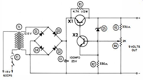
Fig. 5-11. Representative complementary symmetry voltage regulator power
supply.
NPN transistor functions as a comparator IDC amplifier and a PNP transistor operates as a series losser. Note that the output is derived from the collector of the PNP transistor, rather than the emitter as is generally encountered in regulator circuits employing like-poled transistors through
out. The series losser transistor performs as an emitter follower stage. This can be readily seen by considering that the basic relationships pertaining to an emitter follower stage are not altered by interchanging the DC supply to the collector and the load. A unique feature of this circuit is that the performance is, for many applications, not down-graded by the use of a relatively inexpensive germanium PNP transistor and silicon NPN transistor. The circuit is very flexible, however, and will perform well with various combinations of different PNP and NPN transistors. This includes the use of an NPN series losser and a PNP voltage amplifier, if considerations other than the cited cost factor so dictate. (Of course, such an inversion requires appropriate changes in the polarities of the applied direct current and the zener diode.) Fig. 5-11 together with table 5-7 specify components suit
able for operation at 9 volts. This makes the power supply useful as a substitute DC source for the home operation of small transistor radios. When so used, a surprising improvement in quality of sound reproduction will generally be observed. This is because the so-called "transistor radio sound" is overcome. The distortion is not due primarily to the small speaker as is commonly supposed, but is a consequence of the poor dynamic regulation of transistor batteries. Most of these sets employ push-pull class B output stages. A poorly regulated power source is one of the most conducive factors for generating distortion in class B amplification. This seems to be even more the case with transistors than with tubes wherein the closer match permits better cancellation of even order distortion products.
This regulated supply can also be used to operate the transistor radio from the 12-volt automobile battery. Many of these sets are sufficiently sensitive and operate quite well from their own ferrite antenna.

Fig. 5-12. Simplified schematic of a high-voltage regulator circuit in
a color tele· vision circuit.
Fig. 5-12 is a simplified circuit of a shunt-voltage regulating technique found in a number of color television receivers. In this circuit the 6BK4 shunt regulator tube works in conjunction with the internal resistance of the 3A3 half wave rectifier. The objective is to maintain the nominal 25 kilovolts applied to the cathode ray tube at a near-constant value so that picture size, brightness and hue will not vary with AC line voltage and the setting of the various panel adjustments. There is no voltage reference used, but the regulating action is quite suitable for the intended purpose.
The error signal is derived from the B+ boost voltage. Boost voltage is obtained from the damper circuit (not shown ) and is a dependent function of the high voltage developed in the flyback transformer. A rise in the rectified output voltage, for any reason, produces a higher boost voltage.
A portion of the higher boost voltage appears at the control grid of the shunt regulator making it more conductive. The high-voltage supply is accordingly loaded more heavily and its output voltage drops.