AMAZON multi-meters discounts AMAZON oscilloscope discounts
Semiconductor devices are used for amplification, oscillation, modulation, demodulation, and other applications such as waveshaping. Fig. 1-1 shows the physical construction of pnp and npn junction transistors. Fig. 1-2 shows the general types of waveforms associated with amplification, oscillation, amplitude modulation, amplitude demodulation, frequency modulation, and frequency demodulation. A transistor may be used in a current, voltage, or power amplifier configuration. A signal of 1 mA fed into the input of a transistor may appear at a 20-mA level in the output circuit.
As an oscillator, a transistor converts DC voltage into ac volt age. In suitable circuit arrangements, a transistor can provide amplitude modulation (variation in amplitude of an rf signal), or frequency modulation (variation in frequency of an rf signal). Demodulation of a-m and fm signals can be accomplished by transistors in associated circuit configurations. A transistor may also be used to shape one waveform into another wave form. Fig. 1-3 illustrates the application of a transistor as a waveshaper to change a sine wave into a square wave. The operation of a transistor as a clipper is also shown. Basically, a transistor is an electronic valve that permits collector supply current in step with an input waveform. With a suitably chosen bias, collector current will be permitted only over a certain portion of the input signal cycle.
A transistor has two junctions, which can be operated as rectifiers. Whether a transistor amplifies, modulates, demodulates, or clips, depends on the emitter-junction bias. Fig. 1-4 shows the voltage-current characteristic of a pn junction.
Diodes cannot amplify, unless they are of the tunnel-diode construction. This function of a diode is discussed subsequently.
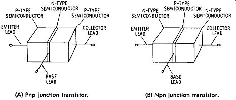

Fig. 1-1. Transistor construction. (A) Pnp junction transistor. (B) Npn junction
transistor.
(A) Amplifier. (B) Oscillator. (C) Amplitude modulator. (D) Amplitude demodulator. (E) Frequency modulator. (F) Frequency demodulator.

Fig. 1-2. Transistor applications.
However, any diode operates as a modulator or demodulator if it is biased to a nonlinear interval of its voltage-current characteristic. The advantage of a transistor in modulation and demodulation action is the amplification, and consequently the stronger output signal, that is provided by the collector circuit. Diodes cannot oscillate, unless they are of the tunnel diode construction. Both diodes and transistors can give squaring and clipping action, although a transistor provides a stronger output signal.

Fig. 1-3. Transistor used to modify waveforms. (A) Squaring action. (B) Clipping
action.

Fig. 1-4. Current-voltage curve for pn junction.
BASIC WAVEFORM ANALYSIS
There are certain principles of waveform analysis that we should understand at this point. Signal processing, in theory, could be described with reference to any fundamental waveform that we might choose. For example, we could choose a square wave as our fundamental waveform; however, this would be a poor choice, because it becomes very complicated to build up a sine wave, or pulse, or sawtooth wave, from a mix ture of square waves. In practice we find only two waveforms that are suitable for use as fundamental waveforms. These are the sine wave and the exponential wave. The utility of these two fundamental waveforms stems from mathematical principles that we can neglect at this point. Instead, we will simply state that all waveforms can be regarded as built up from combinations of sine waves and/or exponential waves.
Let us consider the build-up of a square wave from sine waves, as shown in Fig. 1-5. In theory, an infinite number of harmonics would have to be combined with the fundamental sine wave to produce a perfect square wave. In practice, how ever, we find that about 20 harmonics suffice to give a reason able facsimile of a square wave. This idea of square-wave com position is very useful because it can be used to explain how a square wave is modified when it passes through various kinds of circuits. For example, if a good square wave is applied to an amplifier that has limited bandwidth, we perceive that the higher-frequency harmonics cannot get through to the output of the amplifier. In turn, the rise time of the square wave is slowed down, in accordance with the highest harmonic that is passed by the amplifier.

Fig. 1-5, Synthesis of square wave from sine waves.

Fig. 1-6. Rise time (T ,) of square wave.
This is such an important and basic consideration that it is advisable to explain some of the details that are involved. It is evident that wave Crises faster than wave A in Fig. 1-5. Similarly, wave E rises faster than wave C, and wave G rises faster than wave E. In practice, we need to know how the rise time of an output square wave is related to the high-frequency cut off point of an amplifier. This is a simple formula that is written: where,
1 Tr= 3f,_ Tr is the rise time of the output square wave, (1.1)
fc is the frequency at which the amplifier response is down 3dB.

Fig. 1-7. High-frequency cutoff point f, ..
Fig. 1-6 illustrates the meaning of rise time. Rise time is measured between the 10-percent and 90-percent points on the leading edge of a square wave. Accurate measurement requires the use of a scope with calibrated and triggered sweeps. The waveform is greatly expanded on the triggered-sweep function so that its leading edge occupies a substantial portion of the horizontal interval. In turn, the 10-percent and 90-percent points are noted, and the rise time is read from the settings of the calibrated sweeps. The -3-dB point of an amplifier response curve occurs at the point where the output voltage falls to 0.707 of its maximum value. This is shown in Fig. 1-7. Since the out-put power is reduced one half at the -3-dB point, the high frequency cutoff point is also called the half-power point.
In spite of the utility of Fig. 1-5 in giving a general description of what causes reduced rise time, we must be on our guard to avoid absurd conclusions. In other words, the relations in Fig. 1-5 are not completely descriptive of amplifier action. For example, we might suppose from inspection of Fig. 1-5 that if a square wave is passed through an amplifier that has a narrow bandwidth, and that all harmonics above the 7th harmonic are removed, the reproduced waveform would have a "wavy" top.
However, this is not so--the waveform will have a flat top.
This example of square-wave analysis has given us an unexpected test result. Let us analyze the situation to see why our conclusion was incorrect.

Table 1-1. DB expressed ;as power and voltage (or current) ratios.

Fig. 1-8. Bandwidth concepts. (A) In radio-receiver circuit. (B) In TV-receiver
circuit.
When a square wave is applied to an amplifier, we do not actually apply a combination of sine waves. That is, we have merely stated thus far that a square wave could be built up or synthesized from a large number of sine waves. The fact of the matter is that a square wave is generated by switching a DC voltage on and off. There is more than one way of looking at a switched DC voltage. We can state that the waveform could be built up from a large number of sine waves. This is quite a different situation from what the generator actually does--it merely switches a DC voltage on and off. Therefore, we must ask what the amplifier response will be to a DC voltage that is suddenly applied and then as suddenly removed. This gets us into the relation between square waves and exponential wave forms; details must be reserved for subsequent discussion.
Fig. 1-7 shows the relation between a voltage value and a dB value. A tabulation of these relations is given in Table 1-1.
Amplifier bandwidth is measured in two different ways. In the case of a radio receiver, the bandwidth is defined as the number of hertz between the -3-dB points on the frequency-response curve. On the other hand, in the case of a TV receiver, the bandwidth is defined as the number of hertz between the -6-dB or 50 percent-of-maximum voltage points. Examples are shown in Fig. 1-8. In many cases, lab-type scopes have graticules with dB scales. To locate a -3-dB or a -6-dB point on a response curve, we adjust the waveform as depicted in Fig. 1-9. Then, dB points can be read directly from the scope screen.

Fig. 1-9. Scope graticule calibrated in dB values.
Next, let us review the basic voltage of a sine wave, as shown in Fig. 1-10. Service-type VOM's read the rms value of a sine wave. Therms value is equal to 0.707 of the peak voltage (either positive or negative peak). In turn, the peak-to-peak voltage of a sine wave is equal to twice the peak voltage. It follows that the peak voltage is equal to 1.414 times the rms voltage, and that the rms voltage is equal to the peak voltage divided by 1.414.
Again, the rms voltage of a sine wave is equal to its peak-to peak voltage divided by 2.83. These are important voltage relations that are not always clearly understood by beginners.

Fig. 1-10. Fundamental sine wave. (A) Sine waveforms with same amplitude.
(B) Sine waveforms with same frequency. Courtesy Allied Radio Corp.

Fig. 1-11. Distinction between amplitude and frequency.
It is evident that the voltage of a sine wave is not related to its frequency. They are independent parameters. This fact is illustrated in Fig. 1-11. It must be emphasized that the relations among rms, peak, and peak-to-peak values that have been cited for a sine wave are not true for other waveforms, such as square waves. Therefore, it is customary to compare various waveform amplitudes only in terms of their peak-to-peak values. The peak-to-peak voltage is of chief concern in analysis of transistor circuit action, and we seldom investigate the rms voltage of a complex waveform. It follows that when we calibrate a scope with a VOM, we must use a sine-wave source, multiply the VOM reading by 2.83 to obtain its peak-to-peak value, and then calibrate the scope in terms of this peak-to peak voltage. For example, if we start with a 6.3-volt sine-wave source, its peak-to-peak voltage is equal to nearly 18 volts.
Therefore, the vertical deflection on the scope screen represents approximately 18 volts pk-pk.
After a scope has been calibrated in peak-to-peak voltage values, the peak-to-peak voltage of any complex waveform can be read directly from the screen. Fig. 1-12 illustrates this principle. Note that peak-to-peak values are equivalent to dc values; that is, we can calibrate a DC scope from a DC voltage source, and employ this calibration for measurement of peak to-peak voltages. The sine wave depicted in Fig. 1-10 has a positive half-cycle and a negative half-cycle; similarly, the square wave has a positive half-cycle and a negative half-cycle.
On the other hand, the "+ pulse" has a positive excursion only.
Similarly, the "- pulse" has a negative excursion only. These terms are related to the DC component of a pulse, as explained subsequently. The complex wave has a positive half-cycle and a negative half-cycle.

Fig. 1-12. Different waveforms having same peak-to-peak voltage.

Fig. 1-13. Three basic combinations of ac and DC values.
In summary, an ac waveform (a waveform with both positive and negative excursions) has no polarity indication. For example, the sine wave, square wave, and complex wave depicted in Fig. 1-12 have no polarity indications. On the other hand, a DC waveform has a polarity indication; thus, the two pulse waveforms in Fig. 1-12 are marked positive and negative, respectively. These are called DC pulses because their total excursion is a single polarity. We will find that an ac pulse can be changed into a DC pulse, or vice versa, by suitable variation of the DC component. Accordingly, let us observe the distinction between an ac voltage, a pulsating DC voltage, and an ac volt age with a DC component, as depicted in Fig. 1-13.
An ac waveform has an average value of zero. This simply means that the area of the positive half-cycle is equal to the area of the negative half-cycle. In other words, if we apply an ac waveform to a DC voltmeter, the pointer does not deflect.
However, a pulsating DC waveform has a DC component; this DC component exceeds the peak value of the ac component, and therefore, the waveform does not cross the 0-volt axis. In the example shown in Fig. 1-13, the pulsating DC waveform has a positive excursion only. The average value of a pulsating DC waveform is not zero; if we apply a pulsating DC waveform to a DC voltmeter, the pointer indicates the value of the DC component in the waveform. Finally, an ac waveform with a DC component crosses the 0-volt axis, because the DC component has a value that is less than the peak value of the ac component. An ac waveform with a DC component has both positive and negative excursions. Its average value is not zero; if we apply an ac waveform with a DC component to a DC voltmeter, the pointer indicates the value of the DC component in the waveform.
With this understanding of the distinctions among ac wave forms, pulsating DC waveforms, and ac waveforms with DC components, let us consider the positive square wave depicted in Fig. 1-14. The bottom of the square wave touches the 0-volt axis, but does not cross the axis. Therefore, this is a pulsating DC waveform. We note that this positive square wave is formed by combining an ac square wave with a DC component that has a value equal to the peak voltage of the ac square wave. Note that when an ac square wave is changed into a DC square wave, the peak voltage of the waveform is doubled. That is, peak voltage is measured from the 0-volt axis. If we add a positive DC voltage to an ac waveform, the positive-peak voltage of the ac waveform is increased by the value of the DC component. Of course, this process decreases the negative peak voltage of the ac waveform by an amount equal to the value of the DC component.

Fig. 1-14. Square wave with positive excursion only.
WAVEFORMS IN TRANSISTOR AMPLIFIER CIRCUITS
Most waveforms processed by transistor amplifiers are pulsating DC waveforms, as shown in Fig. 1-15. The reason for this occurrence is that DC bias voltages are applied to the base and collector of the transistor. Moreover, a transistor cuts off if it is reverse-biased. With reference to Fig. 1-15A, a negative DC bias is applied to the base of the transistor, and a negative DC voltage is applied to the collector. An ac signal voltage is coupled into the base of the transistor; here, the ac waveform combines with the DC bias voltage to produce a pulsating DC waveform. As seen in the inset, this waveform has a negative excursion only.
Next, in Fig. 1-15A, the pulsating DC signal that flows into the base diffuses into the collector circuit. Since the collector operates at a higher DC voltage than the base, the drop across RL is much greater than the drop between base and emitter.
In other words, voltage amplification is obtained in the collector circuit. Of course, the collector output waveform is also a pulsating DC waveform; the output waveform has a negative excursion only. Note that the ac component of the output wave form is reversed in phase, compared with the ac component of the input waveform.

Fig. 1-15. Pulsating DC waveforms in transistor amplifier circuits. (A) Pnp
grounded emitter. (B) Npn grounded emitter.
Next, if we use an npn transistor, as shown in Fig. 1-15B, the polarity of the pulsating DC waveforms is reversed. That is, the base of the transistor is biased positively, and a positive voltage is applied to the collector. An ac signal is coupled into the base of the transistor; here, the ac signal combines with the positive bias voltage to form a pulsating DC voltage. This waveform has a positive excursion only. The pulsating DC waveform diffuses through the base into the collector circuit, where it appears as an amplified pulsating DC waveform. Its ac component is reversed in phase, but the output waveform nevertheless has a positive excursion only.
It is important for us to note that a coupling capacitor re moves the DC component of a pulsating DC waveform, as shown in Fig. 1-16. We observe that the input waveform has both an ac component and a DC component. However, the capacitor blocks the DC component; therefore, only the ac component appears on the output end of the capacitor. A transformer has the same action on a pulsating DC waveform; the transformer blocks the flow of de, and when a pulsating DC waveform is applied to the primary, only the ac component appears at the secondary.

Fig. 1-16. Capacitor does not pass DC component.
Pulsating DC waveforms in the CB (common base) and CC ( common collector) transistor amplifier circuits are seen in Fig.1-17. Observe in Fig. 1-17A that the CB configuration does not reverse the signal phase from input to output. However, the emitter of the pnp transistor is biased positively, and a negative DC voltage is applied to the collector. In turn, the input waveform has negative polarity, but the output has positive polarity. Both are pulsating DC waveforms, but their polarities are reversed from input to output. If an npn transistor is used, as shown in Fig. l-17B, the input waveform has positive polarity, but the output waveform has negative polarity. Both are pulsating DC waveforms.
In the CC transistor amplifier configuration shown in Fig. 1-17C, the output waveform has the same phase as the input waveform. The base is biased negatively, and the emitter is biased positively with respect to the base. Note carefully that current flow through the emitter load resistor produces a volt age drop that is negative with respect to ground. Therefore, the output waveform has negative polarity. In this arrangement, the input waveform is a negative pulsating DC voltage, and the output waveform is also a negative pulsating DC volt age. Next, with reference to Fig. 1-17D, the polarities are re versed because an npn transistor is used in the circuit. The input waveform is a positive pulsating DC voltage, and the out put waveform is also a positive pulsating DC voltage.
If we use a DC scope to check the waveforms at the input and output terminals of a transistor amplifier, we observe a pat tern such as illustrated in Fig. 1-18. Note that when no signal is applied to the vertical-input terminals of the scope, the beam rests at the 0-volt level. Next, when a pulsating DC signal is applied to the scope, the ac component of the waveform is displaced above the 0-volt level (assuming that the DC component is positive). The average value of the ac waveform rests at the DC component level in the pattern. If the scope has been calibrated, we can read the DC component voltage and the ac component pk-pk voltage directly from the screen.
The beginner should carefully note that the pattern shown in Fig. 1-18 is obtained only if a DC scope is utilized. If we employ an ac scope, the sine wave will not be displaced above the 0-volt level. Instead, the sine wave will appear centered on the 0-volt level. This is just another way of saying that an ac scope removes the DC component from a pulsating DC wave form. In turn, the DC component level coincides with the 0-volt level when an ac scope is used. Therefore, an ac scope cannot be used to measure the value of the DC component in a pulsating DC waveform.
(A) Common-base pnp transistor.
(C) Common-collector pnp transistor.
(B) Common-base npn transistor.
(D) Common-collector npn transistor.

Fig 1-17. Waveforms in common-base end common-collector configurations.

Fig. 1-18. Response of DC scope to ac voltage having DC component.
PULSE VOLTAGES
Some of the circuits in transistor TV receivers process pulse waveforms. Therefore, it is important for us to clearly under stand the voltages that are specified in a pulse waveform. Fig. 1-19 shows the voltages in an ac pulse waveform. The positive peak voltage is not equal to the negative-peak voltage. To find the peak-to-peak voltage of the pulse, we add the positive-peak and the negative-peak voltages. If this waveform is displayed on the screen of either a DC or an ac scope, the 0-volt axis of the pulse waveform coincides with the 0-volt level on the scope screen. In turn, if the scope is calibrated, we can read the values of the positive-peak voltage and of the negative-peak volt age directly from the screen.
Note carefully that the average of the ac pulse pictured in Fig. 1-19 is zero. This means that if the ac pulse is applied to a DC voltmeter, the pointer will not deflect. An average value of zero stems from the fact that the area enclosed by the positive excursion of the pulse waveform is exactly the same as the area enclosed by the negative excursion. Coulomb's law for quantity of electricity, or charge flow, is formulated: Et Q=It=1r where, Q is charge in coulombs, t is time in seconds, I is current in amperes, E is potential in volts, R is resistance in ohms.
(1.2)
Since the load resistance has a fixed value in a transistor amplifier circuit, the current value is proportional to the volt age value. Therefore, we recognize that voltage in Fig. 1-19 is proportional to current. In turn, the area enclosed by the positive excursion of the pulse waveform is proportional to the product of current and time. Similarly, the area enclosed by the negative excursion of the pulse waveform is proportional to the product of current and time. Formula (1.2) states that the product of current and time is equal to the quantity of electricity, or value of charge flow. In an ac pulse waveform, the positive and negative areas are always exactly equal. Consequently, there is just as much positive electricity in a pulse waveform as there is negative electricity, and the average value of the ac pulse waveform is necessarily zero.

Fig. 1-19. Voltages in ac pulse waveform (positive and negative areas equal).

Fig. 1-20. Average value of DC pulse is equal to its DC component value.

Fig. 1-21. Graphical definition of rise time.
Next, let us change the ac pulse shown in Fig. 1-19 into a DC pulse. This can be done by combining the ac pulse with a positive DC voltage that has a value equal to the negative peak voltage of the pulse waveform, thus obtaining a positive pulsating DC waveform. This waveform will have a positive peak voltage equal to the peak-to-peak voltage of the ac pulse. With reference to Fig. 1-20, it can be seen that the average value of a positive pulse is equal to its DC component value. That is, if we put the unshaded area A into the space indicated by the shaded area A, we have converted the DC pulse into a steady DC voltage. This means that if a DC pulse is applied to a DC volt meter, the voltmeter will read the value of the DC component in the pulse.
Fig. 1-21 shows the meaning of the rise time of a pulse. Of course, a pulse has the same rise time, whether it is checked on a DC scope or an ac scope. In other words, the presence of a DC component in a pulse does not affect its rise time. If the pulse happens to have a DC component, the only difference be tween an ac scope display and a DC scope display is that the DC component will shift the waveform vertically on the screen of a DC scope. This results from the fact that application of a DC voltage to a DC scope shifts the trace vertically, as shown in Fig. 1-22.
(B) Zero volts applied. (C) Positive volts applied. (D) Negative volts applied. Courtesy Allied Radio Corp.

Fig. 1-22 Application of DC voltages to d scope.

Fig. 1-23. Block diagram of typical synchroscope
RISE-TIME MEASUREMENT
Measurement of the rise time of an output pulse or square wave is a basic procedure in the analysis of various transistor amplifiers and various other transistor configurations. There fore, we must know how to measure rise time. This is accomplished best by use of a triggered-sweep scope with calibrated time bases. A scope of this type used in pulse work is called a synchroscope. Fig. 1-23 is a block diagram for a typical synchroscope. Its central feature is a start-stop sweep generator; that is, the forward deflection interval does not start until the leading edge of a pulse (or other waveform) arrives via the sync amplifier. This feature facilitates the measurement of elapsed time.
(A) Input pulse. (B)Without delay. (C) With delay.

Fig. 1-24. Effect of delay on synchroscope trace.
Another important feature of the synchroscope depicted in Fig. 1-23 is the provision of a delay line in the vertical-amplifier channel. In this example, the delay line holds the incoming waveform for 1/2 microsecond before it is passed through to the vertical-deflecting plates. This provision is necessary in order that the entire leading edge of the waveform may be displayed on the scope screen-it takes almost 1/2 microsecond for the start-stop sweep circuit to "get started." Fig. 1-24 shows the effect of the delay line on an applied pulse. The input pulse is depicted at A; if no delay line is employed, the sweep circuit is slow in getting started, with the result that part of the leading edge is missing in the displayed waveform, as shown at B. However, when a delay line is used, the pulse waveform is held back for 1/2 microsecond in the vertical channel, and the sweep circuit is given ample time to start.
In turn, the complete leading edge of the pulse is displayed on the scope screen, as seen at C.
ACTION OF TRIGGERED-SWEEP CONTROLS
The time-base controls for a typical triggered-sweep scope are illustrated in Fig. 1-25. In usual operation, the Horizontal Display switch is set to its Internal position; the horizontal amplifier is then driven by the sawtooth time base. Note that the Time-Base control is calibrated in microsecond, millisecond, and second intervals. A Variable control is also provided; the time base is uncalibrated when operating on the Variable function. In general, we operate the time base on one of its calibrated settings, so that we can measure rise time, or other elapsed-time interval in a waveform.
TIME BASE HOR. DISPLAY EXT. LEVEL MULTIPLIER

Fig. 1-25. Time-base controls of triggered sweep scope.
Let us see how a waveform can be expanded for analysis of detail by operating the time base at high speed. In Fig. 1-26A, a combination sawtooth and stairstep waveform is shown as it appears when displayed at slow sweep speed. The steps in the waveform are invisible. However, when the vertical gain is advanced 500 times, and the sweep speed is likewise increased 500 times, the waveform detail appears clearly, as illustrated in Fig. 1-26B and C. Similarly, a pulse, square wave, or video signal can be expanded for analysis of detail.
The trigger controls of a typical triggered-sweep scope are shown in Fig. 1-27. Switch settings permit triggering to occur on either the positive or negative excursion of a waveform.
Most waveforms are displayed in the ac trigger position. To the beginner, the DC trigger position might be misleading.
(A) Unexpanded waveform.
(B) Expanded waveform, upper portion.
(C) Expanded waveform, lower portion.

Fig. 1-26. "Stairstep" voltage waveform expanded 500 times,

Fig. 1-27. Trigger controls of trig’d·sweep scope.
(A) Horizontal trace. (B) Desired pattern. (C) Blank screen.

Fig. 1-28. Stability-control action.
Actually, the term "de" in this case denotes that only the low frequencies of the signal are permitted to pass into the trigger section. This is a useful function for providing stable display and expansion of the color burst, for example. In the Automatic position, triggering occurs in a manner similar to the operation of a free-running scope. However, there is a basic difference in that synchronization is essentially automatic, and no sync-amplitude control is used.
When the trigger section is set to its Normal position, the Stability and Trigger-Level controls are operative. The Stability control must be operated over a suitable portion of its range, as depicted in Fig. 1-28. Typical response of the Stability control is as follows: At one extreme end of its range, we will usually obtain only a horizontal trace on the scope screen, as shown at A. Over the appropriate interval of control range, the desired pattern is displayed, as seen at B. At the other extreme end of the control range, the screen often be comes blank, as shown at C. Suppose that we are using positive triggering. Then, the displayed waveform starts on its rising interval, as shown in Fig. 1-29A. By setting the Trigger-Level control suitably, we can trigger at any point along the rising interval. On the other hand, suppose that we are using negative triggering. Then, the displayed waveform starts on its falling interval, as shown in Fig. 1-29B. By setting the Trigger-Level control suitably, we can trigger at any point along the falling interval.
(B) Negative slope triggered (falling interval).

Fig. 1-29. Triggered scope
waveforms.
QUIZ
1. Name several common applications for transistors.
2. What fundamental waveforms are used for analysis of complex waveforms?
3. Distinguish between analysis and synthesis of a square wave.
4. How is rise time measured?
5. Define frequency-cutoff points for radio and TV receiver response curves.
6. Explain the relations of rms, peak, and peak-to-peak volt ages in a sine wave.
7. How can dB values be measured directly on a scope screen?
8. Why is the average value of a sine wave equal to zero?
9. Describe a DC pulse.
10. Distinguish between ac, pulsating de, and ac with a DC component.
11. Explain why transistors process pulsating DC waveforms.
12. How do pulsating DC waveforms differ in pnp and npn transistor configurations?
13. What is the effect of a coupling capacitor on a pulsating DC waveform?
14. Describe the display of a pulsating DC waveform on the screen of a DC scope.
15. How are positive-peak, negative-peak, and peak-to-peak values related in an ac pulse waveform?
16. Why is the average value of an ac pulse waveform equal to zero?
17. How can an ac pulse be changed into a DC pulse?
18. How is the average value of a DC pulse related to its DC component?
19. Briefly describe the plan of a triggered-sweep scope.
20. What is the function of a delay line in a triggered-sweep scope?
21. Name the controls associated with a calibrated time base.
22. Explain the action of a level control.
23. What is the effect of turning the stability control?
24. Give an example of an application in which DC triggering might be used.
25. In what units is a calibrated sweep control marked?