There is an old joke in the electronics world about the term "portable" meaning "its got a handle", rather than that the equipment is particularly light and easy to move around.
Even with modern miniaturization I suppose that it is still true that some items of so-called portable equipment are something less than pocketable. Some seem quite easy to move around until the ten or twelve "D" size rechargeable batteries are added, roughly doubling the weight! However, there are plenty of genuinely portable and truly miniature items of equipment, made possible by modern components and low power circuits.
In the field of test gear this miniaturization has led to the development of some popular "probe" type devices. Probably the best known of these are the logic probes, which indicate the logic level present at the test point. However, there are other types of probe tool such as analog probes, which are a simple form of voltage measuring device. In this final Section a few probe type circuits are described - two logic probes and one analog type.
In fact these circuits do not have to be built as probes, and could be constructed in standard cases with connections to the circuit under investigation being made via standard screened test leads. There is an advantage to probe type tools in some applications, apart from their small size and excellent portability. This is that the capacitance of the screened lead can be avoided. Although this capacitance is unlikely to be very large, it can still be quite significant when testing high frequency circuits, and this includes logic circuits where this capacitance can slow down transitions from one logic level to the other.
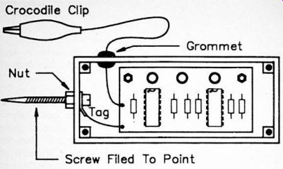
Fig.3.1 General arrangement used in probe type test gear.
A probe type piece of test equipment is really just an extension of the screened test leads idea. Probe tools usually take the general form outlined in Figure 3.1. The metal prod at the front of the unit is the non-earthy input, and an earth lead plus clip connect to the chassis of the equipment under test in the usual manner. Instead of having the signal coupled to the main circuit via a screened lead, the circuit is included in the probe assembly. As a result of this there are no long connecting leads, no screened cables are required, and the capacitance of the screen lead is avoided.
Home Constructor Probes
There are definite advantages to probe style test equipment, but it has to be admitted that they can be a bit awkward to construct. There are numerous project cases available, but few are specifically designed for this type of application.
Some of the smaller ordinary cases can be used in probe style projects without too much difficulty. The main problem is in finding something to act as the prod at the front of the unit.
The method 1 have found to be the easiest is to use a long 6BA or M3 screw. A screw 25 millimeters long is about the shortest that is likely to be usable, and I would recommend the use of one about double this length if you can obtain it. In fact an even longer screw might prove useful for reaching connection points in inaccessible places, but the chances of obtaining one are probably not very good. A solder-tag fitted on the screw inside the case represents an easy way of making a connection to the screw. If you require the usual pointed style test prod, some careful filing of the screw should produce the desired result. However, file the screw once it has been fitted to the case, not beforehand otherwise you may find that it is impossible to fit the fixing nut on to the screw. Figure 3.1 illustrates this general method of assembly.
Of course, if you search through a few component catalogues you may well find one or two cases intended for probe type circuits, and complete with the prod section. Where possible it is probably best to use one of these, but these cases will not necessarily be the right size and shape for the circuit board you wish to fit into them.
Analog Probe
An analog probe is a simple voltage measuring tool for making quick checks on equipment. It would be possible to have a miniature moving coil meter built into the probe, or a small digital readout. Most units of this type have a simple LED display though, often with just a few LEDs indicating whether or not the input voltage is above certain threshold levels. This unit has ten LEDs which have threshold voltages of 1 to 10 volts with one volt increments between LEDs.
It has what is generally termed a "bargraph" display, although in this case it is not strictly speaking a true bargraph. The display operates in the "dot" mode, which means that only one LED at a time is switched on. If (say) the input potential is five volts, then l.e.d. number five will switch on, but LEDs one to four will be switched off. This is not quite such a clear indication as a true bargraph display, but it has the advantage of keeping the current consumption down to more manageable proportions. This is especially important for a probe circuit where the use of a large battery is obviously out of the question.
Although a voltmeter with a single 0 to 10 volt range and only 1 volt resolution might seem too restricted to be of any practical value, it should be kept in mind that many home constructor projects are powered from 5 to 9 volt supplies, and that precise voltage measurements are not required in many instances. Often you only need something like "is the test point at about half the supply voltage?", rather than the exact voltage to the nearest millivolt. A unit of this type is not a replacement for a good quality multimeter, but it is a useful little aid for quick checks on many types of circuit.
A useful feature of this unit is that it has a high input resistance of around 11 megohms. It is therefore a form of high resistance voltmeter, and as such it will place very little loading on the test points.
The Circuit
Refer to Figure 3.2 for the full circuit diagram of the analog probe. This is based on the popular LM3914N bargraph driver (IC2). This device contains a voltage reference, decoder and driver circuits for the display, in fact just about everything needed apart from the display. The latter is formed by LEDs D1 to DIO, which are ordinary panel mounting LEDs mounted in a row. The LED current is controlled by internal constant current generators, and these are controlled by discrete resistor R3. This sets the LED current at about 10 milliamps, which gives good LED brightness without giving the unit an excessive current consumption. Pin 9 of IC2 is wired to pin 11 in order to set the device to "dot" mode operation.
The LM3914N is quite sensitive, and in its normal operating mode it only requires an input of 1.2 volts in order to light the tenth LED of the display. The input impedance of the device is not very high though. Consequently, in this circuit it is preceded by an attenuator and a buffer amplifier based on IC1. VR1 is part of the attenuator, and it is adjusted to give the correct sensitivity. By using other values for R2 and VR1 it is possible to accommodate other full scale sensitivities. For example, with these components at a value of 470k it should be possible to set up VR1 for a full scale potential of 20 volts (which gives 2 volt resolution).
The current consumption of the circuit is about 7 milliamps under standby conditions, or about 17 milliamps when one of the display LEDs is activated. This can be supplied by a PP3 size 9 volt battery, although there may be some advantage in using a high power type, especially if the unit is likely to receive a great deal of use.
Construction
Details of the stripboard layout are provided in Figure 3.3.
This requires a board having 50 holes by 17 copper strips. This can conveniently be a piece cut from a standard 5 inch long stripboard. IC1 is a MOS input operational amplifier, and it therefore requires the usual anti-static handling precautions.
Although IC2 is not a MOS device, it is not particularly cheap either. Consequently, I would strongly urge the use of a socket for this component.
The board is somewhat larger than its ideal size, making it impossible to fit the unit into a really small case. One reason for this is that I used 5 millimeter LEDs in the display.
Although it would seem that these could be spaced two holes apart (5.08 millimeters), this is not possible. The body diameter of each LED is 5 millimeters, but there is a wider ring at the rear of the body to permit fixing into panel clips.
This enforces the use of three hole spacing.
With a little ingenuity it would probably be possible to redesign the board slightly in order to produce a more compact layout. Simply changing to a different type of LED, such as 3 millimeter diameter types, should permit the LED spacing to be reduced to 0.2 inches. Relocating C1 and the connection points to B1 - and S1 might permit a further contraction of the board. In fact its length could probably be reduced to well under 4 inches if really small size is of paramount importance.
The basics of probe construction have been covered previously. It is really a matter of using a little initiative, and making the most of the materials you can obtain. Ideally the board should be mounted in the case in such a position that D1 to D10 can protrude through holes drilled at suitable positions in the case. An alternative is to have them just below one panel of the case. A window for the LEDs to "look" through is then cut in the case above the LEDs. This window should be fitted with some red window material.
About the only way of fixing this material in place is to cut it substantially over-size, and to then glue it in place behind the panel cutout, being careful to only apply adhesive near to the edges of the material. Window material is often made from a fairly brittle grade of plastic, and due care needs to be exercised when cutting it.
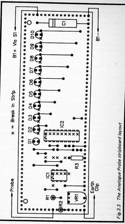
Figure 3.3
No wiring diagram is provided for this project, simply because there is very little point-to-point wiring. It is just a matter of wiring the board to the probe tip, the earth clip, the negative battery clip lead, and S1, and then connecting the positive battery lead to the otherwise unused tag of S1.
Components for Figure 3.2
Resistors (all 0.25 watt 5%) 10M R1 R2 1M R3 1-k2
Potentiometer
VR1 1M sub-min hor preset
Capacitor
C1 10u 25V axial elect
Semiconductors
CA3140E LM3914N Red LEDs (10 off) IC1 IC2 D1 to D10
Miscellaneous
B1 9 volt (PP3 size)
SPST sub-min toggle S1
Small case
Stripboard having 50 holes by 17 copper strips 8 pin DIL holder 18 pin DIL holder
Battery connector
Crocodile clip
Wire, solder, etc.
Calibration
With a resolution of only 1 volt the unit does not require any particularly precise calibration. Results will probably be satisfactory if the probe tip is temporarily wired to the positive supply rail of the unit, and VR1 is then adjusted to switch on D9. If you require optimum accuracy from the unit, you must provide an accurate calibration potential equal to a whole number of volts. For example, a project which has a stabilized 5 volt supply can be used to provide an accurate 5 volt calibration voltage. VR1 would then be adjusted to light up D5.
There will be a narrow range of settings over which this LED would switch on, and VR1 would be set as close as possible to the middle of this range.
It is worth reiterating here the dangers of making tests on mains powered equipment. You should certainly not do so unless you are quite sure you know exactly what you are doing. A unit of this type should never be used to make checks on equipment which has its chassis connected to one side of the mains supply.
CMOS Probe
In its most basic form a logic probe is a passive device using one or two LEDs to indicate the logic level at the test point.
While such a unit is very cheap and simple, it is not without some severe drawbacks. One of these is merely that the current needed to drive the LED or LEDs at reasonable brightness might be more than some logic outputs could reasonably be asked to supply. Most logic outputs are actually quite capable of driving a LED, but it has to be borne in mind that any outputs being tested may already be loaded to something approaching the maximum acceptable level.
Another drawback of a passive logic probe, and one shared by some of the more simple active probe designs, is that brief and infrequent pulses are unlikely to be detected. This is a major drawback as many logic circuits deal largely in signals of this type. A very brief signal will either fail to light the LED due to inadequacies in the switching speed of the LED, or in a less extreme case the LED will in fact pulse on, but the resultant flash will be too brief to be perceived by the human eye.
This active logic probe has three LEDs to indicate the logic state at the test point. Two of these LEDs merely indicate logic 0 and logic 1, as appropriate. If the input signal is a continuous pulse type of some form, then both LEDs will probably switch on. With an input signal having a 1 : 1 mark-space ratio the two LEDs will switch on at equal brightness. With any other mark-space ratio there will be a bias with the input signal spending more time at one logic level than the other. This is reflected in the brightness of the LEDs with the one having the input signal at its logic state for the greater amount of the time being brighter than the other LED Thus it is possible to roughly gauge the mark-space ratio of the input signal from the relative brightness of the LEDs. Of course, the input signal may not be a regular waveform, but the comparative brightness of these two LEDs will still indicate any bias towards one logic level or the other. As the bias varies, so will the relative brightness of the two LEDs.
The third LED is activated when an input pulse is detected.
Even if the input pulse is only very brief, the LED will still be switched on for around a second, so that a clear indication of the input pulse is provided. Thus, even with something like a 500ns pulse every two seconds, the third LED will clearly indicate each input pulse. It is possible (but unlikely) that the input signal could be between the maximum legal logic 0 voltage, and the minimum valid logic 1 level, and that this would cause the other two LEDs to switch on at about half brightness. Obviously the other two LEDs switched on at about half brightness could give the impression that the input signal was a pulse signal with a mark-space ratio of about 1:1. However, the absence of any indication from the third LED would show that no input pulses were present, and that the input signal was a static one at an invalid voltage.
This logic probe is based on CMOS integrated circuits, and is consequently only fully compatible with circuits that are based on 4000 series CMOS devices. In practice it will operate quite well with many TTL circuits, but it can not be guaranteed to do so. It is the higher speeds of TTL circuits rather than differences in logic 0/1 levels that are most likely to cause problems. Rather than taking the risk of getting misleading results by using this unit on TTL circuits, it would be better to build a separate TTL compatible probe. A suitable design is featured as the next project in this guide. Both the logic probes are so cheap that building both of them should not "break the bank"!
The Circuit
Figure 3.4 shows the full circuit diagram for the CMOS logic probe. IC1 is used at the front end of the circuit, and this is two gates from a 4001 BE quad 2 input NOR gate. The inputs of the two unused gates are tied to the positive supply rail in order to prevent spurious operations and to avoid any risk of damage by static charges. The two gates that are used are connected to operate as simple inverting buffer stages.
IC1a acts as a buffer at the input of the unit, and its input is normally connected to the 0 volt rail by R1. CMOS inputs should not be left floating, and it is therefore important to have this resistor to hold the input at a valid logic level (and provide static protection) under standby conditions. NOR gates are often connected as inverters by connecting both their inputs together, which is the method that has been adopted with IC1b. For IC1a the alternative of taking one input low and using the other as the input of the inverter has been used. This has the advantage of loading the test point by a single CMOS input rather than by two inputs.
Fan-out is not usually a problem with CMOS logic devices, where it is usually possible for a single output to drive fifty or more inputs. However, as with any test equipment that taps-off some signal from the circuit under test, loading is something which must always be borne in mind. D1 switches on when the input is low (logic 0), and D2 switches on when the input is high (logic 1).
Pulse detection is provided by IC2, which is a CMOS 4047BE monostable/astable. In this case it is connected in the positive triggered monostable mode. In this application it does not really matter whether the unit is triggered on positive going or negative going edges, since any input pulse will have both types of transition and will trigger the circuit. 1C2 is used in the non-retriggerable mode, and this is an important factor. With a retriggerable monostable, holding the input at the appropriate logic level has the effect of extending the output pulse indefinitely. This could obviously give confusing results, with a static input giving the impression that input pulses are present. A non-retriggerable monostable can only be triggered by a transition of the appropriate type. The output pulse always ends after the appropriate period of time regardless of what logic level is present at its input during that time. Once the output pulse has finished, only another transition of the correct type will trigger the circuit again.
This ensures that LED indicator D3 is only triggered when there is an input pulse. C1 and R4 set the flash duration for D3, and the specific values give a duration of very roughly one second. If a shorter flash is preferred, simply make R4 lower in value (the output pulse duration is proportional to the value of this component).
The unit is powered from the circuit under test, and a second crocodile clip lead is included to permit the +5 volt line to be "tapped". The unit could be powered from an internal battery supply, but I would advise against this. Apart from the battery adding bulk and weight to the unit, you should remember that not all CMOS logic circuits operate from a standard 5 volt supply. Most do, but there are plenty of CMOS circuits operating at various supply voltages from 3 to about 15 volts. The probe will not function properly if there is a mismatch in the supply voltages, and there would be a slight risk of the probe being damaged when testing circuits with a supply voltage of more than 5 volts. Powering the unit from the circuit under test is an easy way of avoiding any supply mismatch problems. Of course, the unit under test must be capable of providing the extra current, but in most cases it should be well able to do so. From a 5 volt supply the unit draws only about 4 milliamps with one LED activated, or about double this with two LEDs switched on.
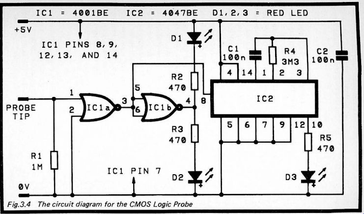
Fig. 3.4
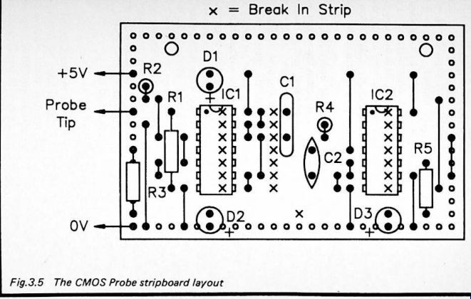
Fig. 3.5
Construction
Figure 3.5 shows the stripboard layout for the CMOS logic probe. It is based on a board having 26 holes by 16 copper strips. There is little out of the ordinary about construction of the board, but both integrated circuits are CMOS types, and they therefore require the standard anti-static handling precautions. One input of 1C2 lacks any built-in protection circuits, and I would recommend that the handling precautions are scrupulously observed with this component, even if you do not normally bother too much about them.
Although D1, D2, and D3 are shown as being mounted on the board in Figure 3.5, it is of course quite in order to mount them off-board in panel holders if preferred. I would strongly urge the use of high brightness LEDs, since the LED current is quite low when the unit is used with low voltage supplies of around 5 volts. You may like to use LEDs of different colors so that the display is easily interpreted even when just quickly glancing at it. The method of denoting the cathode (+) leadout of LEDs varies, but by far the most popular method is to have the cathode lead shorter than the anode one. Also, the cathode leadout is usually much thicker than the anode one close to the body of the component. If necessary you can use trial and error to find the right method of connection.
Connecting a LED the wrong way round should not result in any damage to the component.
Components for Figure 3.4
Resistors (all 0.25 watt 5%)
1M R1 470
R2 R3 470 3M3 R4 470 R5
Capacitors
100 nF polyester (C280) 100 nF ceramic C1 C2
Semiconductors 4001 BE 4047BE
Red LED
Red LED
Red LED
IC1 IC2
D1 D2 D3
Miscellaneous
Small case
Stripboard having 26 holes by 16 copper strips
Two 14 pin DIL holders
Two crocodile clips
Wire, solder, etc.
In Use
The first step when using the unit is to connect the two power supply leads. It is not usually too difficult to find suitable connection points on the circuit under test. If necessary, a couple of short (non-insulated) leads can be soldered to the circuit board of the unit being tested so as to provide suitable take-off points. Be very careful to get the supply leads round the right way. It is a good idea to use red and black leads so that it is very obvious as to which lead is which.
Very often you will notice D3 flash when the probe tip is connected to a test point, and when it is removed again.
This is due to an input transition as the probe is connected and disconnected, and does not necessarily indicate a pulse at the test point. In order to be sure that the test point is pulsing you must wait until the end of any initial flash from D3, and any subsequent flash from D3 should be a valid indication. However, be careful to hold the probe tip firmly on the test points. Bad or intermittent connections are almost certain to generate spurious input pulses.
The table on page 101 summarizes the LED states for various types of input signal.
---------
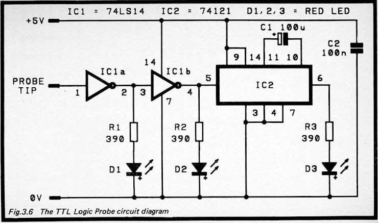
Fig. 3.6
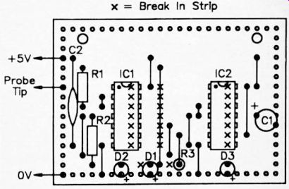
Fig.3.7
The stripboard layout for the TTL Logic Probe
TTL Probe
The circuit diagram for the TTL logic probe appears in Figure 3.6. This is not an exact equivalent to the CMOS version, as it has a rather different input section based on inverters rather than NOR gates. It is essentially the same though, with Dl, D2, and D3 providing the same functions as their counterparts in the CMOS probe circuit,
The monostable is based on a 74121 (IC2), and use is made of the internal timing resistor. Consequently, if you wish to shorten the output pulse duration to provide briefer flashes from D3, this must be achieved by making C1 lower in value.
Figure 3.7 shows the stripboard layout for the unit, and this is based on a board having 23 holes by 16 copper strips.
Construction of the board is very straightforward, although the compactness of the layout means that extra care must be taken to avoid short circuits between copper strips due to solder splashes. Neither IC1 nor IC2 require any special handling precautions, but it would still be a good idea to use sockets for these components.
The notes on using the CMOS probe apply equally to the TTL version, and the points on use made previously will not be repeated here. The unit provides loading on the test point equal to one LS TTL input (or one standard TTL input if a 7414 is used in the IC1 position). No input resistor is needed with the TTL probe as there is no risk of damage due to static charges, and the input will always float high. Note that the unit differs in this respect from the CMOS version, where the input is taken low under standby conditions.
Components for Figure 3.6
Resistors (all 0.25 watt 5%) 390 R1 390 R2 390 R3
Capacitors
100u 10V radial elect 100n ceramic
C1 C2
Semiconductors
74LS14 74121
Red LED
Red LED
Red LED
IC1 IC2 D1 D2 D3
Miscellaneous
Small case
Stripboard having 23 holes by 16 copper strips
Two 14 pin DIL holders
Two crocodile clips
Wire, solder, etc.