Pulse modulator provides switched-mode amplification
by P. H. Pazov Polytechnic of Central London, England
Using pulse-width modulation to provide switched-mode amplification, this circuit affords the same advantages in the analog world as does its switching power supply counterpart--simplicity, efficiency, and low power consumption when a complementary-MOS logic family is employed. Noise rejection and distortion characteristics also are better than can be achieved with a conventional analog arrangement.
As shown in the general function diagram (a), a feedback current, Imod, is derived from the audio input signal for the purpose of varying the pulse width of a free-running oscillator, which itself is formed by a digital integrated-circuit integrator and a hysteresis/power stage. C2 and R4 develop a dc feedback signal from comparison of with the audio input, from which an error current is created. The ratio of R4/R5 sets the amplification factor. C2 and C3 act to integrate so that any long-term imbalance appears as an error and can be corrected.
The active digital elements thus switch in the linear mode, ensuring that the output pulse width is proportion al to the amplitude of the input signal. The output, as taken at the junction of L and Co, represents the instantaneous change in the oscillator's pulse width. With such an arrangement, the amplifier's efficiency is better than 90% at any signal level, as would be expected with any linear switched circuit.
The practical implementation is shown in (b). One 4049 inverter is used for all switching functions. C2 and R4 set the total bandwidth at about 20 kilohertz, with C3 determining the lower cutoff frequency of 100 hertz. The circuit has an amplification factor of 15. It will drive a load as low as 2 ohms at a noise level that appears low enough for headphone-monitoring applications. With a supply voltage of 6 volts, the current consumption will be a mere 5.6 milliamperes.
As mentioned, the circuit's noise performance is very good. This is partly due to the fact that, as the modulation current increases toward the maximum charging current required to attain the maximum pulse width in the oscillator, a form of frequency modulation occurs, giving rise to an S-shaped transfer curve that is characteristic of an fm discriminator. This characteristic results in a lower noise and distortion factor than can be achieved using a purely linear approach.
As with all high-frequency circuits, a good earth ground and no ground loops are essential to proper operation. Otherwise, all sorts of oscillations appear and add to the noise level.
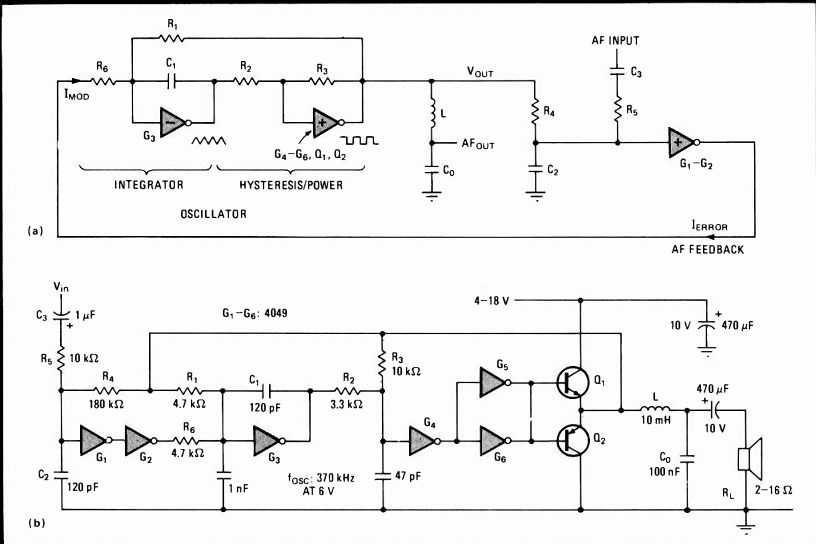
Linear logic. This digitally switched network (a) amplifies audio signals linearly by modulating the pulse width of an RC oscillator. The practical circuit (b) is uncomplicated. Excellent noise-rejection performance is achieved by the modulator's S-shaped transfer curve.
Antilog amplifiers improve biomedical signal's S/N ratio
by T. G. Barnett and D. L. Wingate London Hospital Medical College, Department of Physiology, England
Low-voltage, biphasic signals recorded by instruments monitoring biomedical variables such as heart rate are often accompanied by high noise levels due to inadequate sensing, movement artifact, paging systems and power-line interference. Using paired antilogarithmic amplifiers, however, to provide the nonlinear amplification required, the level of the biphasic signals can be raised well above the amplitude of the interfering signals. The signal-to-noise ratio can thus be improved from 2:1 at the input to 10:1 at the output.
Such a scheme is superior to the use of paired logarithmic amps, which cannot handle biphasic signals at the zero-crossing points (log 0 = co), and provides more sensitivity than conventional diode clippers, which intro duce noise and cannot pass signals that drop below the circuit's 0.7 clipping threshold.
Input signals are amplified by A1 and are separated into their positive and negative components by precision half-wave rectifier A2 and inverter A3. The corresponding outputs are then introduced into the AD759N and AD759P log/antilog amplifiers, which are wired to yield e0 = Eref10^e_in1.-/K for-2 –e^in1/K<=2, where Era is an internal reference voltage of approximately 0.1 volt and K is a multiplying constant that has been set at 1 as a consequence of utilizing input e_in1. The output voltages generated by A4 and A5 are of negative and positive polarity, respectively.
These components are then summed by A6, whose output yields a bipolar, anti-logged signal that can be introduced to appropriate trigger circuits. If desired, the original signal can be reconstructed by passing it through paired logarithmic amplifiers.
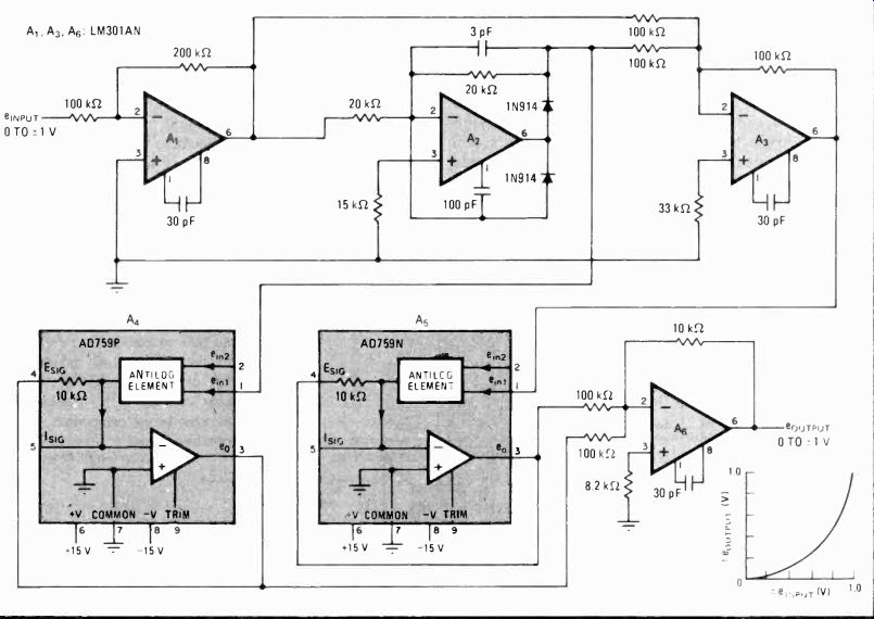
------- Biomedical booster. Paired AD759 antilog amps provide bipolar,
nonlinear amplification, thus raising level of biphasic signals such
as EKGs with respect to noise and so increasing S/N ratio. Circuit is
superior to those using log amps, which cannot provide accurate output
at zero crossings of signals, and is more sensitive than diode clippers,
provides greater noise rejection than filters, and introduces no phase
shift.
Bilateral speaker networks form switchless intercom
by Frank Kasparec St. Poelten, Austria
Only one transducer-a dynamic loudspeaker-is required at each station of this intercom to permit transfer of audio information in both directions simultaneously. Having no need for push-to-talk switches, the circuit is less costly and less bulky than conventional transceiver units. Undesired acoustic distortion normally encountered in this type of transmission system is eliminated by using a simple phase-compensation network.
As described for the receiver portion of the unit, audio signals at the input are converted into their acoustical equivalent, S1, by the speaker after passing through the RC network made up of C1 and resistors R3 to R7, which is required to offset the frequency-dependent phase shift created by the speaker's inductance. When properly set, potentiometer R6 also cancels the feedback (talkback) voltage appearing at the noninverting input of the 741 differential amplifier, which is normally used to amplify the electrical equivalent of the acoustic vibrations, S2, hitting the cone of the speaker in the transmit mode.
As expected, the compensation network responds similarly to voltages emanating from the speaker's coil, acting to minimize phase distortion at V.. In this case, however, input signals to the differential amplifier are in the millivolt range. The 741 op amp provides a gain of R9/R8 and thus the needed amplification at V. Note that in most cases a power stage will be required following the 741 op amp to energize a loudspeaker.
The design of the phase-shift network, although easy, must be done with care if acoustic feedback is to be reduced to a minimum. The phase differences as seen by the differential amplifier must be canceled, and thus (R1 + R2)/Z1 = Zo/(R3+ R4/2), where:
Z1 = jXL1, Zci is the reactance of capacitor C1, and L1 is the speaker's inductance. It is also assumed that R2 is approximately equal to R1. and R3 and R4 are much smaller than R5-R7. For the general purpose speaker, R1 will be about 4 or 8 ohms. The above equation reduces to (R1 + R2) (R3+ R4/2) = L1/C1. At the same time, for direct current balance at the output of the op-amp, R2/R1 = (R7 + R6/2)/(R5 + R6/2).
To determine the element values in the phase-compensation network, and to estimate the frequency response of the unit, it is necessary to measure both the loud speaker's dc resistance and its inductance. The best way to find the dc resistance is to use a digital ohmmeter. To determine coil inductance, it is necessary to apply an audio signal (preferably at f = 1 kHz) to the loudspeaker, as shown in the inset, and to measure A, the ratio of the root-mean-square output voltage to the rms input voltage. The coil inductance is then given by:
LI = [R12- A2(R, + R2)2/47r2P(A2-1)V
Rearranging the equation:
A = [R12+ 4...2f2L2/(R1 + R2)2+ 4,2f2L2] /2 and it can be seen that the speaker response tends toward a high-pass characteristic. Because L1 is generally negligible, the frequency response is largely flat over the audio range.
Adjustment of the circuit is simple. R4 is initially set to null the output of the differential amp under no-signal conditions. A square wave is then applied at V, and R6 set to minimize V..
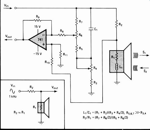
Double duty. One-transducer intercom station using dynamic loudspeaker minimizes cost and bulk of conventional units. Compensation network (R3-R7)C, reduces phase distortion created by speaker. Speaker inductance may be easily measured (see inset) in order to set component values in compensation network.
TTL line drivers link fiber optics
by Vernon P. O'Neil and Imre Gorgenyi Motorola Inc., Discrete Semiconductor Division, Phoenix, Ariz.
Designers who need to convert an existing twisted-pair communications interface into an optical-fiber link can minimize their efforts by simply combining their fiber optic detector-preamplifiers with TTL line receivers like the industry-standard MC75107 devices. Such an arrangement has other advantages besides simplicity, namely, providing the builder with access to two receivers, complete with strobing inputs, in a single 75107.
And although no similar optical line receivers are yet offered as a standard product, this interface will yield good performance at low cost. Building fiber-optic transmitters using TTL line drivers is equally simple.
The union of the 75107 with Motorola's MFOD404F optical detector is shown in (a) of the figure. The detector is packaged in a nose-cone type of fixture that can be directly mounted in standard AMP-connector bushings, making the connection to the optical-fiber cables extremely simple.
The resulting optical receiver will handle data rates of up to 10 megabits per second at a sensitivity as low as 1 microwatt. For even greater data rates, an MFOD405F can be used to extend the data-rate capacity to 50 Mb/s at a sensitivity of 6µw.
Because the receiver is ac-coupled to the detector, it is necessary to restrict the duty cycle of incoming signals to the range of 40% to 60%. Coupling components between the detector and the 75107 are selected to ensure that the reference level developed at the input of the receiver tracks the average voltage of the input data stream. In this way the circuit self-adjusts to a wide range of input optical power levels.
At the other end of the system (b), a compatible ac-coupled optical transmitter can be constructed from an ordinary 75452 line driver. A 0-to-2-Mb/s fiber-optic transmitter suitable for handling bipolar-pulse (dc-coupled) encoded data (c) is almost as simple.
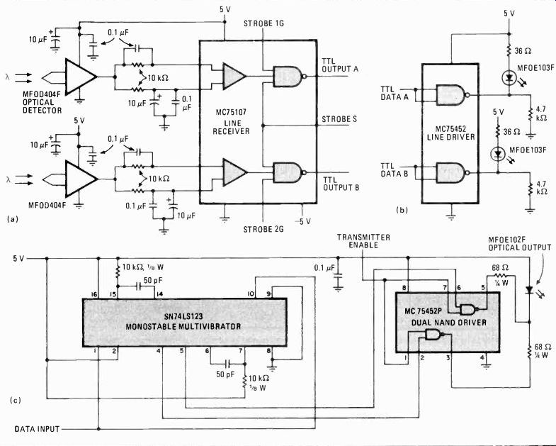
------ Light line. Standard line receivers such as the 75107 serve
well in interface for fiber-optic systems (a). Off-the-shelf TTL line
drivers at the transmitting end (b) makes possible low-cost systems.
A 0-to-2-Mb/s bipolar-pulse-encoded transmitter (c) is almost as simple
to build.
Dc-coupled trigger updates quickly
by Andrzej M. Cisek Electronics for Medicine, Honeywell Inc., Pleasantville, N. Y.
Two operational amplifiers and a few components build this broadband trigger, which is absolutely immune to the problems created by dc offset and base-line wandering. A self-adapting stage for maintaining a constant level of hysteresis, as well as dc coupling at the input, permits a low-cost yet superior performance over a wide range of input signals that makes the circuit very attractive for biomedical applications.
Input signals are applied to the LM307 amplifier, A1, through charge-storage network D1D2RIR2C (a). Diodes D1 and D2 quickly charge capacitor C to the peak of the input voltage (less one diode drop) and minimize C's discharge until the signal falls more than two diode drops below the peak voltage.
The output of A1 is then compared with the original signal at A2. The amount of hysteresis is set by constant-current source Q1 and Q2, two p-channel field-effect transistors wired as diodes in A2's positive feedback loop, and R3. Q1 and Q2 ensure that the level of hysteresis is maintained virtually constant for any dc offset at the input. Resistor R1 provides a zero level for input signals whose amplitude is smaller than one diode drop, and R2 protects the input-signal source.
Such an arrangement has a reliable triggering level and responds fast, its speed being limited only by time constant (RD1,2 + R2)C. This time constant can be easily adjusted to meet the requirements of practically any application.
As for the circuit's use in medical electronics, consider the two cases illustrated in (b) and (c), where a cardiac signal representing heart rate is superimposed on the respiratory (breath) signal. Depending on the trigger level, either heart rate (b) or respiration rate (c) may be counted.
-------- Flat. Trigger (a) maintains switching level over a wide
band of frequencies and Input-signal amplitudes. Operation is independent
of input dc offset and problems created by baseline shift. Directly coupled
arrangement at input contributes to circuit's high-speed response. In
biomedical application, trigger switches on superimposed signals produced
by heart rate (b) and respiration rate (c).
Optical agc minimizes video measurement errors
by D. Sporea and N. Miron National Center of Physics, Magurele, Rumania
In an optical system, pulse width and peak amplitude are two information-bearing parameters that must be measured accurately for intensity-distribution and frequency-domain analysis-parameters that are difficult to determine when variations occur in the intensity of the signal's laser light source. This difficulty may be virtually eliminated by using the unmodulated laser signal to provide automatic gain control of the amplifier that processes the optical signal from a video camera. Such a scheme rejects the black level of the optical input signal, minimizes drift of low-level detector thresholds, and reduces noise caused by light scattering through optical components for near-zero level signals.
Signals are applied in a balanced fashion to the IA733 video amplifier, as shown. R1C1, R2C2, and the excellent common-mode characteristics of the operational amplifier reject most optical noise and bias the black level below the amplifier's active region.
The gain is controlled by a phototransistor operating in its linear region and two field-effect transistors whose drain-to-source resistance varies directly as a function of the reference laser signal. If the laser power increases, amplifier gain will be proportionally lowered, and vice versa, so that the output amplitude for a given video signal will be relatively independent of changes in the reference level. The signal is then amplified by the µA715 operational amplifier and presented to the µA710 high-speed comparator, where the switching threshold is set by the user.
In operation, the circuit provides excellent agc characteristics. Typically, the peak voltage (Vs) at the output of the 715 (see inset) will vary only 0.35 decibel for a given video signal and a change in laser input power of more than 10 dB. The roll-off response of filters R1C1 and R2C2 is such that the detector's threshold voltage, Vt, varies to a similar degree. Consequently, the ratio of VP/Vb is virtually unchanged, a condition required for accurate measurements of width versus intensity.
---------- Lightbeam leveler. Phototransistor sets gain of input
amplifier, ensuring that variations in output power of unmodulated laser
light source have little effect on pulse-width measurements of optical
input signal, which is derived from video camera. Change in output amplitude
is only 0.35 dB for laser-power variations of more than 10 dB. Detector's
threshold voltage varies to a similar degree.
Differential amp cancels integrator's crosstalk
by Elzbieta Nowicka Atomic Energy of Canada Ltd., Ottawa
The performance of a high-speed integrator can be improved considerably by utilizing the excellent common-mode rejection characteristics of an operational amplifier to reduce crosstalk caused by the switching of waveforms during the circuit's integrate-and-hold sequence. More specifically, operating the amp in its differential mode enables the integrator to virtually cancel the switching offsets that are generated by the almost ideal switch-the complementary-MOS analog gate, which is inexpensive and has low on-resistance but relatively high feedthrough. The supporting circuitry required (two extra gates) is minimal.
The technique generally used to start and terminate the three-step integration sequence is shown in (a), where S1 and S2 represent two electronic switches. These switches must be selected carefully, the main requirement being that the on-resistance of these devices be as low as possible, especially when the RIC, time constant is small.
The c-mos CD4066 transmission gate, with its nominal on-resistance of only 80 ohms for a supply voltage of 15 volts, would normally serve well in these applications, except that its crosstalk (the unwanted feedthrough of the gating signal) is high-typically, 50 millivolts for a 10-v square wave having tr = tr = 20 nanoseconds and a gate-output load of 1 kilohm. By introducing a pair of switches at each of both inputs of the LM218 op amp (b), however, the integrator will provide virtual elimination of the crosstalk by means of differential cancelation of gate feedthrough signals 1 and 2. There will be little error introduced by the differences between the on resistance of each individual gate in the 4066 package because of the balanced circuit arrangement. Typically, Aor, will be less than 5 ohm for a 15-v supply.
Utilizing this scheme, the crosstalk will be reduced to less than 3 my over a temperature range of 0° to 70°C.
----------- Negated. Op amp virtually eliminates crosstalk of analog
gates in switching integrator by using differential-input cancelation
method.
Nominal crosstalk becomes 3 mV, sharply reduced from gate's typical value of 50 mV. Differences in on-resistance characteristics of individual gates in package introduce little error.
On-chip transistors extend audio amp's design flexibility
by Jim Williams National Semiconductor Corp., Santa Clara, Calif.
The availability of extremely low-cost audio-amplifier integrated circuits with on-chip transistor arrays, such as National's LM389, gives designers a great deal of flexibility in designing audio circuits. They make it much easier to develop low-cost versions of circuits unrelated to basic audio amplification, such as dc-dc converters, touch switches, stabilized frequency standards, scope calibrators, low-distortion oscillators, and logarithmic amplifiers. The designs of the often-needed converter, a bistable touch switch, and a tuning-fork frequency standard are discussed here in the first part of this two-part presentation.
The LM389 contains a 250-milliwatt audio amplifier and an array of three npn transistors, each of which is uncommitted. The amp has differential inputs and separate pins for setting its gain (from 20 to 200) via a resistor and runs off a single supply that may range from 4 to 15 volts. The three transistors have a minimum current-handling capability of 25 milliamperes and a minimum current gain of 100 for V,,, = 12 v and for a wide range of collector currents. The chip is therefore ideal for general use.
One area in which the chip will be useful is in dc-dc switching conversion. The device in Fig. 1 is intended for use as a power supply in a digital system where it is necessary to supply ±15 V to a low-power load. As can be seen from the oscilloscope photograph, the LM389 switches at 20 kilohertz. That rate is determined by the triangular-wave feedback signal, whose time constant is set by R1C,C2, and its square-wave output is applied to transistors Q1 and Q3. The series diodes ensure clean turn-off for Q1 and Q3.
Q1's inverted output drives one half of the transformer primary through Q2, while Q3 drives the other half. The diodes across Q2 and Q3 suppress spikes. Thus there is an efficient step-up of voltage across T2. This ac signal is rectified and filtered to produce complementary output voltages that may be used to power the desired linear components, in this case delivering ± 1.5 mA, enough to power an operational or instrumentation amplifier.
The bistable touch switch (Fig. 2) allows a line-powered load to be controlled from a touch plate by means of a thyristor. Each time the plate is contacted, emitter-follower Q1 conducts, permitting a fraction of the 60-hertz input signal to be applied to the inverting input of the amplifier. Consequently, the normally high output of the op amp follows the 60-Hz line input, causing V, to drop sharply.
This negative transition triggers a toggling flip-flop formed by Q2 and Q3. In this manner, the output of the flip-flop changes state each time the touch plate is contacted, prompting the firing of the silicon controlled rectifier or triac that switches ac power to the load.
Figure 3 shows a tuning-fork frequency standard that is stabilized by appropriate feedback. Both sine-wave and Tit-compatible outputs are available. As the circuit needs only 5 v, it can run off a battery.
The tuning fork proper supplies a low-frequency output that is very stable (typically to within 5 ppm/°C) and has an initial accuracy of within 0.01%. Moreover, it will withstand vibration and shock that would fracture a quartz crystal. Here, Q3 is set up in a feedback configuration that forces the fork to oscillate at its resonant frequency. Q3's output is squared up by Q1 and Q2, which provide a Tit-compatible output. When passed through an LC filter and the op amp, which provides a low-impedance (8-ohm) output, the signal is converted into a sine wave having less than 1% distortion, as shown in the figure.
Several other useful circuits also can be built. The second part of this article will deal with the chip's use in a portable scope calibrator, a low-distortion oscillator, and as a logarithmic amplifier.
--------- 1. Condensed converter. Op amps with an on-chip transistor
array, such as National's LM389, make Inexpensive one-chip switching
converters. Costing under $10, unit shown provides ± 1.5 mA at ± 15 V
for Instrumentation amplifier. Scope photo displays waveforms at various
points in circuit.
Use of diodes in driver side of circuit allows spike suppression, plus clean switching.
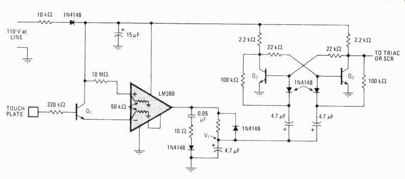
--------- 2. Simple switching. Simple bistable touch switch may be
similarly constructed. Op amp works as comparator and trigger for flip-flop
02-03, which changes state each time plate is contacted. Thus, SCR at
output may be alternately fired and switched off on command.
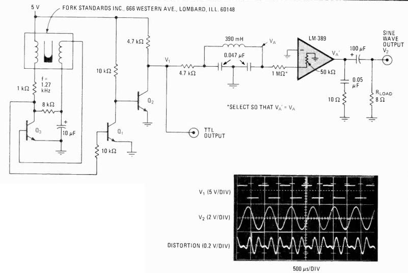
------------- 3. Stabilized standard. Tuning-fork frequency standard
uses 0, and Q2 to provide TTL output of waveform stabilized by 03 and
its associated components, which comprise the feedback network. Op amp
serves as butter for square-wave signal, which is converted into a sine-wave
output having 0.1% distortion after passing through the low-pass filter.
Initial accuracy is to within 0.01%, and drift is less than 5 ppm/°C.
On-chip transistors add versatility to op amp
by Jim Williams National Semiconductor Corp., Santa Clara, Calif.
Low-cost audio-amplifier chips containing uncommitted transistor arrays are widely applicable, as discussed in part 1 of this article [Electronics, Jan. 27, 1981, p. 118].
Besides uses in nonaudio applications such as dc-dc converters, touch switches, and stabilized frequency standards, array amplifiers like National's LM 389 are especially suited for general service in portable oscilloscope calibrators, low-distortion oscillators, and logarithmic amplifiers.
For example, the circuit in Fig. 1 allows a quick check of an oscilloscope's time base and vertical calibration. It can be built into a small hand-held enclosure and may be powered by a 12.5-volt battery.
When suitably trimmed, the amplifier will oscillate at 1 kilohertz ± 5 hertz. Transistor Q1 serves as a switch to provide fast, sharp edges to Q2's base. This transistor drives Q3, which functions as a zener diode so that a relatively constant 10-v square wave is applied across the resistive divider at the output. Q3's breakdown potential is scaled by the 2-kilohm potentiometer to provide a 5-, a 1-, and a 0.1-v square wave at the appropriate output taps. Loading of the circuit by a 1-megohm oscilloscope impedance will not introduce any appreciable error.
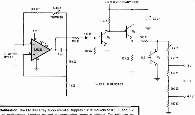
--------- 1. Calibration. The LM 389 array audio amplifier supplies
1-kHz markers at 0.1, 1, and 5 V for an oscilloscope. Loading caused
by connecting scope is minimal. The unit can be comfortably powered by
a 12-V battery for field applications.
In Fig. 2, the LM389 is called on to provide a low-distortion sine wave and a synchronous in-phase square wave. The circuit's 0.25-watt output capability enables it to drive such loads as a transducer bridge. In such an application, the in-phase square-wave output can be used to drive a set of synchronous demodulation switches.
The oscillator's low distortion (0.2%) is directly trace able to the use of a light bulb that provides smooth amplitude-limiting for the Wien-bridge network of the amplifier. The oscillation frequency is 1 kHz. The in-phase square-wave output is ensured by Q,-Q3 and the potentiometer R1, with Q2 and Q3 speeding up the waveform's edges. Calibration for synchronism is simply performed by adjusting R1 so that the edges of the square wave line up precisely with the zero-crossings of the sine-wave output.
As shown in Fig. 3, the LM389 is used in an unorthodox fashion to build a logarithmic amplifier that eliminates the complex and expensive means by which temperature compensation is usually achieved. Thus, the cost of the log amp is reduced by some 90% compared with that of conventional approaches.
Q2-Q3 operate in a heat-generating and-sensing feed back network, with Q2 serving as the heater and Q3 the temperature sensor. This combination keeps the temperature virtually constant, so that the LF353 op amp's transfer function, as determined solely by logging transistor Q1 and the 1N4148 diode, will be independent of any variation in temperature.
When power is first applied, Q2's emitter voltage rises to about 3.3 v and a current of 120 milliamperes flows.
This current forces Q2 to dissipate about 1.5 w, which raises the chip to operating temperature very rapidly because of its small size. At this time, the thermal servo Q2-Q3 takes over, because the LM389 senses the dependence of Q3's base-to-emitter voltage drop on temperature and drives Q2 to a temperature (50°C) corresponding to the setting of the 10-kO-to-1-1d1 divider string.
Since the LM340 never has a voltage of more than 3 v across it, the power dissipation never exceeds 0.3 w.
Note that the zener diode at the base of Q2 will prevent servo lock-up when the circuit is initialized.
Since the LM340 never has a voltage of more than 3 v across it, the power dissipation never exceeds 0.3 w.
Note that the zener diode at the base of Q2 will prevent servo lock-up when the circuit is initialized.
To calibrate the temperature servo, the base of Q2 must first be grounded. The collector potential of Q3 must then be measured at a known room temperature.
Calculate what Q3's potential should be at 50°C, assuming a temperature coefficient of- 2.2 millivolts/°C.
Next, trim the 1-kg resistor in the resistive divider so that the voltage at the LM389's inverting port approximates the calculated potential. Finally, unground Q2's base. The Q2-Q3 servo loop should then be functional. As a check, note Q3's collector voltage stability (within 100 ture and drives Q2 to a temperature (50°C) correspond- my) and temperature change (0.05°C maximum) as cooling to the setting of the 10-k0-to-1-1d1 divider string. air is applied to the LM389.
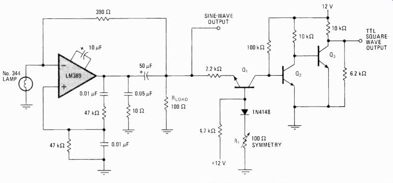
-------- 2. Sines and squares. This oscillator provides a 1-kHz
sine-wave output and synchronous in-phase square waves. The amplitude-limited
Wien bridge contributes to low distortion (0.2%). Single-knob calibration
for synchronization is provided by potentiometer R1.
--------- 3. Holding heat. The LM389's servo loop, Q2-03, performs
low-cost temperature compensation for the LF353 op amp, which is configured
as a logarithmic amplifier. The chip temperature, initially determined
by current through 02, is set with the 1-kf2-to-10-kf2 resistive divider.
Integrator improves 555 pulse-width modulator
by Larry Korba Ottawa, Ont., Canada
In one method of providing linear pulse-width modulation with the 555 timer, a current source charges a timing capacitor, creating a ramp signal that drives the modulation input of the 555. Unfortunately, the circuit offers only a limited dynamic range of pulse widths and is highly sensitive to temperature. A better way is to use a resettable integrator as the timing element.
Charging with a constant current source (a) at best yields a 2:1 dynamic range for a supply of 5 volts-the linear operating range for voltage-to-pulse-width con version is approximately 2.1 to 4.1 v, and the timing capacitor is totally discharged every timing cycle. Furthermore, the circuit requires temperature compensation to eliminate any timing fluctuation due to the tempera ture sensitivity of Q1, since the base-emitter voltage varies at the relatively high rate of-5 millivolts per °C.
And, to add to the circuit's woes, Icbo varies with temperature as well.
The resettable integrator (b) made up of A2, Q1, C, and R applies a trigger pulse to the 555, causing Q1 to turn off. Integrator A2 then ramps up until the voltage level at the modulation input of the timer equals that at pin 5. When that happens, Q1 is turned on again, reset ting the integrator and turning off the 555.
The voltage applied to the integrator, V is set to 2.1 v. This makes the shortest linearly modulated pulse width equal to the trigger pulse width-2 microseconds.
With the timing values shown, the maximum pulse width is 6 milliseconds, producing a dynamic range of more than 3,000:1 over the linear operating region.
The active components affecting the timing circuit are A2, Q1, A1, and V. Since the average temperature coefficient for the offset voltage of A2 is a very low 5 microvolts/°C (affecting the timing by only 2.5 parts per million/°C), the circuit's almost negligible adverse temperature effects are largely due to the variation with temperature of the off current of Q,, Ids,. Ichs doubles every 10°C; for the 2N4360, it is about 10 nano-amperes at room temperature.
It is important to note that for both circuits, the effects of Vcc and the 555 on timing stability are the same. As a bonus, however, the new circuit provides a linear ramp output that can be loaded fairly heavily without seriously affecting circuit timing.
---- Old style, new style. In the most common method of linear pulse-
width modulation using the 555 timer integrated circuit (a), the timing elements are current source Q, and capacitor C. The sensitivity of the pulse characteristics to circuit parameters leaves much to be desired.
When a resettable integrator is used to time the modulator (b), circuit sensitivities are reduced greatly. As a bonus, pin 6 provides a ramp output with significant drive capability.
WAVE FORMS AT A1 t +12 V
Bi-FET op amps simplify AGC threshold design by John H. Davis Warm Springs, Ga.
---------1. Easy play. Only one adjustment to zero the output of the
TL071 op amp under no-signal conditions is needed in this AGC threshold
amp.
Good performance is achieved by using the amp's common-mode properties. The control voltage must vary from zero to a negative value.
---------- 2. Simpler. Threshold detection, time constants, and amplification
are consolidated in this single stage. For a receiver's i-f strip, an
emitter follower is recommended, however. The control voltage here varies
from a fixed negative value toward zero.
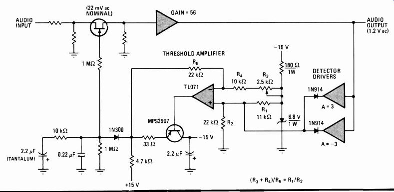
Operational amplifiers with the bandwidth and input impedance available using bipolar-field-effect-transistor (bi-FET) technology are well suited for integrating the threshold detection and automatic-gain-control amplification functions in audio limiters or receiver AGC circuits. Generally, such circuits are implemented with discrete components. But this often entails component selection and critical trimming adjustments, or both. An op amp approach makes an AGC design more predict able, stable, and easier to troubleshoot.
The circuit of Fig. 1 requires only one adjustment, to zero the output of the TL071 op amp under no-signal conditions. In this circuit, a control voltage is required over the range from zero (at full gain) to the negative value corresponding to the FET's cutoff voltage. A zener diode supplies the reference voltage. It is connected in a way that makes use of the common-mode rejection properties of the op amp; thus, R3 nulls the static output, which thereafter is quite stable.
The threshold is the voltage appearing at the junction of R1 and R2, plus the forward drop of the detector diodes, and can be readily computed for any desired limiting level. For the detected peaks, the threshold detector has a voltage gain of:
Ade, = (R1 + R2)/R1
Not much gain is ordinarily required; too much imposes tighter tolerances on driver gain, diode properties, and trimmer adjustment. Driver gain can be adjusted, within output swing limits, to tailor limiting slopes.
The emitter follower improves the attack time of the time constant network. The dual set of time constants shown prevents short-duration peaks from depressing system gain longer than necessary.
Further simplification (Fig. 2) is possible if the driver amplifiers have low output impedance. Here the threshold detection, time constants, and amplification are consolidated in a single stage. This consolidation around one op amp means that little additional circuitry is needed when an FET is the voltage-controlled element.
The circuit assumes the control voltage must vary from a fixed negative value toward zero as gain reduction is needed. With no signal, the threshold op amp is referenced to the desired voltage by the zener diode. As long as no signal peaks are applied to time constant capacitor, C, the op amp acts as a voltage follower.
Detected peaks charge C more negative than the reference, and the difference is amplified by a gain of R3 + R. This shifts the control voltage toward zero.
The release time constant is determined by C and R1 and R2. (Although only a single capacitor is shown, a dual arrangement as in Fig. 1 can be used.) The simplified circuit shown in Fig. 2 can also provide a fixed positive voltage that ranges toward zero for gain reduction if all the diodes and the reference-voltage polarity are reversed.
Feedback reduces offset in wideband video amplifiers
by Alan Cocconi California Institute of Technology, Pasadena, Calif.
Wideband video amplifiers such as the LM733 generally have large input offset voltages that, when multiplied by their gain, can result in unacceptably high dc offset at the output. This undesirable effect can be reduced by feedback by means of a low-input-offset integrator.
As shown in (a), summing resistors R and R2 are selected so that the input to the integrator is proportional to the video amplifier's input offset voltage. The integral feedback drives the video amp's input offset to zero, leaving only the low offset of the integrator (which can be trimmed to zero) to appear at the amplifier output.
A practical implementation of the approach is given in (b). The integrating operational amplifier, a CA3140, was chosen for its low input offset voltage. Here, the 1N4371 zener diode and the 2N2222 transistor, in an emitter-follower configuration, are required to ensure that the output can go down to 0 volt, since the 733 video amp suffers from the restriction of a minimum positive output voltage.
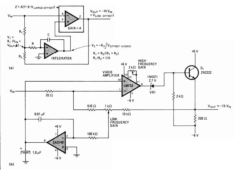
--------- Reducing offset. The offset voltage of a wideband video
amplifier can be reduced almost to zero if a resistor-scaled feedback
integrator is applied (a). Practical implementation (b) adds a zener
diode and an emitter follower in order to push the output of LM733, which
has a minimum positive output voltage, down to zero.
Dual-function amp chip simplifies many circuits
by Jim Williams National Semiconductor Corp., Santa Clara, Calif.
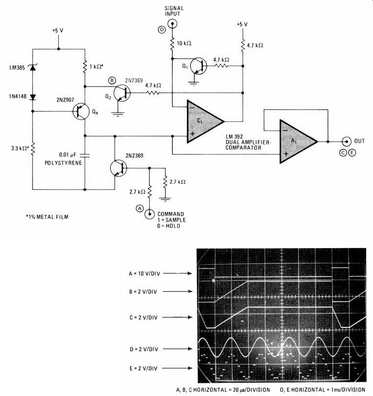
-------- 1. Compact sampler. A comparator and op amp chip consolidates
a sample-and-hold circuit, which utilizes only one supply, has virtually
zero gain error, and will not self-trigger. Owing to the configuration,
the device does not have to rely on the hold cycle, so that the circuit
is simplified.
Various circuits that combine low cost, single- or dual-supply operation, and ease of use can easily be built with comparators and operational amplifiers like National Semiconductor's LM339 and LM324 because of their general applicability to a wide range of design problems.
Now circuit complexity can be reduced even further with up-and-coming dual-function devices like the LM392, which put both a comparator and an op amp on one chip.
Besides allowing a degree of flexibility in circuit function not readily implemented with separate chips, this device retains simplicity at low cost. The building of such circuits as a sample-and-hold circuit, a feed-forward low-pass filter, and a linearized platinum thermometer is discussed here in the first of two articles.
The circuit in Fig. 1 is an unusual implementation of the sample-and-hold function. Although its input-to-output relationship is similar to standard configurations, its operating principle is different. Key advantages include no hold-step glitch, essentially zero gain error and operation from a single 5-volt supply.
When the sample-and-hold command pulse (trace A) is applied to transistor Q3, it turns on, causing Q4's collector to go to ground. Thus the output sits at ground.
When the command pulse drops to logic 0, however, Q4 drives a constant current into the 0.1-microfarad capacitor (trace B). At the instant the capacitor ramping voltage equals the signal input voltage, comparator C, switches, thereby causing transistor Q2 to turn off the current source. Thus the voltage at Q2's collector and A1's output (trace C) will equal the input.
Q1 ensures that the comparator will not self-trigger if the input voltage increases during a hold interval. If a dc-biased sine wave should be applied to the circuit (trace D), a sampled version of its contents will appear at the output (trace E). Note that the ramping action of the current source, Q4, will just be visible at the output during sample states.
In Fig. 2, the LM392 solves a problem common to filters used in multiplexed data-acquisition systems, that of acquiring a signal rapidly but providing a long filtering time constant. This characteristic is desirable in electronic scales where a stable reading of, for example, an infant's weight is desired despite the child's motion on the scale's platform.
When an input step (trace A) is applied, C1's negative input will immediately rise to a voltage determined by the setting of the 1-kilohm potentiometer. C1's positive input, meanwhile, is biased through the 100 K-0.01 F time constant, and phase lags the input. Under these conditions, C1's output will go low, turning on Q1.
This action causes the capacitor (trace B) to charge rapidly up to the input value. When the voltage across the capacitor equals the voltage at C1's positive input, C1's output will go high, turning off Q1. Now, the capacitor can only charge through the 100-W resistor and the time constant must therefore be long.
The point at which the filter switches from the short to the long time constant is adjustable with the potentiometer. Normally, this pot will be set so that switching occurs at 90% to 98% of the final value (note that the trip point is taken at about the 70% point in the photo so that circuit operation may be easily seen). A1 provides a buffered output. When the input returns to zero, the 1N933 diode (a low forward-drop type), provides rapid discharge for the capacitor.
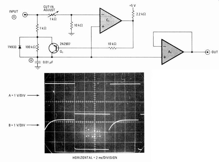
-------- 2. Feed-forward. This simple low-pass filter provides sharp
acquisition and long decay, so that it is perfect for multiplexed data
systems and electronic scales for infants. Its time constant is adjustable
with the potentiometer and is typically set to 90% to 98% of the full
input value.
In Fig. 3, the LM392 is used to provide gain and linearization for a platinum resistor-temperature device in a single-supply thermometer circuit. This one measures from 0°C to 500°C with ± 1° accuracy.
Q1 functions as a current source that is slaved to the 3.9-v reference. The constant-current-driven platinum sensor consequently yields a voltage drop that is proportional to its temperature. A1 amplifies the signal and provides the circuit output.
Normally, the slightly nonlinear response of the sensor would limit the circuit accuracy to about ± 3°C.
C1 compensates for this error by generating a breakpoint change in A1's gain at sensor outputs corresponding to temperatures exceeding 250°C. Then, the potential at the comparator's positive output exceeds the potential at the negative input and C1's output goes high. This turns on Q2, which shunts A1's 6.19-kQ feedback resistor and causes a change in gain that compensates for the sensor's slight loss of gain from 250° to 500°C. Current through the 220-kit resistor shifts the offset voltage of A1 so no discernible glitch will occur at the breakpoint.
A precision decade box should be used to calibrate this circuit. Once inserted in place of the sensor, it is adjusted for a value of 1,000 ohms and a 0.10-v output by means of resistor R1. Next, its resistance is set to 2,846 ohm (500°C) and its gain trim control adjusted for an output of 2.6 v. These adjustments are repeated until the zero and full-scale readings remain fixed at these points.
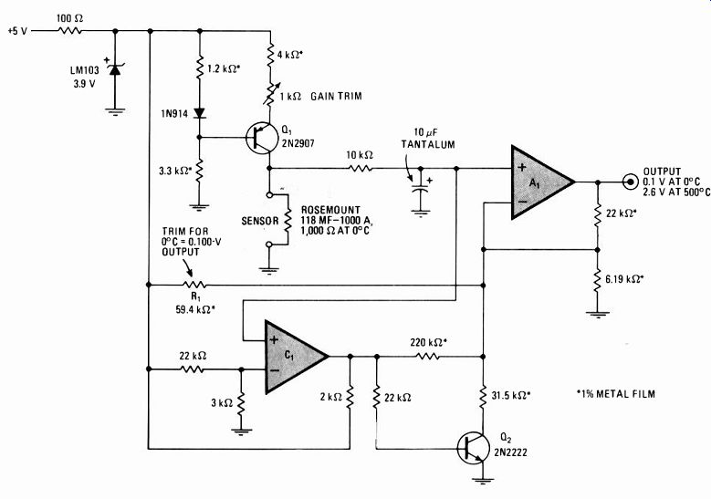
-------- 3. Tracking thermals. This platinum RTD thermometer has 99%
accuracy over the 0°-to-500°C range. C, derives the breakpoint change
in A1's gain for sensor outputs exceeding 250°C, compensating for the
sensor's nonlinearity. Current through the 220-kO resistor shifts the
offset voltage, in effect preventing glitches at the breakpoint. The
instrument is calibrated only at two points with a decade resistor box.
Dual-function amplifier eases circuit design
By Jim Williams National Semiconductor Corp., Santa Clara, Calif.
To simplify and cut the cost of the myriad of general purpose and specialized circuits, chips like National's LM392 combine both amplifier and comparator functions on a single substrate. As has already been noted [Electronics, May 5, p. 142], it can be used to build a sample-and-hold circuit, a feed-forward low-pass filter and a linearized-platinum-resistor thermometer. This article will present designs for its use in the construction of a variable-ratio digital divider, an exponential voltage-to-frequency converter for electronic music, and a temperature controller for quartz-crystal stabilization.
Figure 1 shows a divider whose digital-pulse input can be divided by any number from 1 to 100 by means of a single-knob control. This function is ideal for bench-type work where the ability to set the division ratio rapidly is advantageous.
----- 1. Analog digitizer. A single-control potentiometer sets the
digital signal's divider ratio from 1 to 100 using the LM392 comparator-amplifier
chip. Thus, the division ratio may be rapidly set. Staircase signals
are derived from a charge-balancing arrangement, which acts to maintain
Al's summing junction at a voltage null.
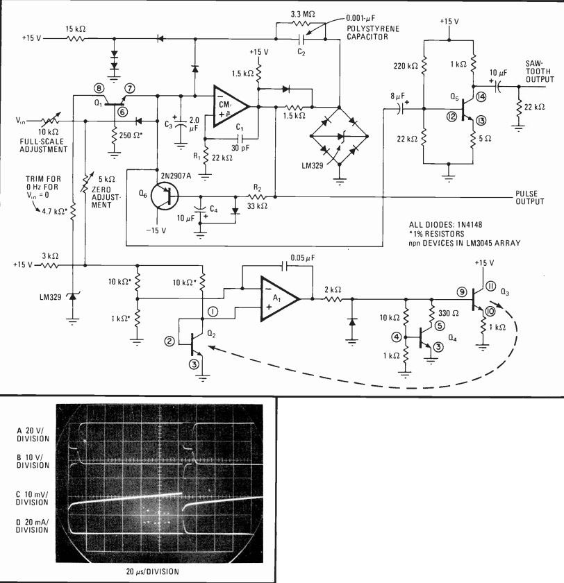
--------- 2. Sweet sawtooth. When combined with LM3045 transistor
array, LM392 forms the heart of an exponential function generator that
can easily be built. Waveform conformity to a pure exponential is excel
lent- ± 0.25% over the 20-Hz-to-15-kHz range. Thermal drift is minimized
with a simple servo loop. Provision is made for eliminating servo lock-up
under virtually all conditions.
With no input signal, transistors Q1 and Q3 are off and Q2 is on. Thus, the 100-picofarad capacitor (C1) at the junction of Q2 and Q3 accumulates a charge equal to Qcap = CiVo, where Vo is the potential across the LM385 zener diode (1.2 volts), minus the saturated collector-to-emitter potential across Q2.
When the input signal to the circuit goes high (see trace A, in the photograph), Q2 goes off and Q1 turns on Q3. As a result, the charge across C1 is displaced into A1's summing junction. A1 responds by jumping to the value required to maintain its summing junction at zero (trace B).
This sequence is repeated for every input pulse. During this time, A1's output will generate the staircase waveshape shown as the 0.02-microfarad feedback capacitor (C2) is pumped by the charge-dispensing action to the A1 summing junction. When A1's output is just great enough to bias the noninverting input of the comparator (CM) below ground, the output (trace C) goes low and resets A1 to zero. Positive feedback to the comparator (trace D) is applied through the 300-pF capacitor (C3), ensuring adequate reset time for A1.
Potentiometer R1 sets the number of steps in the ramp required to trip the comparator. Thus the circuit's input-to-output division ratio may be conveniently set.
Traces E through G expand the scope trace to show the dividing action in detail. When the input E goes high, charge is deposited into A1's summing junction F, and the resultant waveform G takes a step.
Professional-grade electronic-music synthesizers re quire voltage-controlled frequency generators whose output frequency is exponentially related to the input voltage. The one shown in Fig. 2 provides conformity within 0.25% over the range from 20 hertz to 15 kHz using a single LM392 and an LM3045 transistor array. These specifications will be adequate for all but the most demanding of applications.
------- 3. Oven cut. Quartz crystals are maintained at 75°C with
this temperature controller, thus stabilizing output frequency of these
sources.
Switched-mode servo loop simplifies circuitry considerably. Long-term temperature accuracy is estimated at 10 parts per million.
The exponential function is generated by Q1, whose collector current varies exponentially with its base-emitter voltage in accordance with the well-known relationship between that voltage and current in a bipolar transistor. An elaborate and expensive compensation scheme is usually required because the transistor's operating point varies widely with temperature. Here, Q2 and Q3, located in the array, serve as a heater-sensor pair for A,, which controls the temperature of Q2 by means of a simple servo loop. As a consequence, the LM3045 array maintains its constant temperature, eliminating thermal-drift problems in the operation of Q1. Q4 is a clamp, preventing the servo from locking up during circuit start-up.
In operation, Q1's current output is fed into the summing junction of a charge-dispensing current-to-frequency converter. The comparator's output state is used to switch the 0.001-uF capacitor between a reference voltage and the comparator's inverting input, the reference being furnished by the LM329.
The comparator drives the capacitor C1 and resistor R1 combination, this network providing regenerative feedback to reinforce the direction of its output. Thus, positive feedback ceases when the voltage across the RIC, combination decays, and any negative-going amplifier output will be followed by a single positive edge after the time constant R, C, (see waveforms A and B in the photograph).
The integrating capacitor C3 is never allowed to charge beyond 10 to 15 millivolts because it is constantly reset by charge dispensed from the switching of C2 (trace C). If the amplifier's output goes negative, C2 dumps a quantity of charge into C3, forcing it to a lower potential (trace D). When a short pulse is transferred through to the comparator's noninverting input, C2 is again able to charge and the cycle repeats. The rate at which this sequence occurs is directly related to the current into the comparator's summing junction from Q1. Because this current is exponentially related to the circuit's input voltage, the overall current-to-frequency transfer function is exponentially related to the input voltage.
Any condition that allows C3 to charge beyond 10 to 20 my will cause circuit lock-up. Q6 prevents this by pulling the inverting input of AI towards-15 v. The resistor and capacitor combination of R2 and C4 deter mines when the transistor comes on. When the circuit is running normally, Q6 is biased off and is in effect out of the circuit.
The circuit is calibrated by simply grounding the input and adjusting first the zeroing potentiometer until oscillations just start and then the full-scale potentiometer so that the circuit's frequency output exactly doubles for each volt of input (1 v per octave for musical purposes).
The comparator's output pulses while Q5 amplifies the summing junction ramp for a sawtooth output.
The circuit in Fig. 3 will maintain the temperature of a quartz-crystal oven at 75°C. Five-volt single-supply operation permits the circuit to be powered directly from TrL-type rails.
A1, operating at a gain of 100, determines the voltage difference between the temperature setpoint and the LM335 temperature sensor, which is located inside the oven. The temperature setpoint is established by the LM103 3.9-v reference and the 1-to-6.8-kilohm divider.
A1's output biases the comparator, which functions as a pulse-width modulator and biases Q1 to deliver switched-mode power to the heater. When power is applied, A1's output goes high, causing the comparator's output to saturate low. Q1 then comes on.
When the oven warms to the desired setpoint, A1's output falls and the comparator begins to pulse width-modulate the heater via the servo loop. In practice, the LM335 should be in good thermal contact with the heater to prevent oscillation in the servo loop.
Fm receiver mixes high gain with low power
by Peter Whatley Motorola Inc., Phoenix, Ariz.
Scanning receivers, ham transceivers, and other narrow-band frequency-modulated systems that receive voice or digital information need as much gain as they can get to pick up weak signals. Normally such gain is expensive.
But the Motorola MC3359P chip, which has an oscillator-mixer, limiting amplifier, quadrature discriminator, operational amplifier, squelch, scan control, automatic frequency control, and mute switch neatly combines low cost, high gain, and as a bonus, low power consumption.
It requires only a front-end tuner and a few other components to form a complete narrow-band scanning receiver (see figure).
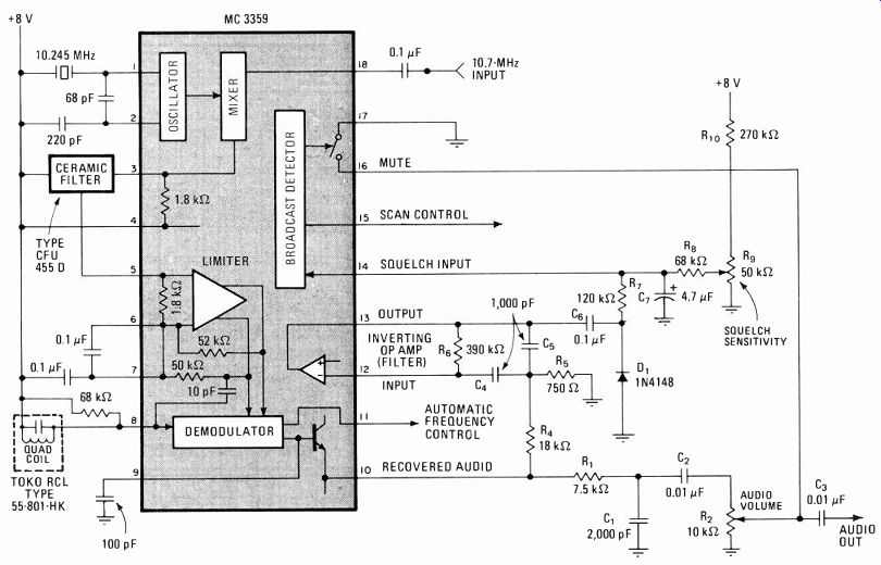
---------- Narrow band. In the scanning-receiver circuit shown, the
MC3359P provides an audio output voltage of 800mV peak to peak. Current
drain from a 6-V supply is 3 mA, and the sensitivity is 2µV for-3 dB
of input limiting. Only one crystal and some passive components are needed.
A typical application of the MC3359P is as a narrow-band fm scanning receiver for voice communication. As shown, the input to pin 18 (typically 10.7 megahertz) is converted down by a mixer-oscillator combination to 455 kilohertz, and most of the amplification is done by the chip at this frequency. The mixer is doubly balanced to reduce the fm receiver's spurious responses. Its output at pin 3 has a 1.8-kilohm impedance to match an external ceramic filter. For its part, the oscillator is a Colpitts design that can readily be controlled by a crystal.
After limiting, the fm signal is demodulated using a quadrature detector. The recovered audio is filtered through R1 and C1 to remove noise and is then coupled via C2 to a volume control. The recovered audio is 800 millivolts peak to peak at the junction of R2 and C2. The unfiltered recovered audio at pin 10 is fed through R4 to an internal inverting operational amplifier that, with R5, C4, C5, and R6, forms an active bandpass filter in the 6-kHz range. Therefore any noise or tone frequency, which may be present above the normal audio range, can be selected, amplified, and then detected by the C6 and DI combination. This detected signal is, in turn, sent to the squelch control at pin 14. Squelch sensitivity may be adjusted by R9, which provides a bias to the squelch input.
If pin 14 is raised to 0.7 volt by the detected noise, tone, or dc bias, the squelch detector will be activated.
This causes pin 15 to act as an open circuit and pin 16 to be shorted to ground via pin 17. Pin 16 is thus connected to the input of the audio amplifier and mutes the audio signal during squelching. Pin 15 can be used for scan control and may be connected to a frequency synthesizer in the receiver's front end. An afc connection is also available at pin 11. In this crystal-controlled application, an afc is not required, so that pin 11 can be grounded or tied to pin 9. With this last connection, the recovered audio is doubled in amplitude.
Agc prevents noise build-up in voice-operated mike by Russell S. Thynes Kirkland, Wash.
Hands-free operation of intercoms has several advantages over push-to-talk intercom systems. Constantly keyed "live" microphones, however, have the disadvantage of receiving undesirable environmental noise in the absence of speech. When such mikes are used in conjunction with intercoms having automatic gain control in the microphone mixing stages, this environmental noise will produce a swelling tide of sound each time normal communication is interrupted.
Shown here is an agc-vox (voice-operated switch) scheme that allows constantly keyed microphones to be used in noisy environments without suffering from the effects of noise build-up.
Although the operation of the circuit is twofold, the function is primarily that of a gain-clamped agc circuit.
Part (a) of the figure shows the transfer function of an agc with gain clamping and that of typical configuration. For input levels below those of normal speech, clamping the gain to a fixed value limits the area of the gain curve, reducing noise susceptibility-but without placing restrictions on the dynamic range of the agc itself.
The circuit is shown on the right (b). The agc section consists of operational amplifier A1 and transistor Q1, with diode D1 and capacitor C1 deriving the feedback control voltage. Q1 is placed in a T configuration to achieve a wide control range and to ensure low levels of distortion. Distortion is further reduced by the gate-biasing resistors R6 and R7. As configured, this agc should provide 30 decibels of gain control with less than 0.5% distortion for most of the audio range.
A3 is arranged as an adjustable noninverting amplifier, the gain of which can be varied from 20 to 40 dB.
R12 (also in a T configuration) allows the user to set the vox sensitivity to offset environmental noise conditions.
A4 simply compares the detected output of A3 with a reference and switches to either a high or a low output limit depending on the vox input level.
When input levels to the agc are below the vox sensitivity setting, the output of A4 will be at its lower limit, biasing Q1 off and thus clamping the gain of A1 to (R2+ R3)/R .
When the vox sensitivity level is exceeded, however, the comparator output swings to its upper limit and effectively disconnects the vox from the agc feedback loop through blocking diode D2. The gain is then expressed as:
(R2 + R3 R2R3 R2 + R3 <A < R1 R I Ro.R I )
where R.n is the practical on-resistance of the transistor.
This entire circuit can be configured using one quad op amp (such as an XR 4136) and requires no special considerations other than attention to the basic rules of grounding and supply bypassing.
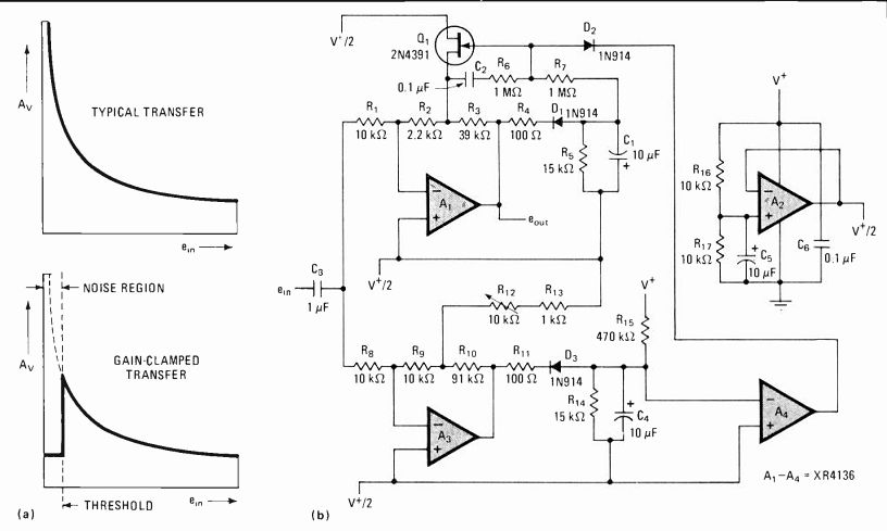
--- Hands off. If the gain is clamped to a minimum at input signal
levels below the noise threshold, the surrounding noise is filtered out
of the amplifier network (a), whereas speech kicks in the amplifier's
automatic gain control. Both functions are performed by the circuit shown
in (b).
Power-sharing bridge circuit improves amplifier efficiency
by Jim Edrington Texas Instruments Inc., Austin, Texas
This linear bridge amplifier offers several advantages in driving motors and servo systems, including obtaining maximum efficiency with a single power supply and with dc coupling, which as a result reduces circuit complexity.
Most notable, however, is that the four transistors in the amplifier will equally share load currents, as well as simplifying the drive requirements. These factors permit lower-cost transistors to be applied and allow their heat-sink requirements to be reduced.
Shown in (a) is one half of the bridge-type circuit, which illustrates the amplifier's operation. Positive input excursions from the driver turn on current sink Q2, with a portion of Q2's collector current passing through transistor Q3. Q3's current flow causes source transistor Q, to turn on.
Because the majority of the flow must pass through Q1 and Q2, the collector-to-emitter voltage of both transistors must be equal to ensure equal power dissipation.
This voltage-matching requirement is achieved by clamping the gain of Q1 to the voltage at the center of the load with a zener diode. Thus the virtual center of the load will be maintained at V./2 and VQ,c., = VQ,c, provided R1 = R2. The zener diode, 131, must have a value of Vz = (V./2)- 1.4 to meet the requirement for the reference potential.
Two of these circuits may be readily incorporated into a full-bridge arrangement, as shown in (b.), that is suit able for driving electromechanical devices. Adding diodes D2 through D5 isolate one branch's functions from the other. With this configuration, each branch conducts for half of the input cycle thereby eliminating virtually all crossover difficulties.
The isolation diodes will alter the divider's center voltage by 0.7 volts, however, and so the value of the zener voltage must be slightly changed. In this case, it will be Vz = (V./2)- 1.4 + 0.7 = 11.3 V. In most applications, selecting the nearest standard zener value will suffice.
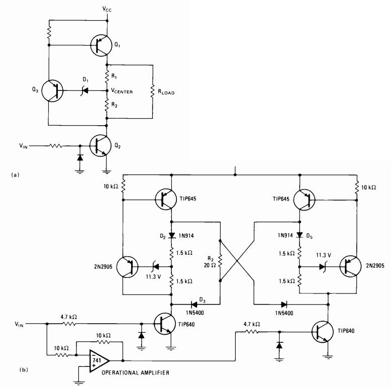
------------33 Divided driver. A rudimentary amplifier (a) may be designed
so that C1, and Q2 carry equal load on a positive excursion of an input
signal, using a zener diode of suitable value for biasing a load center
to cause Vo,c. = Vic.. Combining two such sections in a balanced bridge
arrangement (b) builds a dc-coupled amplifier that is simple, can run
from one supply, and can ensure that all amplifiers may handle a proportionate
share of the power. This combination reduces electrical specifications
of individual transistors, thereby reducing their cost.
Bi-FET op amps invade 741's general-purpose domain
by Jim Williams National Semiconductor Corp., Santa Clara, Calif.
Thanks to their low-drift microampere supply currents and pico-ampere bias currents, recently introduced bipolar field-effect-transistor operational amplifiers like National's LF441 can be used in applications that general-purpose amplifiers like the 741 cannot address.
A high-performance pH meter, logarithmic amplifiers, and a voltmeter-checker reference source may be inexpensively built with this bi-FET operational amplifier.
The low-bias input of the 441 provides an excellent non-loading port for a pH probe, which is used to measure the acidity or alkalinity of a solution (Fig. 1). This simple four-chip interface yields a linear 0-to-10-volt output corresponding directly to the value of the pH (0 to 10) being measured, a range that is more than adequate for many applications.
The output from buffer A1 is applied to A2, a tuned 60-hertz filter that removes power-line noise. A2 also biases op amp A3, which provides a compensation adjustment for the probe's temperature. A4 allows the probe to be calibrated.
To calibrate the circuit, the probe is immersed in a solution having a pH of 7. The solution's temperature is normalized for the meter by R1 , a 10-turn 1,000-ohm potentiometer whose value may be set between 0 and 100 units. These values correspond directly to a solution temperature range of 0° to 100°C. Potentiometer R2 is then adjusted for an output voltage of 7 v.
A conventional logarithmic amplifier (Fig. 2a) utilizes the well-known logarithmic relationship between the base-to-emitter voltage drop in a transistor and its co lector current. Here, AI acts as a clamp, forcing the current through Q1 to equal the input current, E./R,..
Q2 provides feedback to A2, forcing Q2's collector current to equal A2's input current, which is established by the LM185 zener-diode reference.
Because Q2's collector current is constant, its emitter-to-base voltage is fixed. The base-to-emitter drop of Q, , however, varies with the input current. The circuit's output voltage is therefore a function of the difference in the Vb, voltages of Q, and Q2 and is proportional to the logarithm of the input current. In this manner, the N7t, drift is cancelled. The coefficient of this term will vary with temperature, however, and cause a drift in the output voltage. The 1,000 ohm thermistor compensates for this drift, stabilizing A1's gain.
The 441's 50-pA bias current allows accurate logging down into the nano-ampere region. With the values shown in the circuit, the scale factor for the amplifier is 1 v/decade.
A second type of logarithmic amplifier is shown in (b).
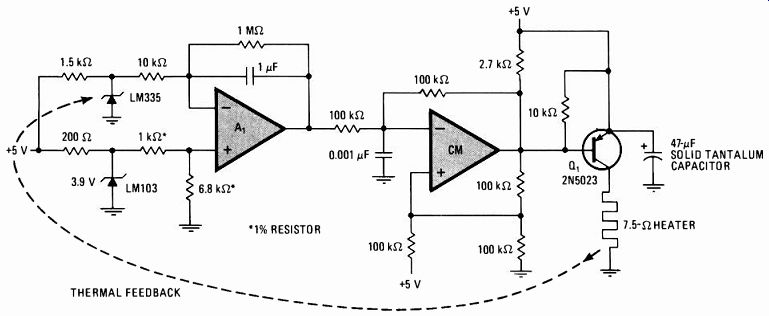
This unconventional design completely eliminates the temperature-compensation problems of (a) by temperature-stabilizing logging transistor Q1. This temperature problem is economically eliminated by utilizing the LM389 audio-amplifier-and-transistor array as an oven to control the logging transistor's environment.
Transistor Q2 in the LM389 serves as a heater, and Q3 functions as the chip's temperature sensor. The LM389 senses Q3's Vbe, which is temperature-dependent, and drives Q2 to feed back the chip's temperature to the set point established by the 1-to-10-kilohm divider. The LM329 reference ensures that the power supply is independent of temperature changes.
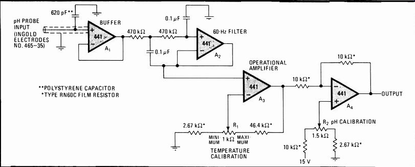
----------- 1. Acids and bases. This four-chip interface converts
the output of a pH probe into direct readings of a solution's acidity
and alkalinity. The circuit has a filter to reject the ac line noise
that plagues instruments of this type. This unit can easily compensate
for temperature variations.
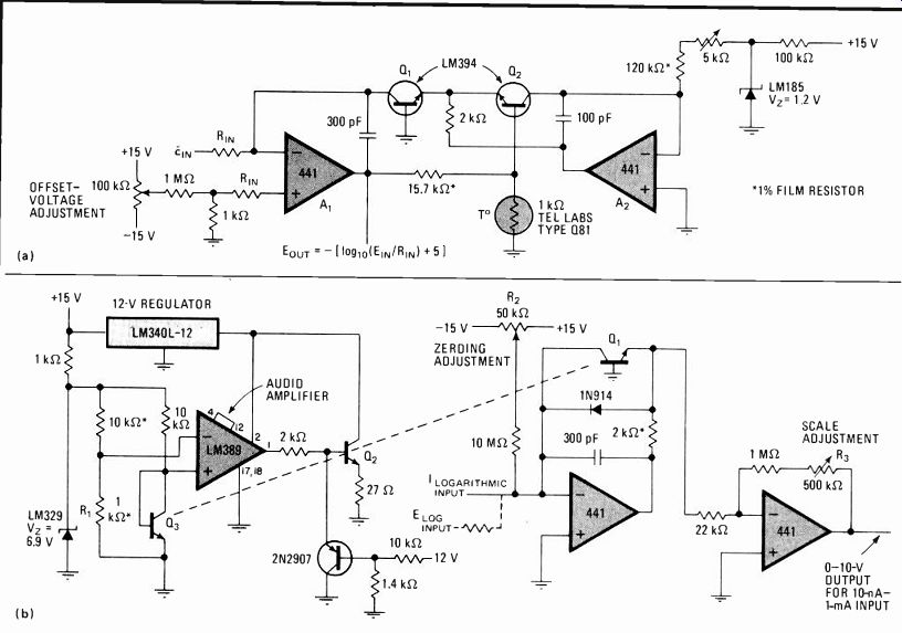
------ 2. Low-power loggers. With amplifier A, clamping current through
transistor (:), to input value En/FL, and with A2 holding Q2's current
constant with LM 185's reference, circuit (a) yields a logarithmic response
by virtue of proportional differences between Q1 and Q2's well-known
V_be-to-collector current relation. A more advanced version (b) uses
an LM389 to eliminate temperature effects on output.
--------- 3. Long-term accuracy. Using a single LF441 and a 1.2-volt
reference, this circuit for calibrating digital voltmeters with a 10-V
signal draws only 250 microamperes. Using a 15-v power source, the circuit
has an output accuracy within 0.1% over a year's time.
Q1 , the logging transistor, operates in this tightly controlled thermal environment. When the circuit is first turned on, Q2's current flow becomes 50 milliamperes forcing the transistor to dissipate about 0.5 watt, which raises the chip to its operating temperature rapidly. At this point, the thermal-feedback circuit takes control and adjusts the chip's power dissipation accordingly. The LM340L voltage regulator has only 3v across it, so it never dissipates more than about 0.3 w. The pnp transistor clamp at the base of Q2 prevents feedback lock-up during circuit start-up.
To adjust this circuit, the base of Q2 should be grounded, then the power applied to the circuit, and the collector voltage of Q3 measured at room temperature.
Next, Q3's potential at 50°C is calculated, a drop of-2.2 millivolts/°C being assumed. The value of R1 should be selected to yield a voltage close to the calculated potential at the LM389's negative input. After Q2's base is removed from ground, the circuit will be operational.
A1's low bias current allows values as low as 10 nano-amperes to be logged within 3%. Potentiometer R2 provides zeroing for the amplifier. Potentiometer R3 sets the overall gain of the circuit.
The low power consumption of the 441 is useful in a calibration checker for digital voltmeters that only draws 250 µA (Fig. 3). Here, the 441 is used as a noninverting amplifier. The LM385 is a low-power reference that provides 1.2 v to the input. This voltage is simply scaled by the feedback-resistor network to yield exactly 10 v at the circuit's output. The circuit will be accurate to within 0.1% for over a year, even with frequent use.
Current-biased transducer linearizes its response
by Jerald Graeme Burr-Brown Research Corp., Tucson, Ariz.
Transducers that work on the principle of variable resistance produce a nonlinear response when voltage-biased, as in common bridge configurations. However, a single operational amplifier configured to provide current biasing for the transducer eliminates this difficulty and allows output offset voltages to be controlled or removed.
As a voltage-biased transducer's resistance varies, so does the current through it. Thus, any signal voltage taken from the transducer will be a function of both current and voltage variations and will be a nonlinear function of the transducer's resistance.
Current biasing rather than voltage biasing avoids this nonlinearity, but reference current sources are not as readily available as voltage ones. Fortunately, an op amp can convert a reference voltage for this purpose and in addition provide other benefits.
In (a), a voltage-to-current converter circuit is adapted for voltage control of the supply current and of the output offset voltage. As laid out, the transducer's bias current is Ix = (V2-V 1)/R, , where V, and V2 are the externally applied control voltages. The current polarity can be set at either + or- , allowing an inverted or noninverted voltage response to variations in transducer resistance.
The resulting current flow in the nominal transducer resistance, R, produces an offset voltage at the circuit's output with a counteracting voltage developed by V,:
Vos. = (1 + (R2/R1))1sR-(R2/RO V1.
Thus, through the proper selection of V, , the output offset may be nulled to zero or set to either a positive or negative polarity.
Signal variations about that level result from a change in transducer resistance. The net voltage output then becomes eo = [1 + (R2/R1)146,R+ V.0. This response is linearly related to R. Also the signal is amplified.
To set the gain, R2 should be adjusted after R, , which sets the level of Ix, is selected. Because the output signal is taken directly from the amplifier's output, the transducer is buffered against loading effects.
Deviations in the described performance result primarily from voltage and resistor tolerances and from resistor-ratio error. Mismatch of the R2: R1 ratio is particularly serious, as this will make Ix somewhat a function of AR, thereby reintroducing nonlinearities in the circuit. Such a mismatch will alter the term in the denominator of the Ix formula to read ((R + AR)/R2) x ((R2/Ri)- (R2 /Ri' )), where R,' and R2' are the mismatched counterparts of R1 and R2, respectively.
Further errors will result from the dc input-error signals of the op amp. As a result, the deviation in e. will be:
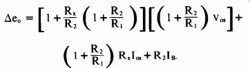
…where Vos, L, and IB are the input offset voltage, input offset current, and the inverting input-bias current of the op amp, respectively.
Making the R2/Rs ratio large reduces this error.
In practice, it is either inconvenient or sometimes undesirable to supply two voltage references to the circuit. A single reference voltage may be applied, as shown in (b), which is the Thevenin equivalent of the circuit in (a). For the specific component values given, the amplifier will deliver a 1.0-volt full-scale output signal with a zero offset in response to a transducer resistance that ranges from 300 to 350 ohms.
---------- Holding constant. A voltage-controlled current source
drives transducer (a) so that its output voltage is a function of its
resistance change only, thereby reducing the circuit's nonlinear response.
The output offset can also be virtually eliminated. The single-reference
current source circuit (b), which is the Thevenin equivalent of (a),
may be more attractive to implement in some cases.
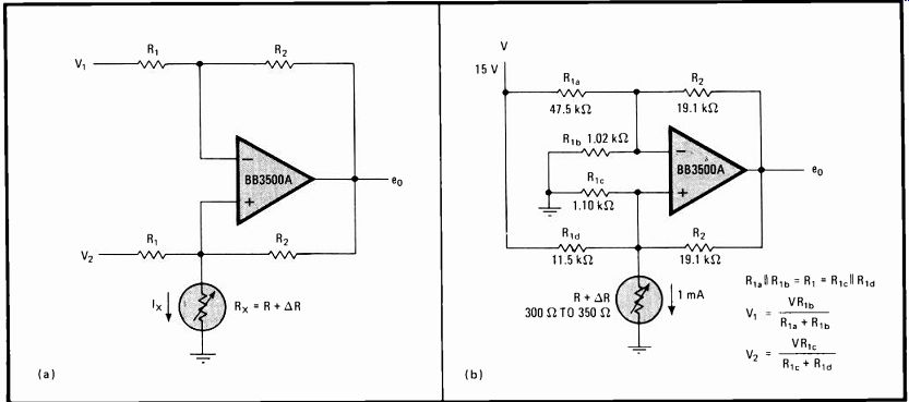
Counter indicates when its probe is compensated
by Dale Carlton Tektronix Inc., Beaverton, Ore.
Using a scope probe with a counter or other measuring instrument has a number of well-known benefits-namely, it ensures minimal source loading, physical ease of circuit connection, and minimum distortion of high-frequency signal components. Still, matching the probe to the counter's input impedance to secure wideband response can be troublesome, especially if the elements needed to perform the standard compensation procedure (a scope and a source of square waves) are not available and the input impedance of the scope and counter are not identical. Fortunately, the counter's own input-trigger circuit may be employed as a peak detector to indicate that proper probe compensation has been achieved.
The equivalent input circuit of the typical 5 x and 10 X (attenuating) probe appears as in (a), where C1 is the ac coupling capacitor and C2 represents the probe's compensating capacitance, cable capacitance, and the input capacitance of the measuring instrument. R, is the dc coupling resistance. R2 is the instrument's input resistance. For flat response, the product of R1 and C1 should to the product of R2 and C2.
Compensation is achieved by applying to the probe/counter a 1-kilohertz square-wave signal having a rise time of less than 100 microseconds. The amplitude of the square wave should be as large as the counter's dynamic range will allow. The counter should be set to trigger on the low-frequency components of the square wave so that a reference level is established. Then the probe's compensating capacitor is adjusted so that the counter will trigger on the highest-frequency components of the signal.
Specifically, the counter should be set to the 1X position. The counter's function control is then set to the frequency, period, or event position, so that the counter's display or input-trigger LED will indicate triggering when the square wave is applied.
To establish the reference level, the probe is adjusted so that triggering occurs in the waveform's so-called roll-off region. This is done by setting C2 and the trigger level in turn so that triggering occurs at the peak of the acquired signal and at the minimum level required to ensure consistent operation. The point at which this occurs for a given trigger level is reached when an increase or decrease in C2 does not stop triggering. If the acquired signal could be observed, it would appear as in the illustration in (b).
For compensation at the high frequencies, the response of the probe must be flattened (c). This is achieved by setting the trigger level to a position where triggering just stops or is erratic. C2 is then adjusted to the point where triggering is again reliable, and probe compensation is complete.
------------ Match. Universal counter's display or trigger LED is
used to indicate that probe/circuit's elements R1C1C2 (a) are matched
to input impedance (R2) of measuring device. Procedure used is to first
position triggering region on roll-off of input-signal curve (b) with
C2 and counters trigger-level control. Probe will be compensated over
a wide band after C2 is peaked (c) to detect high-frequency components
of square wave.
Availability of a constant-amplitude sine-wave oscillator greatly simplifies the compensation procedure.
Setting sine-wave frequency at 100 hertz and a convenient amplitude, the user need only set the counter's trigger level at the sine wave's peak voltage. The frequency is then increased to 10 kHz or higher and C2 is adjusted to just restore triggering. Typically, the flatness achieved by this method will be 2%. In equation form, %F = (AS)(100)/V1,,
where A is the probe's attenuation factor, S is the settability or trigger-level resolution, and V, ,p is the peak-to-peak amplitude of the input signal.
Some counters have a tapered trigger-level knob and the maximum setability occurs at the 0-volt level. For best accuracy when using one of these counters, a wave form that is square near 0 v or an offset sine wave that has peaks near 0 v should be used.
It should be noted that many of the newer counters now available have a large input capacitance, and some conventional scope probes may not have sufficient compensating capacitance. Using such a probe in this situation reduces system sensitivity above 1 kHz and could cause additional time-interval measurement error.
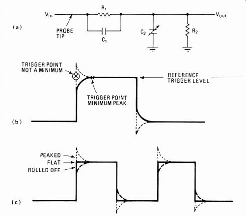
Transistor probe simplifies solid-state gaussmeter
by Shanker Lal Agrawal and Rama Swami Banaras Hindu University, Department of Physics, Varanasi, India
As a result of the subatomic energy exchanges that take place in many semiconductors because of particle-wave interaction, the electrical characteristics of the unijunction-transistor oscillator can be significantly changed by an external magnetic field. This property makes the low-cost unijunction transistor ideal for use as a probe in a gaussmeter or other flux-measuring instrument.
Although it is not as linear, is not as easily calibrated, and does not provide the readout precision of some of the more elegant designs,' this circuit is simpler, just as sensitive, and virtually as accurate.
--------- Flux finding. The low cost of the rudimentary unijunction
transistor, which is sensitive to externally applied magnetic fields,
makes it ideal for use In comparison-type gaussmeters. The circuit range
is 0 to 1.5 Wb/m^2, with circuit response linear to 1.0 Wb/m^2.
As shown, the gaussmeter is based on the comparator technique, wherein the frequency of the relaxation oscillator-probe is matched against a reference whose nominal frequency is about 400 hertz. Both generate positive-going spikes, which are lengthened by the pulse-stretching 74121 one-shot multivibrators. The NAND gate serves as a digital comparator, turning off the light-emitting diode when frequency f1 = f2.
In operation, the frequency of the reference oscillator is adjusted by resistor R until f2 equals the free-running (free-field) frequency of the probe. Placing the oscillator-probe within the field to be measured will cause its frequency to change; potentiometer R in the reference must then be adjusted until the difference between f1 and f2 is minimized. The change in resistance of R from its nominal position may then be related to the strength of the magnetic field with the aid of the unit's individual calibration curve, which is shown at the right side of the figure.
As for calibration, at least three standard magnets will be required over the range of 0 to 1.5 weber per square meter, which is the range of the instrument. The circuit response is not likely to be linear above 1.0 wb/m^2, and depending on the particular UJT used, the standard-marker points will vary considerably as a function of R.
Still, the circuit will hold calibration and will serve well in most general-purpose applications.
References
1. Henno Normet. "Hall-probe adapter converts DMM into gaussmeter," Electronics, Jan. 3, 1980 p. 179.
Five-chip meter measures Impedances ratiometrically
by N. E. Hadzidakis Athens, Greece
Measuring both inductance and capacitance usually requires either a manual bridge, which is difficult to use, or a digital bridge, which is expensive. Recently, inexpensive hand-held capacitance meters have appeared on the market, but they employ a time-to-charge technique that cannot be applied to the measurement of inductance. The circuit shown here, however, utilizes a ratio-metric method that is suitable for both types of measurement. Its only disadvantage is the requirement for one calibrated reference component per range. Still, it is inexpensive and easy to use.
Generally, the potentials across a reference and test inductor or capacitor, which are dependent on the frequency of the 8038 square-wave driving source, are applied to two ac-to-dc converters built around CA3130 operational amplifiers. The converters' output is then compared at the ICL7107 ratiometric converter.
Because the value of the reference inductor or capacitor is a multiple of 10, the value of the test element can be read directly from the display.
In the case of measuring inductors, it can easily be shown that:
Lx = L_ref /e 1,2ref e2(e + 1) / - 2 + 1/e 4- (2e + 1)- R2/4 pi^2 f^2
…where R is the dc resistance of L., f is the test frequency, and e is the display indication divided by 1,000 and with the decimal point disregarded. Because f is varied appropriately with range and the Q of Ler is greater than 100 at 1 kilohertz-coils are hand-wound on Amidon pot cores using the largest-diameter wire possible (see table)-the equation given above reduces to L. = Lrefe for almost all practical measurements. For example, the error in measuring a 1-millihenry inductor having a Q of only 0.1 at 1 kHz will be less than 1%.
The concept of measuring capacitance is similar.
Potentiometers RI, R2, and R3 are used to cancel out the effect of parasitic capacitance at the converter's input terminals so that the display will read zero with no test capacitor connected. When that is done, the display will read 1,000C./Cf.
Construction is not critical. The only exception to that is the wiring to the input terminals, which should be kept reasonably short.
The calibration procedure for the circuit is straightforward. S1 is set to 2 microfarads full scale and R1 is adjusted for a zero display reading. Then S1 is placed in the 20-nanofarad full-scale position and R2 adjusted for a zero reading. Finally, the switch is set in the 2-nF full-scale position and R3 adjusted for a zero display reading. In the prototype tested, no readjustment was necessary over a nine-month period of normal use, and accuracy was maintained to within 1%.
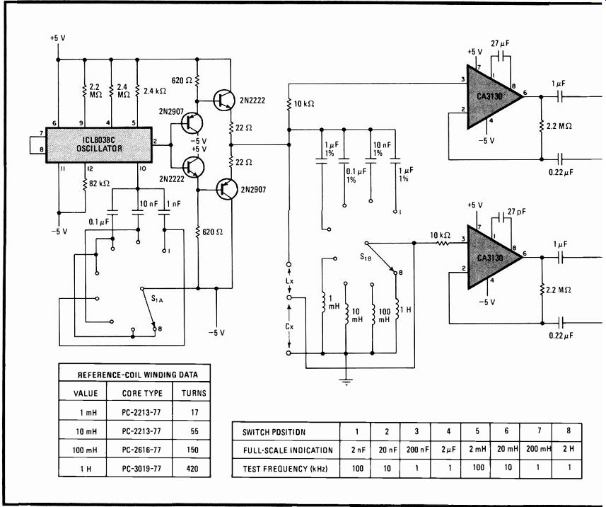
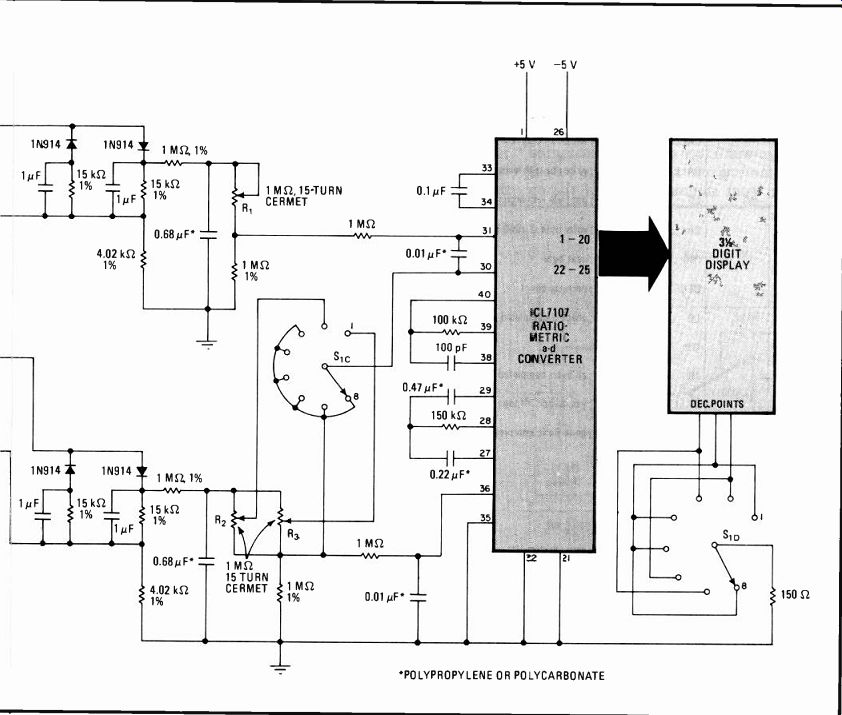
---------- Coils and capacitors. Ratiometric meter, easier to
use than manual bridges and less expensive than digital types, measures
inductances of reasonable Q over the 2-mH-to-2-H range and capacitances
over the 2-nF-to-2-AF range to within 1%. Calibration, required for capacitance
measurements, is easy and maintains long-term stability.
Charge-balancing modulator aids analog-signal isolation
by Tadeusz Goszczynski and Jerzy Harasimowicz Industrial Institute of Automation and Measurements, Warsaw, Poland
For engineers trying to solve ground loop problems in industrial instrumentation, here is a novel and inexpensive isolation circuit for analog signals. It employs a voltage-to-pulse-width modulator to convert analog signals into digital ones so that the job can be handled easily by low-cost opto-isolators. This is done by using a clock-synchronized charge-balancing scheme to economically achieve an accuracy of within 0.01%.
The charge-balancing modulator consists of an operational-amplifier integrator on the input that feeds the D input of a flip-flop. A constant-current sink and switch are driven by the flip-flop to produce a pulse whose width is proportional to the input voltage. This signal feeds the opto-isolator, the output of which is converted back into a voltage by the demodulator consisting of a synchronized flip-flop, a current sink, and an op-amp low-pass filter.
The voltage-to-pulse-width conversion is facilitated by switching the constant-current sink from the output of the flip-flop to the input summing mode of the op amp. Initially, the current switch is open, so that when the input voltage is applied, a negative-going ramp is produced at the integrator's output. When this voltage passes the flip-flop's input threshold voltage, it changes state synchronously with the next clock pulse, thereby closing the current switch. This action causes the reference current (which is always greater than the maximum input current) to be subtracted from the integrator's input current, producing a negative-going ramp at its output that eventually causes the flip-flop to toggle again. The time between toggles is proportional to the input voltage, and a transistor converts that time into a corresponding pulse width that drives the opto-isolator.
The current reference is actually a voltage-reference diode, D1, and a resistor, R1, that uses the fact that the integrator summing node is at virtual ground (0 volts) thus making the reference current equal to VREF/R 1.
Diode D3 compensates for temperature-caused variations in diode D2.
The demodulator relies on a synchronized flip-flop (driven from the same clock source) that can switch another current source on to charge capacitor C1 to the original input voltage. The active filter smoothes the demodulator's response.
The analog-signal isolator can handle signals between ± 10 v accurately to within 0.01% and has a frequency range of 0 (dc) to 100 hertz with a common-mode rejection of 100 decibels and an isolation of over 2,500 v dc between inputs and outputs.
---------1. Analog-signal isolator. Input voltages are converted
into proportional pulse widths that are fed to an inexpensive opto-isolator.
The pulse is then converted back into a voltage that tracks the input
voltage accurately to within 0.01%. The circuit uses a minimum of precision
parts.
[source: ISBN 0-07-606808-0 Copyright© 1982 by McGraw-Hill, Inc. ]