Two-chip radio link pilots toys and models
Transmitter and receiver ICs for multichannel remote control give low-cost digital and proportional system a 100-meter range
by Martin Giles, Kerry Lacanette. Dennis Monticelli, and Ron Page, National Semiconductor Corp., Santa Clara, Calif
Toys and model vehicles with radio-frequency remote control have long been limited to committed hobbyists and radio amateurs working with expensive control terminals. But the price of radio control will drop enough to spur a consumer boom now that inexpensive but sophisticated integrated circuits are moving into the field.
Penetration of this high-volume, low-cost market is helped considerably by ics designed for easy, reliable assembly and operation. Two of the first such chips, introduced at the end of 1978 and now in volume production, are the LM1871 encoder-transmitter and the LM1872 receiver-decoder. They make it possible to build a complete radio control system for only $10.
The LM1871 encoder-transmitter contains all the circuitry required to modulate an rf carrier as high in frequency as 80 megahertz with up to six analog channels of control information. The LM1872 receiver-decoder uses a combination of pulse-width and pulse-count techniques to recover two analog signals and to accommodate two others for digital (latched) service.
Alternatively, simple external circuitry provides for handling a total of four independent channels in any combi nation of analog or digital formats. The versatile chip pair thus may be adapted to many other tasks such as activating burglar alarms or the remote switching of lights, TV channels, or data links, to name just a few.
---------- REMOTE-CONTROL FREQUENCY ALLOCATIONS AND GENERAL REQUIREMENTS
---------- 1. Guidance. LM1871 encoder-transmitter guides toys and
models at 27, 49, and 72 MHz. Digital and proportional unit, shown configured
for two channels each of digital and analog data, can be set up to deliver
up to six channels of pulse-width-modulated information.
With or without a license
While sharing many of the features of the typical 0.75-watt, $200-to-$400 radio control set used by the serious hobbyist in the licensed portion of the spectrum at 72 MHz, the LM1871/LM1872 combination is also designed to provide superior performance over the frequencies where no operator license is required (see Table 1). The modulation technique used is compatible with the requirements of the Federal Communicationscom mission for all allocated frequencies. The decoding technique, suitable for use in the licensed bands at the allowed higher power levels, works equally well in the low-power unlicensed segments at 27 and 49 MHz.
The LM1871 is a six-channel combination digital and proportional type encoder and rf transmitter (Fig. 1). A bipolar linear device, it is designed to generate a field with a strength of 10,000 microvolts per meter at a distance of 3 meters from its antenna at frequencies up to 50 MHz. This is the maximum field strength permitted for unlicensed transmitters. Encoding involves a pulse width modulation scheme: analog information is converted into a train of pulses whose widths are proportion al to the corresponding channel inputs.
In practice, the analog information at each channel input, and thus the output pulse width, can be set by a potentiometer that corresponds to a given control vari able. Each of up to six pots may be sequentially switched to discharge the timing capacitor at pin 8, which is periodically charged by the 1871. The setting of switches A and B (pins 5 and 6) determines the number of channels sent in the transmitted pulse train. This number may vary from three to six. Each frame of six pulses lasts about 20 milliseconds, which includes a terminating sync pulse 5 ms long to allow the receiver to discriminate between one set of pulses and the next.
In operation, capacitor Cr at pin 8 is charged to two thirds of the supply voltage (KO through the pulse timer in a time determined by both RM and CT. This time corresponds to the carrier-off period. The capacitor is then discharged back down to one third of V. through external potentiometer Roil, which sets the carrier-on period for the corresponding channel, with the sum of the on and off periods constituting the pulse width for the channel. This width is usually between 1 and 2 ms, with a nominal 1.5-ms value. At the receiver, a corresponding potentiometer connected into a pulse recovery circuit is mechanically set in position by a servo, the servo rotating until the pulse widths at receiver and transmitter match.
Closed loop or open
This pulse-width matching is a form of closed-loop analog control: the rotation of the receiver's servo is proportional to the control position of the transmitter's potentiometer-that is, a steering, or positional function.
Alternatively, open-loop control can be obtained for any channel by omitting the corresponding receiver potentiometer and comparing the transmitted pulse with a fixed pulse width at the receiver (usually a 1.5-ms monostable vibrator triggered by the leading edge of the transmit pulse). A shorter transmitted pulse will cause the servo to rotate in one direction. Matching pulses will result in a stationary motor, and a wider transmitted pulse causes rotation in the other direction. The motor speed can either be fixed for positional control or variable, depending on the actual difference in the pulse widths for speed control. Because this open-loop method initially requires matched pulses for a stationary motor, the LM-1871/1872 can also use another method, described later, that avoids the need for a time reference to control latched channel controls (digital channels).
The typical transmitting antenna used in the field will be a telescoping or fixed wire antenna about 0.6 m in length. At 27 and 49 MHz, this length is less than one tenth of a carrier wavelength, so the antenna is capacitive. At 49 MHz, a 0.6-m, 5.6-mm-diameter antenna can be represented by a 6.2-picofarad capacitor. The ability of such an antenna to radiate power can be represented by an equivalent radiation resistance (RA) that would dissipate the same power. RA is given by:
RA = 40 (r L/X)2 ohms where L is the length of the antenna and X is the wavelength, both in meters. For an antenna 0.6 m long, RA equals 3.7812.
The current through RA needed to generate a given field strength, E (in µv/m), is given by:
IA = EdX/(1207L) where d is the distance in meters from the antenna.
Plugging in the FCC limit for E of 10,000 Av/m at d = 3 m, it is seen that the antenna current is 0.8 mA. If the capacitive reactance of the antenna is tuned out with a loading coil (resonating with 6 pF at 49 MHz) less than 3 my is required from the oscillator tank circuit, in theory.
The loss resistance, RL, is considerable, however, and must be taken into account. This resistance will be a function of the terrain, transmitter height, load mis match, and other factors. For a typical hand-held transmitter with a consequently poor ground return, RL will vary from several hundred ohms to kilohms. Practical tapped to deliver 20 my peak to peak at 49 MHz and about 200 my p-p at 27 MHz to the antenna loading coil in order for the 1871 to deliver the maximum field strength. The transmitter is regulated so that the maximum power output is maintained for a supply voltage variation extending from 16 down to 5 volts.
The extremely low radiated power permitted in the unlicensed bands does indicate one difficulty in utilizing these frequencies, apart from the limited range. Specifically, FCC regulations mandate that out-of-band emissions must be at least 26 dB below the peak permitted carrier level: that is, less than 500 µWm. Because of the substantial losses encountered in the antenna circuit, the oscillator power level must usually be made high to achieve the maximum permitted field strength. This means that the level of harmonics being radiated directly by the oscillator can easily be above the FCC limit if care in circuit layout is not exercised. Oscillator and output leads, including ground returns, should be kept as short as possible. Design and evaluation kits for both the 1871 and 1872 are now available for those who wish to eliminate construction-phase headaches.
Range versus terrain
The range to be expected with this low-power transmitter is dependent on the transmitting and receiving antenna heights and the local geography. Outdoors, the transmitted field strength can be expected to be similar to that of the color curves of Fig. 3, taken across an asphalt parking lot with a transmitter 3 feet above the ground. Wet grass or water and higher antenna locations will yield an increase in field strength for a given distance from the transmitter. In contrast, operation within buildings can drastically reduce range if they contain much metal. Metal furniture, refrigerators, filing cabinets or steel beams will cause dramatic local variations in field strength making any range predictions subject to large errors. However, in domestic environments, a range of at least 10 to 20 m can usually be attained.
But while the permissible output power is an important factor in determining the control range, of equal importance is the sensitivity of the LM1872 receiver.
Sensitive superhet
To obtain sensitivity along with good selectivity, the LM1872 (Fig. 2a) is configured as a single-conversion superheterodyne receiver. The local-oscillator and mixer stages are capable of operation up to 80 MHz with good conversion gain and low intrinsic noise. The intermediate frequency is 455 kHz, and a wide-range (97-dB) automatic-gain-control circuit is employed in the i-f amplifier to handle the wide range of input voltages typically encountered. This circuit also provides good immunity to voltage transients on the supply line. The active digital detector that follows raises the system gain to 88 dB. The resulting baseband signal is then applied to the decoding logic, so that the original signal information sent on each channel can be retrieved.
A high-gain precision comparator, a 30-As integrator, and a 25-mv reference make up the unique digital detector. When the signal voltage from the i-f amplifier exceeds 25 my (the detector threshold level), the comparator will drive transistor IQ" to discharge the envelope-detection capacitor, C12. A period of 30 As is normally required for the 1-AA current source to linearly charge C12 to the 3 v (V./2) level necessary to fire the Schmitt trigger. But the presence of the 455-kHz carrier waveform (2.2-As period) prevents C12 from reaching this threshold until the carrier signal goes to zero during the interchannel time. The Schmitt will respond 30 As later. This delay does not upset system sync since the LM1872 decoder responds only to the negative edges of the modulation envelope.
--- 2. Linkage. LM1872 (a) demodulates up to four channels of incoming
data, converting it into positional data for model vehicle's analog-
and digital-channel servos. Single-conversion superhet is built on par
with standard a-m receiver, except for digital decoder (b), which is
needed for extracting the timing and pulse-count data from carrier in
order to deliver the proper channel command to its corresponding servo.
--------- 3. Profile. The field transmitted by the 1871 (color curves)
induces a voltage at the 1872 receiver's antenna (black curve) sufficient
for operation at 100 m. The receiver's automatic-gain-control threshold
is reached at an input voltage of 250-280 µV.
Recovering the data
The decoder (Fig. 2b) extracts the timing information from the carrier for the analog channels (of which there are normally two) and the pulse-count information for the digital channels (normally two). At the heart of the decoder is a three-stage binary (flip-flop) counter, A-C, that is advanced by one count on each negative transition of the modulated carrier envelope.
When the rf carrier drops out for the first modulation pulse, its falling edge advances the counter. During this time the sync capacitor C6 is held low by transistor Q12.
When the carrier comes high again for the variable channel interval, C6 ramps toward V./2 through the 100-kO resistor but is unable to reach it in the short time that is available. At the end of the pulse, the carrier drops out and the counters advance once again. The sequence is repeated for the second analog channel.
Gates G1 and G2 decode the analog channels by examining the counter's binary output to identify the time slots that represent those channels. Decoded in this manner, the output pulse width equals the sum of the standard inter-pulse time and the variable pulse width representing channel information. A Darlington output driver then delivers the channel pulses to their corresponding servos.
Following the transmission of the second analog channel, one to four (in this case, two) pulses representing the digital information are received in the manner outlined in the detector discussion. Up until the end of the pulse group frame period, the decoder responds as if these pulses were analog channels, but it delivers no output. At the conclusion of the frame, the sync pulse is sent.
Because the sync time is always made longer than the period of the sync timer (pin 13), the timer can deliver a signal to monostable (one-shot) multivibrator A1. The first A1 enables gates G3-G6 to read the state of flip flops A and B into a pair of RS latches.
The latches can source or sink up to 100 mA, thus serving as an ideal device for transferring the digital command to its servo. If A or B, and thus its corresponding latch, is at logic 1, then its respective servo will be activated. Upon conclusion of the read pulse, one-shot A2 is triggered, the counter is reset, and the chain is ready for the next frame.
The motor noise factor The voltage induced by this encoder into a receiving antenna 0.6 m in length at 49 MHz is plotted in the solid black curve of Fig. 3. As seen, the maximum typical outdoor range will be 100 meters. The minimum receiver sensitivity needed to effect a successful command has been set at 15 Aiv nominal. Higher sensitivities can be easily achieved and the range possibly increased significantly, but the high-noise environment created by inexpensive servo motors themselves makes this consideration impractical for low-cost applications.
The automatic-gain-control (AGC) threshold is reached for an input of 250 to 280 Ay from the antenna.
This signal level corresponds to a position roughly 25 m distant from the transmitter. At the detector threshold level (12 dB below the AGC threshold), the antenna signal is 60 to 70 µ,v, corresponding to a minimum range between 50 m and 60 m. To run a small vehicle on a received signal of only 60 AV does require good suppression of motor noise. Although the LM1972 is immune to noise transients on the common supply lines, rf noise generated by the motor brushes will always be picked up at the antenna or i-f transformer windings. Motors with wire or carbon brushes are usually better in this respect than motors with metal-stamping brushes, but even the latter can usually be effectively suppressed by inductors mounted close to the brush leads. In applications where the drive or servo motors are more remote from the antenna circuit, the LM1872 can be designed with high er sensitivity. At the licensed frequencies around 72 MHz, the circuit is able to operate with a signal below 2 Ay at the antenna input.
Four-channel flight
The 72-MHz band is intended primarily for control of model aircraft, which often requires more than two analog channels. Expansion to four analog channels is easily accomplished by modifying the LM1871 encoding waveform such that channels 1, 2, 4, and 5 are pulse width-controlled by potentiometers. Channel 2 is made to emit a fixed long pulse (5 ms) such that after decoding channels 1 and 2 at pins 11 and 12, the LM1872 will recognize channel 3 as a sync pulse and reset the counter chain. Simultaneously, both digital channel outputs will be latched low and then channels 4 and 5 will be decoded at pins 11 and 12. Because the digital channels are at a logic 1 (high) during encoding of channels 1 and 2 but are at a logic 0 during encoding of channels 4 and 5, they can be used to steer the analog channels-providing four independent analog controls.
This type of transmitter encoding may also be used to provide simultaneous control of four independent single-channel receivers, each receiver using the digital channel output to identify its control pulse.
Other transmission media
Although the LM1871 and LM1872 have been designed primarily as an rf link, other alternatives are possible, including common carrier transmission, ultra sonic, or infrared data links. To use the LM1872 as an infrared receiver, the local oscillator is defeated and the mixer stage runs as a conventional 455-kHz amplifier.
For an ac line link, a 262-kHz i-f is more suitable but will have a similar configuration. The choice of carrier will depend largely on application-rf links being suited to relatively long-range outdoor mobile control, infrared and ultrasound to applications where room-limited trans mission is needed for privacy. Common carrier will apply best to stationary locations where communications is desired without additional wiring around a building.
Additional information is available in the application notes for the 1871 and 1872.
Transformerless inverter cuts photovoltaic system losses
Design eliminates the iron-core losses that hurt efficiency during long low-load periods
by Geert J. Naaijer Laboratoires d'Electronique et de Physique Appliquee, Limeil-Breyannes, France
The eventual viability of photovoltaic power systems for the home depends on more than the development of efficient solar cells. Any losses that can be eliminated from the system reduce solar-cell area requirements, making the system more competitive.
One place in the power system where significant losses occur is the dc-to-ac inverter. Iron-core losses in a typi cal inverter's transformer can impair a solar power system's efficiency during the long off-peak hours of a daily load cycle. Thus a transformerless inverter design was developed to boost the efficiency of a photovoltaic system and reduce its solar-cell area requirements substantially [Electronics, Dec. 6, 1979, p. 69].
The 2-kilovolt-ampere prototype stepped-sine-wave inverter described here is the result of approaching the classic problem of dc-to-ac conversion in a new way. A 2-kvA production version will be marketed this fall by OMERA (Societe d'Optique, de Mecanique, d'Electricite et de Radio) in Argenteuil, France, a subsidiary of NV Philips Gloeilampenfabrieken (as are the Laboratories d'Electronique et de Physique Appliquee).
This design yields a conversion efficiency that is high on the average because its no-load losses are low. The following example demonstrates the importance of reducing no-load losses in a photovoltaic system.
----------- 1. Diode protection.
Stacked arrays of photo cells require protective di odes if the array is large.
Parallel diodes across series cells prevent excessive power dissipation should the accumulated voltage reverse-bias a weak cell.
Series diodes between parallel arrays further isolate the branches and reduce the chance of damage.
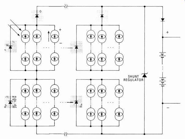
------------- 2. Switched on. Eight separate battery modules are switched
onto the bridge circuit in a sequence dictated by the control electronics.
Output voltage is determined by the number of modules on line; the bridge section adds polarity reversals. Part numbers are European.
A solar-powered house
It is reasonable to assume that with thermal collectors providing central heating and hot water, a family of four could live comfortably using about 10 kilowatt-hours of electrical energy per day. This example also assumes a sunny climate such as that in the south of France, a 5-kilowatt peak photovoltaic array, and 200 kwh of backup battery storage.
If inverter losses are considered negligible, 70 square meters (84 square yards) of silicon photovoltaic panel are required. A typical commercial photocell module measures 38 by 102 centimeters (15 by 40 inches) and generates 33 watts peak at about 16 volts. Each module contains 36 monocrystalline silicon cells in a clear silicone resin sandwiched between two glass plates.
The 5 kw required would be produced by 150 such panels. The array of cells would constitute a major part of the system cost. Yet by using an off-the-shelf inverter with a 90% full-load efficiency, photovoltaic array requirements would double.
The reason is that in this application, the inverter will operate, on the average, at a power level less than one-tenth of what it is rated to handle. This is similar to the situation faced by the utility companies, which must meet peak power demands and then run their generators underutilized for a large portion of time. As a result the no-load, or fixed, losses of the inverter become an important factor in determining the overall system efficiency, and hence the cost. For example a 10-kwh daily demand, an average demand of only 417 watts, would nevertheless require a 7.5-kw inverter-large enough to handle the possible simultaneous load demands from a washing machine and other heavy equipment. In fact, the inverter would need to withstand occasional transient demands as high as 10 kvA.
To determine the losses, recall that efficiency, n, is given as:
= Pout/Pm = PO ,/(Pout + losses)
where P, and Pci, are input and output power, respectively. If n is 90% and P0,, is taken as 7.5 kw, losses work out to 833.3 w, or 11.1% of the nominal output. Assuming for the example that fixed losses and proportional losses are equal at full load, then each constitutes 5.5% additional input power required, and the total input energy required to supply the 10-kwh demand can be derived.
Continuous 24-hour operation of the inverter is also assumed, so the daily fixed losses are 24 hours x 417 w, or about 10 kwh, and daily proportional losses are
0.055 x 10 kwh = 0.550 kwh.
The total daily input energy to supply a 10-kwh demand is then 20.55 kwh, and overall system efficiency is therefore about 50%. Furthermore, demanding only 10 kwh from an inverter that is designed to supply 180 kwh per day is wasteful. The total energy could be supplied only by increasing the number of photovoltaic panels from 150 to 300, doubling the investment in arrays of photovoltaic cells.
No-load losses
The major contributors to no-load losses in power inverters are transformer magnetizing currents, hysteresis, and eddy currents. In contrast, proportional losses are due to semiconductor voltage drops, switching losses, and IR drops and have relatively little impact on overall system efficiency; for practical purposes they can be neglected. The key to efficient low-power inverter operation rests, therefore, in the reduction of iron losses.
Before abandoning the transformer-based power inverter, however, several solutions that do use the device should be considered, since the inherent limitations of these alternatives are the stepped-sine-wave inverter's justification in the first place.
To sidestep the imposing fixed losses of conventional ac power inverters for widely varying loads, a system designer could:
Automatically cut off the inverter when there is no electrical demand.
Provide two or more inverters of different rated power, for example, 4, 2, and 1 kvA, and provide an automatic circuit for selecting the most appropriate combination at any given time.
Assign a high-power inverter for high-demand equipment and a smaller one to low-demand appliances.
Impose a particular time schedule on the use of various equipment in order to have the inverter always operating near its optimum working point.
Assign an inverter to each piece of equipment.
Install a mixed ac and dc electrical distribution net work, using dc wherever possible.
Each of these alternatives adds expense, and some are not very effective. It is clear that with a transformerless inverter design it would be possible to obtain much higher efficiencies, especially at output power levels well under the rated maximum.
The stepped-sine-wave inverter differs from more common designs not only, by eliminating the power transformer. It also exploits a feature peculiar to photo voltaic power plants, that of modularity.
The stepped-sine-wave inverter develops an ac output from an array of dc sources, in this case batteries, photocells, or both. The output voltage is varied by rapidly changing the connections between each source in the array into different series and parallel circuits. The output is stepped higher and lower, positive and negative as the interconnecting switches rearrange the connections between sources.
Actually the output is not a pure sine wave, but a staircase function simulating a sine wave. By smoothing the edges of the staircase with filters and providing a sufficient number of steps, a sine wave, for all practical purposes, is produced.
Multiple dc inputs
Unlike conventional transformer-equipped inverters with two input lines to accept dc and two output lines supplying single-phase ac, the stepped-sine-wave device accepts a multisource, reconfigurable arrangement at its input. This is what most photovoltaic power plants with stacked solar panels look like.
There are limitations on the stacking of photovoltaic panels beyond which protective measures should be taken. Protective diodes must be strategically placed in series and parallel, as shown in Fig. 1, to prevent damage and breakdown.
Parallel diodes are placed across series-connected photocell branches because, as the total series voltage accumulates in the string, single cells may become reverse-biased, causing excessive local power dissipation. Also, in parallel-connected photocell branches, sometimes one or more branches become a load for the others, again dissipating excessive power. This is prevented by isolating the interconnected solar panels with series diodes.
Typically, the unprotected array is safe for up to 10 branches connected in parallel, with each branch at a nominal voltage of 48 v for battery loads. If a higher voltage is desired, subassemblies of photocells or batteries may be connected in series. For example, 10 36-v assemblies connected in series are sufficient to drive the input of a transformerless power inverter capable of delivering 220 v ac.
Rapid electronic commutation of voltage sources is the basis of the stepped-sine-wave inverter. However, even relatively slow, time-dependent commutation of array interconnections can prove very useful. Being able to modify the interconnection of separate arrays allows the system to adapt to changes in photocell output.
Consider as an example the application of six photo cell subassemblies to the task of charging a battery. Two parallel rows of three subassemblies each would be con figured in series at high light levels and reconfigured as three parallel rows of two for low light levels. Note that judiciously adding steering diodes to the network reduces the complexity of the array wiring.
Another case of stepwise commutation of a photocell array is one where its output is defined over a period of one day. The array might be used, for example, to match the output variations of a non-tracking photocell array to loads such as pumping and irrigation systems where it is preferable not to use batteries. If, for instance, the pump is a lift type with a constant torque and the motor a dc type with a permanent magnet needing constant-current drive, a commutation scheme could be used to give near-constant current at optimum power output while the available light impinging on the cells goes through daily half-wave sinusoidal variations. In this case, the output voltage of the photocell array will show daily variations very close to a half-wave-rectified sine wave.
The concept of varying the wiring configuration of individual voltage sources is the principle behind the stepped-sine-wave inverter. By speeding up the commutation and using semiconductor switches, any waveform can be synthesized, including a 60-hertz sine wave.
Power circuit Figure 2 illustrates the power section of the inverter.
The contents of a read-only memory within the control electronics defines the position of the solid-state switches. This memory is addressed by a clock-driven counter. The switch positions are changed rapidly, connecting the photocell/battery modules to produce the stepped 60-Hz output.
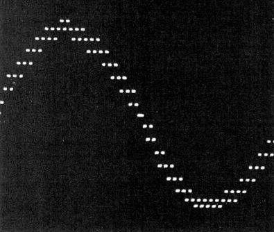
---- 3. Many possibilities. A hybrid waveform incorporating staircase
and pulse-width modulation is one of an infinite variety of simulated
waveforms possible with the stepped-output inverter. The 50-hertz wave
shown has peak-to-peak voltage of about 700 volts.
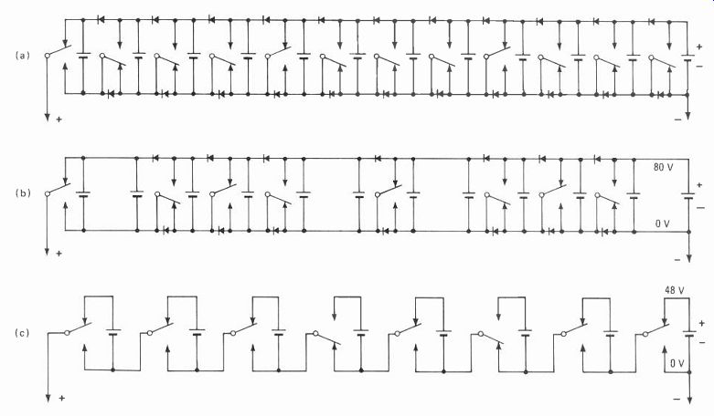
---------- 4. Commutation schemes. The general form for wiring sources
(a) can be simplified, giving fewer combinations of series and parallel
connections (b) but retaining equal discharge rate for each source. Further
simplification is possible (c), but the equal discharge rate is lost.
-------- 5. Polarity reversal. Bridge circuit operation is depicted
here by the load switches (tinted), which alternate to produce the positive
and negative excursions of the sine wave. In the actual circuit, optically
coupled silicon switches are driven by the control circuit.
The ROM stores the code for many cycles of the sine wave. In this way, the source commutation can be varied to guarantee equal average discharge of the batteries.
The zener diodes protect the batteries from being over charged, the bypass capacitors isolate the photocells from high frequencies, and a low-pass filter reduces the radio-frequency content introduced by the switching.
Figure 3 depicts the waveform obtainable with this circuit. The total harmonic content is slightly over 5%.
Regulation of the voltage is desirable not only from the standpoint of a changing load, but also because of the variations in battery voltage, which can swing from 20% above to 10% below its nominal value.
One way to achieve regulation is to modulate the commutation angles, which will increase slightly the total harmonic distortion. Another way is to pulse-width- modulate the voltage steps so that particular steps dwell around the ideal sine curve. Both methods require some feedback arrangement, but it need not be complex.
In comparison with conventional PWM switched-mode power supplies, transient amplitude and commutation frequencies are lower. These lower frequencies ease the tasks of filtering and of reducing iron losses in the filters.
The basic operation of the inverter in Fig. 2 can be understood by considering Fig. 4a. A multiple-source arrangement is shown wherein each battery connects to a single-pole, double-throw switch and is coupled to adjacent batteries by diodes.
Flexible switching A special simplified case of this general structure was described in the example of the commutated photocells, using sub-arrays with values that are not necessarily equal and with fewer, simpler switches. With 12 identical 80-v batteries, the circuit in Fig. 4b allows six different output voltages through the use of appropriate switching combinations, namely, 0, 80, 160, 240, 320, and 480 V. In the configuration shown, batteries are discharged at an equal rate, obviating the need to keep track of different levels of charge in each battery. Other configurations may result in unequal discharge rates. However, since the circuit is reconfigurable, periodic changes can be made to balance the overall discharging of each battery.
The point is that there are numerous ways to configure an array of voltage sources to make stepped changes in output voltage. In fact, almost any waveform can be generated. It is this concept of time-dependent commutation from which the design of the stepped-sine-wave inverter is drawn.
The circuit of Fig. 4c omits all diodes and uses eight identical 48-v batteries. This allows output steps of n x 48 v, where n = 0, 1, 2, 3, . . . 8, and is the circuit on which the 2-kvA prototype stepped-sine-wave inverter is based. Cyclic commutation of the batteries ensures equal average discharge of all batteries. Going one step fur ther, it is possible to monitor the batteries and electroni cally reconfigure them according to need or to isolate bad cells entirely from the system.
But these circuits simulate only positive- or negative-going waves, not both. To simulate a full sine wave, the voltage output must go positive and negative, and this can be accomplished in at least two ways. A complete sine wave may be synthesized using two sets of batteries and switches, so that positive and negative battery assemblies are switched at 60 Hz. Alternatively, a single bank of batteries and switches can be switched by an electronically controlled full-wave bridge circuit (Fig. 5).
The latter technique was selected for the prototype.
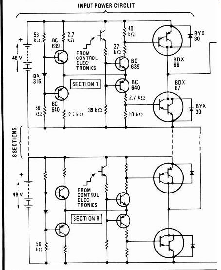
Isolation between the prototype inverter's control elec tronics and its power circuitry is achieved with optical couplers (Fig. 6). The power switch associated with each battery consists of complementary Darlington power switches shunted by power diodes that bypass inductive spikes. The bridge that performs the polarity reversals has four identical power Darlington transistors, each shunted by power diodes. All power for the switching and bridge circuitry is drawn directly from the source voltage, and no auxiliary power supplies are needed.
Feedback resistors sense the output voltage and current. This information is compared with the reference signal generated in the control electronics and is used for error correction in the power switches.
The control electronics are very simple and contain less than 10 common integrated circuits such as LM339 quad comparators, LM324 quad operational amplifiers, complementary-Mos gates, one-shots, an up-down counter, and a 32-byte ROM controlling the optical cou plers. The clock frequency applied to the counter is on the order of several kilohertz. The counter's output addresses the ROM, whose output controls the optical couplers and therefore drives the power circuitry that determines the output voltage.
Comparison of the actual inverter output voltage with the reference sine wave generates a control signal that determines the operating mode of the up-down counter.
The up-down counter is also controlled by feedback from the output current of the inverter. If the current exceeds a preset threshold, the counter is made to decrement rapidly, bringing the output voltage to zero. Regulation is excellent and the waveform is clean enough to run a color television receiver.
Efficiency is also excellent. At full load, it exceeds 93%®. At a 100-vA output, 5% of rated output, efficiency still exceeds 90%. No-load power consumption is just 5 w and would not be much higher for a similar 10-kvA design. Total harmonic distortion is under 15%, typically 12% without any filtering.
-----------6. In control. The power circuit receives switching commands
from a read-only memory coded for the desired waveform. Polarity reversals
are triggered by a reference sine-wave generator but may also be in ROM.
Voltage- and current-sensing taps guard the output limits.
-------- 7. Tapping Sol. If the battery modules are separated into
two blocks, one may be charged by photovoltaiccells while the other powers
the inverter load. The two halves exchange roles when a block approaches
either an upper limit of charge or a lower limit of discharge.
Potential for photovoltaics
In a system for providing sun-generated electricity, the dc photocell array and ac inverter output can be isolated by splitting the battery assembly into identical halves, each capable of supplying power for prolonged sunless periods. As one half is charged by the photocells, the other is connected to the load via the inverter. When either bank is close to its upper limit of charge or to its lower limit of discharge, the halves are switched. Auto matic commutation can be performed at night during low-load conditions by a motor-driven contact assembly.
Such a twofold battery arrangement (Fig. 7) simplifies battery inspection, maintenance, and replacement.
Since each half will have several days' capacity, daily commutation will ensure practically identical states of charge for the two banks, and sufficient reserve capacity is available to bridge maintenance periods. As batteries are kept at nominal voltage levels (between 1.85 and 2.05 v per cell), regulation is held within ± 5% without additional feedback circuitry.
If necessary the inverter can also operate as a battery charger supplying power from the main power lines.
Additional flexibility and built-in functions may be implemented by replacing the ROM in the inverter with a microprocessor.
++++++++++++++++++++++
Achieving stability in IC oscillators
Waveform-generator chips that operate above 1 megahertz rely on emitter-coupled circuits needing sophisticated temperature compensation
by Ilhan Refioglu, Exar Integrated Systems Inc., Sunnyvale, Calif.
Monolithic waveform and function generators form the backbone of circuits in a wide range of applica tions- telecommunications, data transmission, and test-equipment design and calibration. These integrated-circuit oscillators are characterized by an output wave form that is well-defined, repeatable, and stable despite changes in ambient temperature and power-supply level.
Modern waveform- and function-generator ics are overcoming the limitations of older IC oscillators like phase-locked loops and voltage-to-frequency converters.
The latter type of device is limited in performance by the fact that it provides only pulse-train or square-wave outputs. Waveform and function-generator chips, on the other hand, provide a wider variety of output waveforms, A function-generator ic generally consists of a current- or voltage-controlled oscillator section that gener ates the periodic waveform and allows for frequency variation, a wave-shaping section-basically, a sine-wave shaper-and a modulator (Fig. 1).
The heart of any function-generator IC is the oscillator section. This circuit determines the chip's most impor tant performance characteristics. These include stability with power-supply voltage and temperature changes, frequency range, sweep linearity, and so on.
There are two major types of IC oscillators, differenti ated mainly by their ability or inability to operate at frequencies above 1 megahertz. Oscillators that operate under 1 MHz generally employ lateral pnp transistors for switching and saturated logic. Their operating frequen cies are limited in practice to several hundred kilohertz.
But they also feature high stabilities of 50 parts per million per °C or less, thanks to careful compensation techniques employed in their designs.
-----------1. Functions. Generating waveform functions involves three
major circuit elements: a basic oscillator to produce a periodic and
variable-frequency wave, a wave-shaping section, and a modulator. The
oscillator frequency is controlled by either a voltage or a current.
--------- 2. Stable. A basic RC multivibrator oscillator (a) offers
high stabilities, but its lateral pnp transistors limit it in operating
frequency to about 100 kilohertz. An implementation similar in concept
(b) differs in that two current sources, I, and 12, are used in place
of resistors R, and R2.
Speed versus stability
Oscillators that operate above 1 MHz employ emitter-coupled multivibrators and npn transistors. They are inherently capable of operation up to 10 MHz. But they also suffer from frequency instabilities of more than 150 ppm/°C and low-frequency inaccuracy.
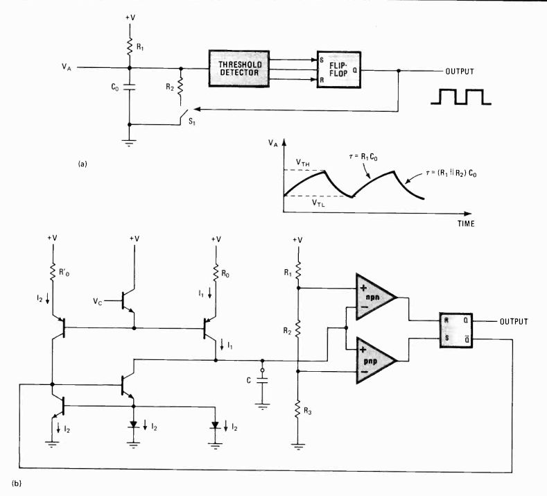
Figure 2a shows a basic RC multivibrator low-frequency oscillator circuit that has gained wide accept ance among lc oscillator designers. Capacitor Co is exponentially charged through resistor R1 to the supply-voltage level. When the voltage across Co ramps up to the higher of two threshold values, VTH, the threshold detector changes the flip-flop's state, thus closing switch Si (usually a transistor). With SI closed, Co starts discharging its voltage exponentially to ground through the parallel combination of R1 and R2. When Co's voltage reaches a lower threshold, VTL, the threshold detec tor is once again activated, causing the flip-flop to revert to its original state, and the charging process is repeated.
Note that if R1 is small, an exponential sawtooth wave form is obtained. If R2 is much larger than RI, the output waveform will be symmetrical.
A circuit similar in principle to that of Fig. 2a uses two current sources, II and 12, in place of R1 and R2 to generate a linear ramp waveform across the capacitor.
When current 12 is equal to 2I1, a symmetrical-output triangular or square waveform is obtained. A practical implementation of this circuit is shown in Fig. 2b. This type of circuit is employed in the ICM803 8 lc oscillator from Intersil Inc., Cupertino, Calif. Charging and dis charging of capacitor C are performed by currents II and 12. II and 12 are equal to the supply voltage minus Vc divided by resistors Ro and RO, respectively. Although II is always on, 12, which is doubled by the current mirrors, is switched on and off by the flip-flop's output. II performs the charging function while current 212- 11 does the discharging.
------------- 3. Voltage-controlled. This voltage-controlled oscillator
is used in the popular 565 phase-locked-loop integrated circuit and in
a function-generator IC, Signetics' NE566. Another astable multivibrator,
it uses one voltage-controlled current, lo, to charge and discharge capacitor
C_o.
If resistors Ro and RO are equal, then II equals 12 and C is charged and discharged by identical currents, leading to symmetrical output waveforms. Oscillator frequency for this case is a constant value, k, multiplied by I1C. Since current is set up by a control voltage, this circuit is known as a voltage-controlled oscillator.
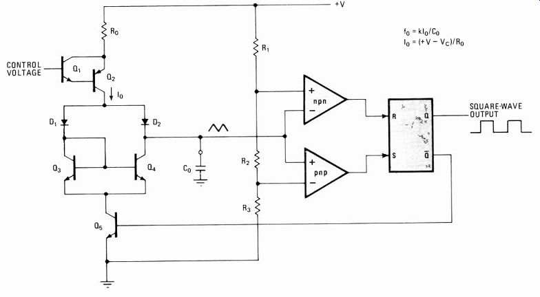
A different type of vco circuit is the one used in the popular type NE566 function-generator is from Signe tics Corp., Sunnyvale, Calif., and others. It is also used as the vco for the Signetics 565 phase-locked loop IC.
The circuit and its implementation are shown in Fig. 3.
The same voltage-controlled current, 10, is used to charge and discharge capacitor Co via the actions of the flip-flop circuit.
When transistor Q5 is off, Io charges Co through diode D2. When the voltage across Co reaches the trip point of the comparator, the flip-flop changes state and Q5 is turned on. At this point D2 becomes back-biased and Co is discharged through Q4 by the mirrored current, Io, until the voltage across Co reaches the lower threshold level. Then the flip-flop reverts to its original state, turning off Qs and repeating the charge-discharge cycle.
Since the same current is used for charging and dis charging, the circuit's duty cycle cannot be varied.
The oscillators of Figs. 2 and 3 are astable multivibra tor circuits. They exhibit good stabilities, in the range of 50 to 100 ppm/°C. Unfortunately, they are limited to a maximum frequency of about 100 kHz due to the use of lateral pnp transistors.
Emitter coupling for higher frequency Figure 4a shows a simplified schematic of an emitter-coupled multivibrator oscillator capable of 20-MHz oper ation. This circuit is difficult to compensate for changes in temperature, however, for very good frequency stabili ty at high operating frequencies.
Transistors Q1 and Q2, resistors RL1 and RL2, and the timing capacitor C form the heart of the multivibrator.
The clamping action of D1 and D2 and the level shift of emitter-followers Qs and Q (which are always conducting ) keep the circuit from saturating and firmly establish the voltage swings. At a given time, either Q1 and D1 or Q2 and D2 are conducting, so that C is alternately charged and discharged by constant current II, which is generated by Qs and Q6. When Q1 is on, the output VA is constant at Vcc- 2VBE (where Vcc is supply voltage and VBE is QI'S base-emitter voltage), and the output VB is a linear ramp with a slope equal to-II/C, since Q2 is off.
When VB is pulled low enough (1 VBE below Q2's base, which is at Vcc- 2VBE) by II, Q2 turns on and regenera tive switching occurs. The collector of Q2 is pulled down to a diode drop below Vcc and the base of Q1 is pulled down to Vcc- VBE, turning off Q1 and raising its collector rapidly by 1 VBE to the supply level. This step of 1 VBE appears at the emitter of Q2 and is transmitted to the emitter of Q1 by C. The emitter of Q1 is now 1 VBE above its base and must slew a full 2VBE at II, with a slope equal to-11/C, before the oscillator changes state again.
The waveforms generated by this oscillator circuit are shown in Fig. 4b. The voltage at the collectors of Q1 and Q2 are two symmetrical square waves, with peaks between Vcc and Vcc- VBE. The differential output Vo across diodes DI and D2 corresponds to a symmetrical square wave, with a peak-to-peak amplitude of 2VBE.
VA(t) and VB(t) are linear ramp waveforms with peak-to-peak amplitudes of 2VBE. They can be subtracted from each other to produce a linear triangular waveform, which is the voltage across the capacitor. Subtraction can be performed by a simple differential amplifier stage whose output voltage is a triangular waveform. The same differential amplifier circuit can also be used to obtain a sinusoidal output.
The frequency of oscillation fo of the emitter-coupled multivibrator of Fig. 4a can be expressed as:
fo = II/(4VBEC)
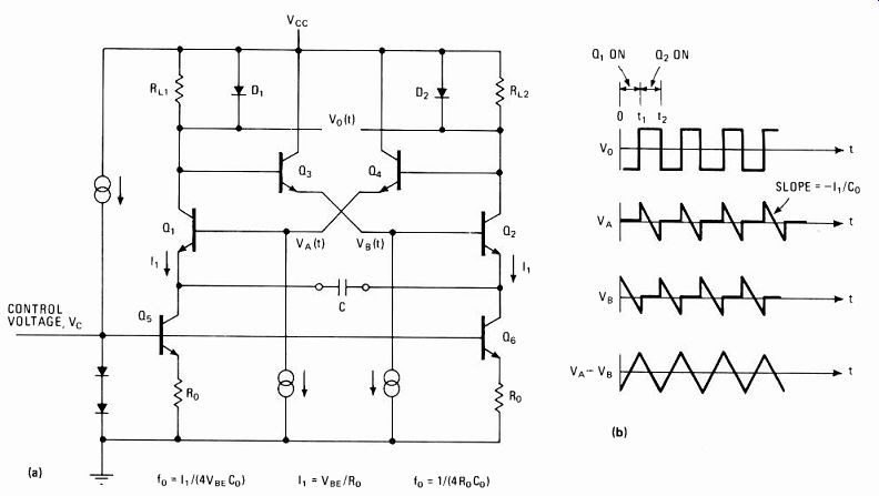
----------- 4. High frequency. An emitter-coupled multivibrator oscillator
(a) allows the generation of waveforms (b) of up to 20 megahertz.
Unfortunately, this type of circuit is difficult to compensate for changes in temperature, leading to poor stabilities at high frequencies.
The frequency can be controlled by varying II by means of a control voltage, Vc. The symmetry of the triangular and square-wave outputs can be offset by changing the ratio of emitter resistors of Q5 and Q6. This ratio effec tively changes the ratio of the current that charges capacitor C to the current that discharges it. In this manner, the triangular- and square-wave outputs can be converted to sawtooth or pulse waveforms.
The emitter-coupled multivibrator circuit shown is widely used for high-frequency applications. Oscillator types NE560 and NE562 from Signetics and others, as well as Exar phase-locked loops type XR-S200, XR-210 and XR-215, use it. The Exar XR-205 monolithic wave form generator also uses a similar emitter-coupled asta ble multivibrator design.
Strong temperature dependence
The frequency of this emitter-coupled multivibrator circuit is a function of VBE, which in turn is strongly dependent on temperature. To overcome this strong tem perature dependence, the timing current 11 is also made a function of VBE, such that It = VBE/Ro. Thus to a first-order degree, fo is temperature-compensated and is expressed as:
fo = (VBE/Ro)/(4VBEC) = 1/(4RoC)
This compensation is only effective at the center frequency. Since the control current that modulates the frequency is not compensated, even very small control current deviations degrade the temperature coefficient drastically (typically ± 300 ppm/C at ± 10% current deviation).
Despite center-frequency compensation, the emitter coupled multivibrator still exhibits a temperature coeffi cient of 200 to 300 ppm/°C. The culprits are the charging-current imbalance in Q1 and Q2 near the switching thresholds and the switching transients. The transients depend on circuit resistances, transistor transconduct ances, and input resistances, which all are temperature sensitive. Temperature drift of the circuit is inherent in its emitter-coupled multivibrators. There are othercom pensation techniques that can be used to make a high-stability (typically 50 ppm/°C or less) oscillator out of the circuit in Fig. 4a, but this is usually achieved at the expense of speed.
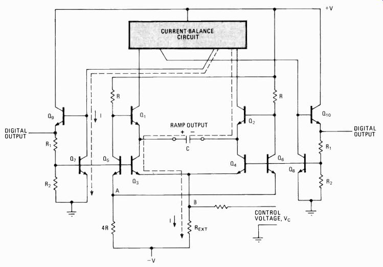
Improving temperature compensation Two very stable temperature-compensated oscillator configurations are used in Exar's XR-2206 and XR 2207 function-generator ICs as well as in the company's XR-2211 and XR-2212 phase-locked-loop ICs. They use a temperature-compensated emitter-coupled astable multivibrator circuit that has a typical temperature sta bility of 30 ppm/°C (Fig. 5).
Timing current, I, set up by Rem, flows in Q2, C, and Q3 when transistors Q5, Q7, and Q9 are on. The timing current is inverted by the current balance and establishes an identical emitter current density in Q. The voltage at the control input B is thus held at 0 over a wide range of timing currents. At an optimum current value, point A is also at 0 v, eliminating the temperature coefficient intro duced in this area. When the state changes, I flows in Q1, C, and Q4; all the compensation transistors on the right are turned on; and I is inverted by a current balance. As a result, I establishes an identical emitter current density in Q10.
------------ 5. Compensation. Emitter-coupled astable multivibrators
can be stabilized using this temperature-compensated circuit. Typical
temperature stabilities of 30 parts per million per *C are possible.
This circuit is used in Exar's XR2207 function-generator and XR2211 PLL
chips.
--------- 6. Clamped. The emitter-coupled multivibrator in Analog
Devices' AD537 voltage-to-frequency converter relies on another temperature-compensation
method. The collectors of Q1 and Q2 are clamped and a differential reference
voltage across them charges capacitor C.
The instability introduced by a shift in the regeneration point arising from dVBE/dT (where T is tempera ture) in Q1 and Q2 is minimized by the current balance, which forces the currents in these two transistors to be equal at the switching point.
The square-wave output is obtained differentially at the emitters of Q9 and Q10. A linear ramp is obtained across capacitor C. The frequency of operation is given by f = 1/(CRe,) and can be controlled by modulating the current, I, via the control voltage, Vc, applied to control node B.
Clamped collectors
Another temperature-compensated emitter-coupled multivibrator, used in Analog Devices' AD537 voltage-to-frequency converter chip, is shown in Fig. 6. In this precision collector-clamping scheme, a differential voltage, VR, generated by a bandgap reference circuit, appears across the collectors. VR is independent of the current, the temperature, the absolute value of VSE, and the supply voltage. This precise reference voltage is then transferred to the timing capacitor via two-stage emitter-followers A1 and A2 and transistors Q1 and Q2. Thus, the capacitor charges to 2VR twice each cycle, yielding a frequency expression of f = 1/(4CVR).
To compensate for the temperature drift mechanisms inherent in emitter-coupled multivibrators mentioned earlier, a small temperature coefficient in the opposite direction is deliberately added to the voltage reference VR. Using this technique, excellent stabilities of around 20 ppm/°C are possible.
After the generation of a basic waveform such as a triangular or square wave, the next step is to convert the waveform into a low-distortion sine wave. A triangular wave is usually preferred over a square wave, since the former's harmonic content is significantly lower. This initial harmonic content is further minimized by using a symmetrical triangular waveform that has negligible even-harmonic content. Such a waveform can be converted into a sine wave by rounding off its peaks. This is generally accomplished in one of two ways, each of which is suitable to monolithic integration.
Converting into a sine wave
One method involves a piece-wise linear approximation using breakpoints to round off the triangle wave.
This is usually done by diode-resistor or transistor resistor circuits. A disadvantage of these types of wave shaping circuit is that the input signal level, active device characteristics, and resistor ratios must be accurately controlled.
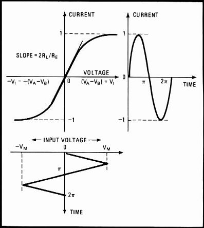
The other common method of converting a triangular wave into a sine wave is through the gradual cutoff of an overdriven differential transistor pair with an appropriate value of emitter resistance.
The differential gain state of the transistor pair used to generate the triangular wave can be adjusted to produce an overdrive condition by decreasing emitter resistance to a point where the input transistors are driven into cutoff. Figure 7 shows the voltage-current transfer characteristics of a such an overdriven circuit, with a triangular-wave input and a resulting sinusoidal output. The gradual transition between the active and the cutoff regions is logarithmic. Thus the triangular wave is amplified linearly near the center but logarithmically at the peaks. As a result, the sharp peaks of the input signal are rounded off and it is transformed into the desired sine wave.
The advantage of the second approach is circuit simplicity. However, it also requires a constant-amplitude input adjustment for low distortion at a given emitter resistance. Both methods can, with adjustment, provide total harmonic distortions of less than 0.5%.
The last building block of the typical waveform generator in Fig. 1 is the modulator section. For function generator applications, balanced modulators are preferred over conventional mixer types. Balanced modulators offer a high degree of carrier suppression and can be used for suppressed-carrier modulation, as well as for conventional double-sideband amplitude modulation. A simplified circuit diagram of a balanced modulator cir cut is shown in Fig. 8a. It is used almost exclusively by manufacturers of this type of IC because of its versatility and suitability for monolithic integration. In addition to performing amplitude modulation, this circuit also functions as a linear four-quadrant multiplier and phase detector. The balanced modulator's phase and amplitude transfer characteristics are shown in Fig. 8b.
------------ 7. Sins shaping. A common method of converting a triangular
wave (bottom left) into a low-distortion sine wave (right) is through
the gradual cutoff of an overdriven differential transistor pair, whose
transfer function is at top left, with an appropriate emitter resistance.
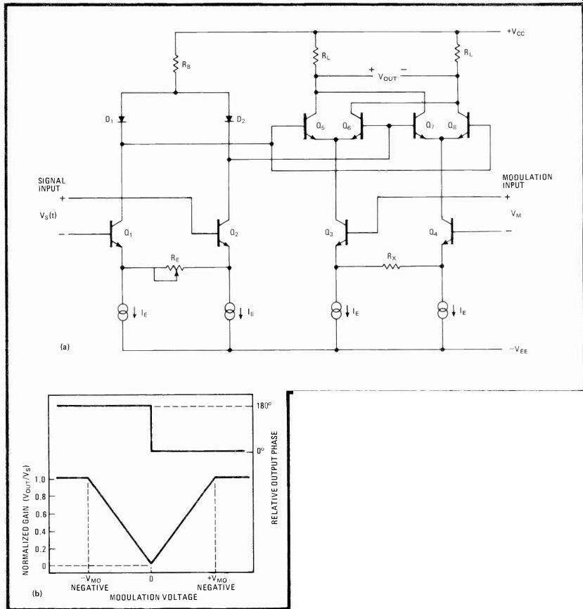
------------- 8. Modulation. For function generation, a balanced modulator
(a) is preferred for its higher carrier suppression and flexibility.
Used nearly exclusively by makers of IC function generators, this modulator
has the phase and amplitude transfer characteristics shown (b).
Timers also work like oscillators
The well-known 555 timer IC operates much like the RC multivibrator low-frequency oscillator circuit of Fig. 2a when in its astable mode. The only difference is that resistor R2 is in series with RI, in place of R1 alone.
Switch S1 is hooked up between ground and the connection between and R2. Again, operation is by the same charge-and-discharge cycle of capacitor Co, except that the charging voltage is passed through the series combi nation of R1 and R2, instead of R1 only. The output of the timer circuit is thus determined by the total resist ance of R1 and R2 divided by the capacitance of Co.
When the upper threshold of the timer circuit is reached, the circuit's output goes low and S1 is turned on, discharging Co to ground through R2. When the voltage reaches the lower threshold level, the threshold detector is triggered to begin a new cycle. During the discharge period, which is determined by R2CO3 the output stays low, allowing a digital output waveform to be generated. If R, is made very small in value compared with R2, the output becomes a square wave. As it is in the low-frequency oscillator circuit, the waveform across Co in a timer circuit is an exponential ramp.
When the circuit of Fig. 2a is combined with a one shot multivibrator circuit, a voltage-to-frequency con verter is the result. As shown in Fig. 9, the voltage comparator first compares the input voltage V, with VB.
When V1 is greater than VB, the comparator turns on the multivibrator, whose output will then go low for a timing period T, causing current source Io to turn on. At the end of the period, the multivibrator output goes high and Ic is turned off.
V-f converter cycling
As long as V8 is not greater than V1, the multivibrator keeps turning on and off for T-length durations until a sufficient charge (determined by the product of Io and T) is injected into the RB and CB network to cause VB to become higher than V1. When that happens, 10 stays off and VB decays until it equals V1. This completes one cycle, and the V-f converter runs in a steady-state mode.
In the steady-state mode, Io charges CB fast enough to keep VB equal to or greater than V1. Since the discharge rate of CB is proportional to VB/RB, the frequency at which the circuit runs is proportional to the input voltage. The circuit's output is a series of pulses, with the length of durations, T, determined by the external RC components of the multivibrator.
Isolator stretches the bandwidth of two-transformer designs
Stable and linear isolation-amplifier approach now suits many applications in which analog signals up to 15 kHz must be handled, such as motor control
by Bill Morong, Analog Devices Inc., Norwood, Mass.
The list of applications requiring the isolation of analog signal sources from data-processing circuitry is a long one and growing. These diverse applications place widely varying demands on the isolation scheme used, so it is not surprising that many different isolation techniques have been developed to meet those demands.
Transformer and optical isolation methods are two of the most common routes taken. Two-transformer isolators, though outstanding in terms of linearity and stability of gain and offset, are generally shorter on bandwidth than single-transformer or optical isolator designs. The arrival of a wideband two-transformer amplitude-modulated isolation amplifier, the model 289, opens up a number of formerly impractical applications to the two-transformer technique.
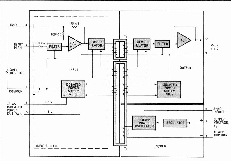
----------- 1. Isolated. A favorable cost-performance compromise between
optically coupled and single-transformer isolation amplifiers is achieved
by the wideband two-transformer model 289 isolation amplifier. It owes
much of its high performance to its input and power isolation schemes.
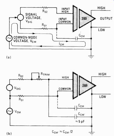
---------- 2. Common-mode. Finite capacitance across an isolation
amplifier's isolation barrier limits common-mode rejection (a). Adding
capacitor CCM' and resistor RTRihi as in (b) causes the common-mode voltage
across Rs2 to cancel the common-mode voltage across Rs..
---------- 3. Process control. A two-transformer isolation amplifier
is sufficiently linear to isolate floating transducers from computerized
process-
control equipment. The analog-to-digital converter used must be monotonic to guard against instability in closed-loop systems.
Any application in which low-level analog signals must be detected in the presence of high common-mode voltages requires isolation; circuits in which ground-loop currents can introduce large errors in the signal being measured are also candidates. Proper isolation allows the transmission of a signal across a nonconducting barrier without a galvanic or electrical connection.
Of the wide variety of isolation techniques now in use, optical and magnetic isolation schemes are by far the most common in all but highly specialized applications.
A knowledge of their strengths and weaknesses is important for a designer faced with isolation problems.
A typical transformer-coupled isolation amplifier incorporates an oscillator to generate the carrier signal.
The isolation amplifier's input modulates this carrier.
The input signal can be any frequency within the pass-band of the isolation amplifier-including dc. The modulated carrier is passed through a signal transformer and demodulated, where a replica of the input signal is reconstructed at the isolation amplifier's output port.
The second transformer
Transformer-coupled isolation amplifiers often contain a second transformer that makes the unmodulated carrier signal available on both sides of the isolation barrier. This unmodulated carrier signal is used to facilitate modulation and demodulation and to generate dc power to energize the isolation amplifier's input or output circuitry. It can sometimes be used for powering external circuits.
Two-transformer isolation amplifiers have been avail able for a long time and are convenient to use. They feature input-offset drifts of a few microvolts per °C, gain-temperature coefficients under 50 parts per million per °C, and gain nonlinearities of less than 0.01%. Long- term stability of these parameters is also excellent. But they have had one major limitation: bandwidths of not much more than 3 or 4 kilohertz.
For higher bandwidths, optically coupled isolation amplifiers were developed that have bandwidths up to 15 kHz. In such isolation amplifiers, the input signal modulates the intensity of beams of light generated by light-emitting diodes. The modulated light beams impinge upon light-sensitive diodes that generate output currents roughly proportional to the intensity of the impinging light. In optically coupled isolation amplifiers, the current from the light-sensitive diodes is fed to circuitry that converts it into an isolation-amplifier output voltage.
Other light-sensitive diode currents are fed back to the isolation amplifier's input circuit to help remove gain nonlinearity and instability normally introduced by the variations in the transfer efficiency of the LEDs, the optical path, and the light-sensitive diodes.
Besides extending bandwidths, optical isolation amplifiers also have input offset drifts and gain temperature coefficients similar to those of transformer-coupled units. One drawback, however, is a long-term gain shift that is typically an order of magnitude greater than that of transformer-coupled isolators. That shift is caused by aging of the optical components.
Another drawback is that although optical isolators require no carrier signal, a separate dc-dc converter is needed to power the amplifier's input and output circuits. This hurts the cost advantage of an optically coupled isolator over a transformer-coupled one.
Wideband transformer-coupled isolation amplifiers have been introduced in which the functions of separate signal and power transformers are combined into a single transformer. Such isolation amplifiers feature about twice the bandwidth of optically coupled units andcom parable nonlinearities. They are also less expensive. But they suffer from increased offset drift and the generation of excessive noise in the modulation-demodulation pro cess. And they are also susceptible to semi-permanent shifts of electrical characteristics when subjected to strong magnetic fields that are later removed.
Improvements in the design and construction of trans formers allow the model 289 two-transformer isolation-amplifier module to offer 15-kHz bandwidth and retain the approach's traditional strengths-excellent isolation and good dc characteristics. Packaged in a 2.25-cubic-inch plastic case, this three-port isolator (Fig. 1) contains a dc-dc converter for isolated ± 15-volt power-supply lines, an output-port buffer, and a current-limiting regulator that allows operation over a wide range of supply voltages without any degradation in performance.
--------- 4. Data acquisition. Where many transducers are powered
by a single low-voltage supply, a multiplexer can be used to feed into
a single isolation amplifier. This circuit is only useful for cases in
which the potential between transducers does not exceed 30 volts.
----------- 5. Patient isolation. Although many isolation amplifiers
are used in electrocardiograph patient-lead isolation, few have the bandwidth
for applications like electromyography and pacemaker-pulse analysis--but
the 289 is wideband enough for these medical uses.
The 289 represents a favorable cost-performancecom promise between optically coupled and single-transform er isolation designs. An error budget has been calculated for all three approaches (see "A comparison of error budgets," p. 156). Although the small-signal bandwidth of the dual-transformer method employed in the model 289 is less than that of the single-transformer design, gain nonlinearity and gain change with temperature of the former method are as good, if not better. Moreover, offset-voltage changes with temperature are by far the lowest with the two-transformer design.
The presence of a carrier signal in a transformer coupled isolation amplifier inevitably leads to a carrier ripple component in the isolation-amplifier's output. As the bandwidth of an isolation amplifier becomes a larger fraction of its carrier frequency, ripple becomes more difficult to control. Despite this fact, the 289 isolation amplifier produces less ripple than many other trans former-coupled isolation amplifiers having much less bandwidth. This low ripple level means less need for output filtering.
Holding down ripple
To keep power-supply ripple from modulating the isolation-amplifier's carrier signal, voltage regulators should be used. Some isolation amplifiers have built-in regulators, not only to eliminate power-supply ripple effects, but also prevent carrier-frequency spikes from being broadcast to the rest of the system via the isolation amplifier's power terminal.
Another potential problem is that of output loading.
For many isolation amplifiers with unbuffered output impedances of 1,000 ohms or more, the use of low impedance loads can lead to large gain errors. The use of external output buffering is recommended in such cases.
Of course, those isolation amplifiers with internal output buffering eliminate the need to do so.
Three-port isolation amplifiers are easier to apply than two-port ones, since the latter have their power-supply and output-port returns through a common terminal.
But even three-port ones are not all of the same construction and thus offer differing degrees of isolation between output and power ports. For example, some three-port isolation amplifiers have their power-supply and output ports connected by a capacitor. The capacitor permits carrier current to pass but blocks dc, allowing moderate levels of output common-mode voltages. however, the carrier signal's return through external circuits can introduce ripple currents into those external circuits.
True three-port isolation amplifiers like the model 289 have galvanically isolated ports between which neither ac nor dc can flow. Their outputs can be connected to common-mode voltages of either polarity, within the output common-mode voltage range of the isolator.
Certain precautions must be observed when applying isolation amplifiers. The most obvious is that the circuit in which the isolation amplifier is used must be wired in such a manner that the amplifier's isolation properties are not lost. This means that adequate spacing must be provided between input and output circuits.
Maximizing common-mode rejection The conversion of common-mode signals into normal-mode ones at the input to an isolation amplifier limits the common-mode rejection of the amplifier to some finite value. A certain amount of capacitance exists between circuitry on either side of the isolation barrier, and it causes a common-mode current to flow when a common-mode voltage is applied across the barrier (Fig. 2a). This common-mode current is proportional to the applied voltage of the common-mode signal, its frequency, and the barrier capacitance.
--------- 13. Motor control. The 289 isolation amplifier has sufficient
bandwidth and low enough phase shift to be used in motor and ac load-control
applications. Two isolators are used, one to sense motor current and
another to feed armature-voltage information to the controller.
For most isolation amplifiers, the common input terminal forms a more direct path for the common-mode current caused by the barrier capacitance than the high input terminal, so most of the common-mode current flows through the common input terminal. If a normal-mode signal source with two equal output resistors is connected to an isolation amplifier as shown in Fig. 2a, a common-mode-induced normal-mode signal appears in series with the signal source and is treated by the system as a normal-mode signal.
One way to minimize the effects of common-mode currents is to interpose a shield in the isolation barrier to intercept common-mode currents and divert them around the input-source resistance. Another method is to employ a differential input stage ahead of the isolation amplifier. These techniques, however, may be limited for those cases where physical space is at a premium and little room is available for shields or additional input stages. In such cases, common-mode rejection can be maximized by minimizing the capacitance value across the isolation barrier.
For applications in which the source resistance is known and is relatively constant, large common-mode-rejection improvements can be obtained at little extra cost using the circuit of Fig. 2b. Adding capacitor Ccw causes more common-mode current to flow in RS2 and RTRIM. The proper adjustment of RTRIM can develop a voltage in series with the high input terminal that can cancel the common-mode-induced voltage across RS1.
The penalty for this approach is a small increase in common-mode current (about 0.25 microampere at 117 volts, 60 hertz). Ccw must be capable of withstanding the full common-mode voltage across the isolation amplifier.
Using a lengthy cable to connect a high-impedance device to the input of an isolator exacerbates the problem of converting common-mode signals into normal-mode ones and opposes the cancellation obtained in Fig. 2b. The use of a long cable between signal source and isolation amplifier should therefore be avoided.
When data must be acquired from floating transducers for computerized process-control systems, a two-transformer isolation amplifier like the model 289 may be used for potential differences or to interrupt ground loops among transducers or between transducers and local ground levels (Fig. 3).
In process control Since the isolation amplifier and the analog-to-digital converter are likely to be included in a large feedback loop, the converter must be monotonic and isolation must be sufficiently linear not to induce non-monotonic behavior. Lack of monotonicity can cause instability in the feedback loop.
----------- A comparison of error budgets A comparison of error budgets for the three most common analog isolation schemes-two-transformer designs such as the model 289, optically coupled hybrid amplifiers, and single-transformer amplifiers-shows clearly the first technique's advantages over the other two. The following calculations are based on the summary of major specifications listed in the table. For the sake of brevity, only major error sources are treated. Calculations are for a circuit with unity gain, with an output of 10 volts full scale ( ± 5 V).
Operation is at 25°C ± 25°C, and it is assumed that initial gain and offset errors are trimmed out.
A gain temperature coefficient of 0.005%/°C multiplied by a 25°C span yields 0.125% of full scale for the dual-transformer scheme (listed first in the table). Next, input and output offset voltages as a function of temperature, ± 10 and +50 microvolts/°C yield 1,500 AV, which is 0.015% of the 10-V full-scale output. The new error sum is now 0.125% (gain temperature coefficient) plus 0.015% (offset voltage), which equals 0.14%. Add to this gain nonlinearity of 0.01%, and the total error becomes 0.15% of full scale.
The gain temperature coefficient of the second design, with optical coupling, is the same as that of the dual-transformer scheme-0.125% for a 25°C span. The 455 AV/°C offset voltage multiplied by 25°C yields 11,375 AV, which is 0.114% of 10 V. When the linearity error of 0.05% of full scale is added, the total (0.125% + 0.114% + 0.05%) is 0.289%.
For the third, single-transformer design, the gain temperature coefficient of 0.006%/°C multiplied by a 25°C span yields 0.15% of full scale. The 525-AV/°C offset voltage multiplied by 25°C yields 13,125 /Ai, which is 0.13% of 10 V. When the linearity error of 0.05% of full scale is added, the total (0.15% + 0.13% + 0.05%) comes to 0.33%.
For gains other than unity, the calculations become more complicated. The stability of user-supplied gain resistors can affect the amplifier's gain stability, so the effects of these must be included. (This is also true at unity gain for isolation amplifiers in which gain is set to unity by user-supplied resistors.) At different levels of isolation-
amplifier gain, offset drift varies, further complicating error-budget calculations. For example, the first isolation scheme has less total offset drift below a gain of 80 than the second. Above a gain of 80, the second scheme has less total offset drift than the first. And the third, the single-transformer design, has more offset drift at all levels of gain than the other two.
Other complicating factors include errors caused by input-difference current and by noise. For applications involving low source resistance, these errors are small enough to be negligible. If, however, it becomes necessary to add resistors in series with the input of an isolation amplifier for differential-overload protection, these errors may become large enough to merit consideration.
Because the input structures of different isolation amplifiers vary greatly, including these errors in the above calculations is very difficult if not impossible.
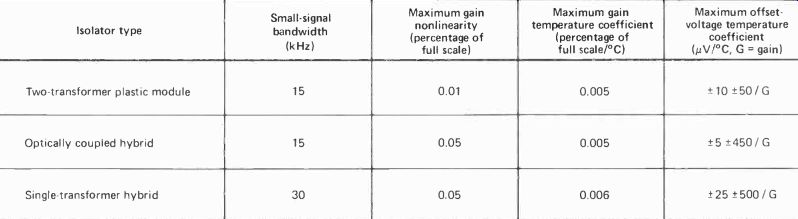
----- PERFORMANCE COMPARISON OF THREE ISOLATION AMPLIFIER TYPES
--------- In using the circuit of Fig. 3, it is desirable that the isolation amplifiers be protected against differential input overloads. Otherwise, mis-wiring the amplifiers to the ac power line can cause them to fail. Furthermore, the isolation amplifiers should be synchronized to avoid errors caused by beat-frequency signals generated by the mixing of the amplifiers' individual carrier frequencies.
The connection of the synchronization terminals in Fig. 3 achieves this purpose. This circuit suffices for common-mode voltages up to 2,500 v peak, ac or dc.
In a data-acquisition system in which multiple transducers are powered by a single supply and the voltage level of that supply is sufficiently low that a multiplexer can handle all of the transducers' voltages, a lone isolation amplifier and a multiplexer can be used (Fig. 4).
In the past, such a configuration has not been generally possible because of the speed limitations of the isolation amplifiers available. The model 289 isolation amplifier, however, has a sufficiently short settling time to make its use practical in this circuit.
The approach shown in Fig. 4 is useful when the voltage difference between any two terminals of the transducers does not exceed 30 v. A limitation of this circuit is that, though the input of the isolation amplifier is protected against ac power-line voltages, the amplifier's power terminals as well as the multiplexer are not.
Addressing of the multiplexer in Fig. 4 is binary, with an enable signal being provided for the selection of the signal-source circuit. Digital signals are optically isolated. For several groups of transducers, several circuits may be used as in Fig. 4, in which case the isolation amplifiers are synchronized for operation. And if several transducers share the same common terminal, that terminal can be attached to the input common of the isolator, halving the number of switching elements.
In wideband vibration analysis, a strain gage may be bonded to a mechanical member that is subject to stress.
Strain produced in the mechanical member is transmitted to the strain gage. Since the gage must be intimately connected to the mechanical member, it may be desirable to isolate its output. For cases in which the frequencies of interest extend much beyond a few hundred hertz, a wideband isolation amplifier like the model 289 can be used. The use of variable filters at the isolation amplifier's output stage makes it possible to view on an oscilloscope particular frequency spectra.
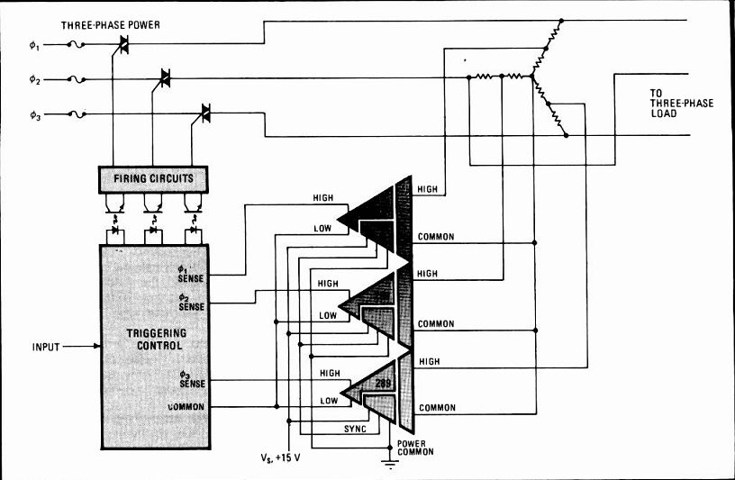
--------------7. Three-phase. Three dual-transformer isolation amplifiers
can be used in a control circuit for a three-phase ac load. Each amplifier
senses a line's voltage, produces a replica of the waveform sensed, and
provides this replica waveform to the trigger-control circuit.
Medical applications
The 289 is useful in medical applications such as patient isolation. Although many isolation amplifiers are used in electrocardiograph patient-lead isolation, few have the bandwidth necessary for use in electro-myography or for the analysis of pacemaker pulses.
The circuit of Fig. 5 is useful for such applications. A differential amplifier is connected to the isolation amplifier's input. This allows the 289's common input to be connected to the patient so that the patient's common-mode voltage drives the amplifier. A balanced input structure reduces the normal-mode noise that is converted from common-mode noise.
The circuit's FET inputs allow the use of large-value input-protection resistors without affecting noise performance. These input resistors, along with the clamping diodes, protect the isolation amplifier's input structure from defibrillator pulses and protect the patient from fault currents that can develop in the event of the failure of a preamplifier component.
The differential input of Fig. 5 is converted into a single-ended input suitable for use by the isolation amplifier. The gain stage used for this conversion does not make use of unduly high impedance values, thus minimizing noise generation. The input diode should be of a low-leakage type and must not be light-sensitive lest photocurrents be generated in the input structure.
In any patient-lead isolation application, wiring on the patient's side of the isolation amplifier is as critical as the isolation properties of the amplifier itself. Since this wiring is an extension of the patient's vulnerable area, its proper selection is critical. For example, some cables produce copious noise when flexed, thus ruining the otherwise noise-free performance of an isolation system.
Cable length can also be a problem. A few tens of feet of patient cable along a concrete floor can entirely bypass the capacitive isolation of the amplifier.
For motor and ac load control, the use of two-transformer-coupled isolation amplifiers has not usually been possible because of such amplifiers' bandwidth limitations. Thus optically coupled isolation amplifiers equipped with floating power sources to energize their input amplifiers have been used. The two-transformer design used in the model 289 makes it possible to use transformer-coupled isolation amplifiers for motor and ac load-control applications. This amplifier possesses sufficient bandwidth and low enough phase shift to make its use practical in such applications.
Faithful replication
Figure 6 shows two dual-transformer isolation amplifiers sensing the armature voltage and current of a motor. Faithful replicas of the waveforms of these variables are delivered to the motor control. Isolation amplifier A1 operates at unity gain from divider RI-R3 to deliver an output that is 1/100 of the armature voltage.
Isolation amplifier A2 operates at a gain of 100 to deliver a voltage that is 100 times that developed across the current-sensing resistor.
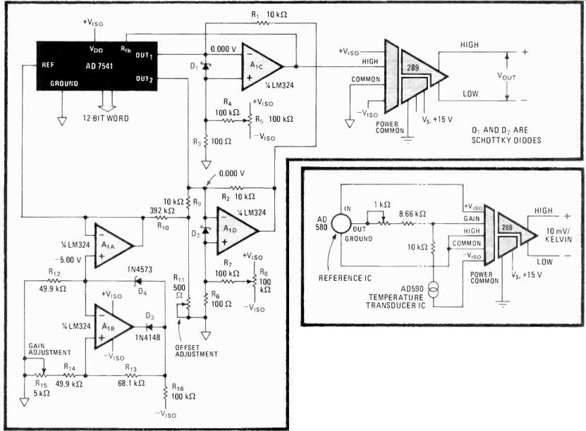
------------ 8. Converter. The 289 two-transformer isolation amplifier
can be used to isolate the output of a 12-bit digital-to-analog converter.
Resistors R5 and R8 should be adjusted to produce less than 0.5 millivolt
at both d-a converter outputs for this circuit to work properly.
------------9. Temperature. To measure the temperature of an object that may float at a high common-mode voltage, a dual-transformer isolation amplifier can be used. All connections to the isolation amplifier's gain terminals should be kept as short as possible to minimize errors.
Figure 7 shows three dual-transformer isolation amplifiers sensing the voltages on the three lines of a three-phase ac load. The Y network divides the voltages of the three phases and creates a neutral for the input commons of the isolation amplifiers. The output of each isolation amplifier is a faithful replica of the waveform of the phase that it senses. The isolation-amplifier outputs provide the feedback necessary for the trigger control to correctly fire the triacs. These same outputs could also be fed to root-mean-square-to-dc converters in similar ac load-control applications.
A note of caution on the use of the circuit of Fig. 7:
since transformer-coupled isolation amplifiers are susceptible to applied magnetic fields, it is best to place them outside the leakage fields of motors, transformers and other sources of magnetic interference. If this is not done, these magnetic fields can modulate the signals passing through the isolation amplifiers.
Figure 8 shows a dual-transformer isolation amplifier providing a 12-bit d-a converter with isolated output-
voltage capability. A buffered- 5-v reference voltage is provided to the converter by amplifiers Ala and Alb and their associated circuitry. The fractional value of a digital-word input to the converter causes a proportional fraction of the d-a converter current to flow in the converter's OUT1 output terminal. The remaining converter current flows into the converter's our2 terminal.
Current flowing into OUT, causes a positive voltage at the output of amplifier A1.. Current flowing into OUT2 of the converter causes a positive voltage at the output of Aid, in turn causing a negative voltage at the output of A ic. The output of A1, is reproduced at the output of the isolation amplifier.
For the circuit of Fig. 8 to work properly, resistors Rs and R8 must be adjusted to produce less than 0.5 millivolt at both d-a converter outputs. Resistor R15 can be used for gain adjustment, while resistor R11 can be used to adjust the output offset between an input binary code of 100000000000 and one of 0. Circuit operation is bipolar with a ± 5-v swing.
Measuring floating temperatures
A dual-transformer isolation amplifier like the 289 may be used in applications where it is necessary to measure the temperature of an object that may float at a high common-mode voltage, as shown in Fig. 9. The isolation amplifier provides a ground-referenced output.
In the circuit of Fig. 9, the temperature sensor sinks a current of-1 microampere per kelvin. This current flows from the gain terminal of the isolation amplifier, developing across the amplifier's internal feedback resistor a voltage of + 10 millivolts/K. This voltage appears at the isolation amplifier's output.
For an output of 10 my/°C, the circuitry shown with a dotted connection can be used. A current of + 273 MA is sourced through the 8.66-kilohm resistor and the 1-kS/ potentiometer, canceling the temperature-sensor current at 0°C (273 K). This results in 0 my at the amplifier output at 0°C.
For proper operation of the circuit in Fig. 9, all connections to the isolation amplifier's gain terminals should be kept as short as possible.
[source: ISBN 0-07-606808-0 Copyright© 1982 by McGraw-Hill, Inc. ]