How Floppy Disk Systems Work
Sooner or later just about every serious computer hobbyist reaches their computer's memory limit. There are some applications that require too much I/O action to be practical with a cassette based system or require too much memory space to fit in a RAM. It's this need for high-volume storage and rapid access time that makes a hobbyist disk system desirable. These systems don't come close to commercial hard disk systems in terms of performance but they can easily fill the computer hobbyist's memory bill.
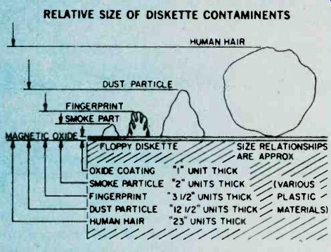
----------- RELATIVE SIZE OF DISKETTE CONTAMINENTS---The metal oxide surface of a floppy disk is very sensitive to contamination. Each one of these contaminants (right) could cause a dropped bit. Since the disk is always kept in it's protective envelope, this is usually not too much of a problem in daily usage.
Floppies have become the missing link to a midrange of random access memory systems. The floppy offers higher performance at lower cost than cassette and similar types of Input/Output (I/O) devices.
Well Packaged. The present standard floppy is an 8-inch flexible disk of a plastic material coated with a magnetic oxide. Looking a little like a popular 45 RPM record, it is sealed inside a jacket and there are no grooves on the surface.
The disk cannot be removed from the jacket which is designed to protect the recording surface. The disk is visible at a slot, a spot, and a hole in the center of the jacket. Users are told by the instructions that we must not touch exposed areas of the disk or write on it with anything firmer than a Q tip. Finally the user is admonished to return the jacketed disk to its outer envelope after they have finished using it.
The natural skin oil of fingerprints can damage the quality of music in needle and groove recordings, and in the super-miniature world of floppies, a fingerprint can destroy an entire segment of data. A dust particle can waste a dozen sectors and a human hair can reduce the effectiveness of the Read/Write/Erase (R/W/E) heads.
It is understandable why the media, as the flexible disk is sometimes called, is permanently sealed with all of those implicit instructions. There is, however, an internal jacket wiper that continually cleans the rotating disk and removes contaminants, and floppies are reasonably rugged.
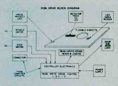
Hardware. The disk-drive hardware is add-on equipment to the main frame of the computer. Inside the drive are motors, driving mechanisms, and interfacing electronics that enable the drive unit to "talk" with the controller.
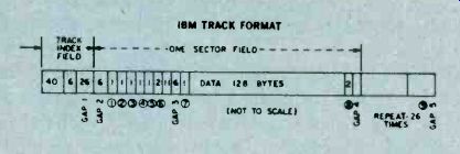
The diskette is inserted into the drive unit through a small door in the front. Once the door is shut, it is locked by the drive unit logic until the door release button is pushed to disable the drive assembly. The drive spindle centers and grasps the center of the diskette firmly as the motor comes up to speed. During power-up the diskette reaches a speed of 360 RPM, and R/W/E heads are stepped out to track 00 and a mechanical index hole provides the first location pulse for disk timing. In the IBM format this is the only reference to a physical location on the disk.
The floppy is firmly held against the recording surface, and the heads are positioned by a precise stepping motor. While the heads are positioned over the desired track, they ride above the spinning diskette. Once the correct track is located, in what is called a "seek operation," a head loading coil pulls the heads down onto the magnetic surface. This operation is called loading the heads and it is controlled by a computer program.
When the heads are to be moved again, in another seek operation, to a new track, they are first unloaded, stepped to a new track, and then reloaded to a new track.
This requires about three milliseconds per track of movement. It will further require about 50 milliseconds, per track, to move the heads and about 15 milliseconds of settling time.
Part of System. Floppies should always be thought of as a part of a sophisticated cluster of mechanical drivers, computer electronics, and software called a computer.
Fundamentally this computer consists of a central processor unit (CPU), some memory, some interfacing devices, called controllers here, and an entry device such as a keyboard CRT, and some software.
Computer operation is made possible by a written program entered into the computer's memory and operated on by the internal microprocessor. The programs are fed by any one of a number of techniques: a paper tape punch, keyboard, cassette tape, or teletype.
All of these are slow and time consuming. New ways are continually being introduced to feed the voracious appetite of computer memories. Floppies are the most versatile of the program instruction loading techniques In a computer's time frame things go on a million times faster than in our brain's time frame. In such a whirlwind existence, telling computers what to do was a difficult problem. The answer was in the development of software which the computer could store in memory for reference each time it needed a new program instruction.
--------- READ/WRITE/ERASE OPERATION--There is no physical track on the disk as with an LP record. The tracks are formed by the passage of the record (write) head over the surface of the disk. The disk itself appears to be a solid sheet of recording tape material.
Software. The computer-the IC's, printed circuit boards, filter capacitors, chassis, and power supply-are all part of the hardware. All of this state-of-the-art electronics is just so much junk without a program, a way to make the computer compute. The instructions, written in computer languages, are called software.
We talk with the floppy (human to floppy) through a series of interpreters comprised of software and hardware. First we place our instructions, using perhaps, Fortran in a machine assembly language. Located within this language and acting as a general interpreter, is a section of software called a file manager. Its job is to take general instructions, count words to be put on the floppy, calculate the number of sectors, tracks and floppies that will be needed to store your file. All we do is to tell the file manager how much and where; it will do the rest. It will even put the data on the floppy then check to see if it got there, and if not correct its own errors. The special language of the computer is based on the numbers zero and one.
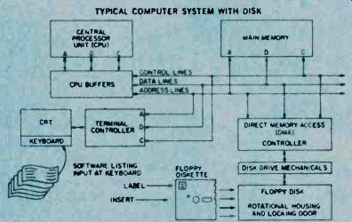
----- This block diagram of a typical computer system utilizing CRT readout and disk drive shows the parallel connections of the memory, drive controller and terminal controller.
YOU can easily see from this diagram how the physical configuration of the disk is related to the various electronic systems needed to control information storage and retrieval.
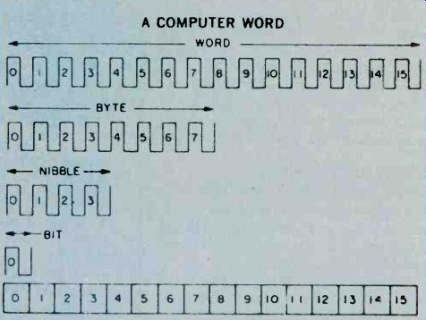
A COMPUTER WORD
Software is the artful manipulation of the WORDS, bytes, nibbles, and bits utilized in transferring something meaningful between humans and machines without resulting in the total disorientation of the two parties involved.
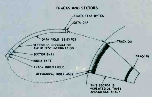
This diagram shows the relationship between track information and sector information as they are physically located upon the disk when utilizing the IBM-type disk formatting.
-------
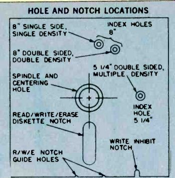
The disk's guide holes serve the same purpose as the arm on a record changer which positions the tonearm according to LP size.
======
These two values comprise one "bit" of information.
At this level there are no grey areas, no informational maybes. Facts are either a zero or they are a one. In this language a word has only one length of the microcomputer. It is 16-bits long. That is 16-bits having two states or thirty two pieces of information. However most peripheral devices, such as the floppy controller, that hunk of electronics that interfaces (talks) between the floppy and the CPU, is designed to speak in half words. This half word is called Byte, pronounced "bite." A byte has 8-bits so there are two bytes to a full 16-bit word computer.
The story doesn't stop here. A new term is emerging in the industry as they learn to manipulate the byte. It is the half byte and is called a nibble.
Disk Mechanics. The RAVIE slot in the floppy jacket is two inches long by ',-inch wide. That little hole on the opposite side (8 inch diskette) is the mechanical index hole, which is a physical starting place (read by a LED sensor) for recording information on the oxide surface.
On a tape cassette you can break off a plastic tab thereby preventing further over recording on that cassette. An industry term for this is `record protect.' Floppy disk jackets have this same feature, in a slightly different form. On some jackets there is a write protect slot cut in the paper of the jacket. When not needed the slot is covered over. This slot permits a photo-optical system to shut off the write electronics when the system detects a slot. In this way valuable programs already recorded are not destroyed by writing over the program.
With some drive units there is a switch to override this system, with other drives we must tape over the write protect slot.
The erase head most widely used may be either a tunnel-erase or a stradle-erase head. The tunnel-erase head design minimizes the influence of noise from data in adjacent tracks. This more clearly defines' the erase band and improves the signal to noise ratio. Present usage seems to favor the tunnel-erase head design.
To place information on the diskette (to write) and to retrieve information (to read) a software plan called a format is employed to pre-organize diskette data fields.
Where only a single reference is made to the mechanical index the resulting formatting is called soft sectoring.
Most of the information presented here 'is for a single density, soft-sectored, IBM formatted diskette. After receiving the pulse that represents the index hole, the rest of the floppy is formatted from the software, or computer program.
IBM Format. The IBM 3470 formatted diskette, one of the more popular industry standards, has 77 tracks, with 26 sectors, (data spaces) formatted per track. There are 128 bytes per sector, 256 nibbles, or 1024 bits. The total numbers of sectors per single density diskette is 2002. Of the tracks, 74 are for data storage, two are set aside as alternate "bad tracks reserves," and another track is reserved for maintenance purposed. A typical data transfer rate from floppy to controller is 250 kilobytes per second.
The tracks are numbered from the outside in with number 00 on the rim. Number 76 is the last track and is nearest the hub. Remember that there are no real tracks that you can see. They are the products of a software format, in this case IBM format 3470. These single sided, FM coded (more about that in a moment) disks can have a recording density of 3408 bits per inch.
A second type of sectoring is called hard-sectoring.
Thirty two holes are cut in the diskette. These become the index marks for each sectored area. There is a 23% increase in data packing in hard-sectoring but the industry seems to prefer the soft-sectored format.
The sectors each contain a data field, with data gaps Co guard this information, sector and track identification, again with gaps to protect this information, and guard bytes to further isolate sectors of information. All activity is in byte-length half-word groups.
Frequency Mod. The technique used to place data on the diskette is called Frequency Modulation (FM). Clock Pulses, 4 micro-seconds apart, from a 250-KHz clock generator, are placed on the floppy sectors forming data cells. This is the time from one clock pulse to the next: A magnetic transition within a data cell is read from the data stream as a one; no transition as a zero. The data bit will fall into the center of a 4 microsecond data cell.
When the controller performs a read operation, the data stream going back to the drive electronics and on to the controller where the data is separated from the clock pulses, a known frequency, and also the index mark, sector data, and addressing information is removed before sending the date on to the Central processing unit.
As you might imagine there are sometimes errors in either a read or a write operation. A software test program is designed to search out these errors. They will be classed as either hard or soft errors. That is an error traceable to a piece of hardware such as a faulty motor is a hard error. An error traceable to a poorly formatted sector will be a soft error. One possible soft error would be a bad sector such that data could not be written into the sector. The controller would store the address of that sector in a Bad-Sector file in memory and search out another sector. Later if the computer addressed that bad-sector, the file manager would discover that it was bad and immediately go to the address of the new sector used in place of the damaged one. At some future date the user.
might want to replace the floppy if there are too many bad sectors.
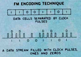
--------- FM ENCODING TECHNIQUE---The binary data pulse stream (lower line) is translated into and stored in the data cells (top line). 1's and 0's are shown.
------ IBM definitions: byte 1-address mark; 2-track #; 3-side #; 4-sector #; 5-sector size; 6-ID test bytes; 7-data mark; 8data test bytes; 9-trailing gap.
As the industry gets better at the techniques to pack and crunch data onto a small recording surface, floppy usage will increase. Shugart and Perteck, among others, are offering the double density floppy employing a recording code permitting double data packing using the MFM or Modified Frequency Modulation code. Two other codes now in use are the Modified MFM or the Group Code Recording (GCR) technique. Double sided recording heads have also been introduced allowing recording on both sides of the floppy with transfer rates of 500 Kilobytes per second and 256 bytes per disk sector.
Mini-Floppy. Hardly had this double density, double sided floppy been introduced when the mini-floppy popped on the stage. Only 5á inches in diameter, it uses a coding scheme called the Modified MFM, with the index hole shifted 90 degrees to the right. The Radio Shack add-on TRS Mini-Disk System, uses a mini floppy. Cost is about $500 for the "first Disk-Drive." As with all disk systems, a certain number of sectors are devotes to housekeeping, sometimes called labeling. Those sectors usually consists of a directory, test programs, and other sector and track information so that it will talk smoothly with its computer system.
The flexible diskette is a very useful peripheral device used with a 1/0 controller and can be used to store special diagnostics (hardware test programs) and debugging routines.
=====
=====
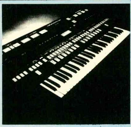
Synthesizer Science
There is no doubt that electronic synthesizers have made a major impact on the world of music, and are here to stay. No longer are they limited to experimental avant-garde works. There are dozens of albums of traditional music (both classical and popular) played on synthesizers, and they are widely used in radio and television commercials, and popular music of all kinds; rock, jazz, and even western.
A good synthesizer can take the place of literally dozens of other instruments, and can easily produce sounds that would be difficult, it not impossible, to duplicate on acoustic instruments. Synthesizers are fascinating to experiment and practice with.
Many people, however, are reluctant to try them, fearing they are too complex for the beginner.
Actually, synthesizers can be quite easy to understand, if you just take them one step at a time.
Synthesizers are really nothing more than packages of modules, that can be connected in various ways to produce different sounds. Once you understand the basics it's not hard to design an experimental synthesizer of your own.
Basically, there are four types of modules in synthesizers; oscillators, which produce the basic signal; filters, which modify the harmonic content, or tone of the signal; amplifiers, which modify the dynamics or volume of the signal; and, finally, some method of controlling all the modules.
You could use potentiometers to control all these devices manually (in fact, that is what the early electronic music composers did). That method is very awkward and tedious. Most modern synthesizers use some form of voltage control in their electronic circuit.
The voltage to a voltage-controlled oscillator (VCO) would control the frequency of the signal, or the pitch.
The voltage to a voltage-controlled filter (VCF) will determine how much of the original signal will be attenuated. The voltage to a voltage-controlled amplifier (VCA) determines the strength, or level of the signal.
Keyboards. There are a number of voltage sources that are used in synthesizers. The most common is the keyboard, which is similar to those found on pianos and organs. Figure 2 shows a simplified voltage control keyboard. Each switch is a key. If Si is closed, none of the resistors are in the circuit, so the full five, volts is available at the output. If S2 is closed, R1 is brought into the circuit, so the output voltage is dropped to a lower value For this example, let's assume all four resistors are rual, and each has a one volt drop across it. This means that closing S2 produces a four volt output. S3 would bring both R1 and R2 into the circuit (in series, so their values add), so the output would now be three volts. S4 would bring 3 resistors into the circuit, giving a two volt output, and S5 is connected to all four resistors, giving an output of only one volt.
One important thing to notice with this kind of arrangement, is that only one voltage can be produced at one time. That is, the keyboard is monophonic.
Polyphonic (multiple note) keyboards are used in commercially available synthesizers, but they are outside the scope of this article.
You can build a monophonic keyboard like Figure 1 from a toy organ keyboard. The switches marked B are for a trigger signal (explained later) which simply tells the synthesizer when a key has been depressed. There are two switches for each key.
---------------- Complex in appearance but simple to understand, electronic synthesizers are not an avant-guard musical instrument. Today hey are a permanent part of music and will no doubt remain there for quite a long time.
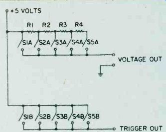
Fig 1. In this version of a simplified voltage keyboard, each switch is a key.
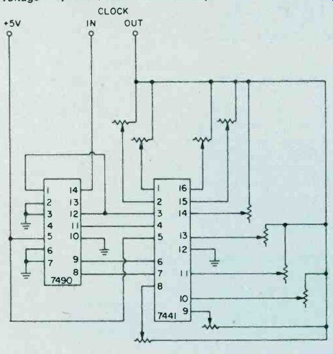
Fig. 2. This simplified schematic of a sequencer utilizes two integrated circuits to order various that in voltages are used producing music. A clock controls the sequence.
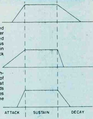
Fig. 3. These three sketches illustrate the range of envelope voltages that be made. The speeds can of attack and decay modes are controlled thru the envelope voltage mode.
The resistor values would be determined experimentally.
The exact voltage doesn't matter so much as the pitch of the VCO, so you'd hook the keyboard to the VCO and try various resistors until it sounds right. You can use fixed resistors connected with spring clips, or potentiometers, which are ore expensive, but give you precise control of the sound.
Sequencers. Another common voltage source is the sequencer. As the name suggests, this device produces a sequence of voltages. For example a sequencer's output might be set to 5V, 4V, 3V, 3.5V, 3V, 2.5V, 3V, 4V. When the sequence reaches its last position, it loops back around and starts over.
A schematic for a simple sequencer is shown in Fig. 2.
Note that the sequencer requires as oscillator to control it. This is not the VOC that produces the signal you hear.
It is a separate oscillator, or clock, that controls the speed of the sequence, consisting of a low frequency squarewave.
As a matter of fact, a spare oscillator can also be used as a varying voltage source. If the controlling oscillator is a very low frequency you can hear its wave-shape (discussed below), but it is in the audible range, very complex tones can be produced.
Function Generators. Another varying voltage source is the function generator or envelope generator. When a function generator receives a trigger signal (such as from a keyboard's second set of switch contacts) its output voltage rises from zero to some specific maximum level (attack). The maximum level is usually held for as long as the trigger voltage is present (sustain). When the key is released, the voltage drops back down to zero (decay). Figure 3 shows some typical envelopes. Figure 4 is the schematic of a simple function generator. Any of these voltages can control a VCO, a VCF, or a VCA, in any combination that you wish to try.
Synthesizing a Flute. For discussing the rest of the synthesizer, let's assume we want to synthesize a flute sound.
We start out with a VCO to produce the original signal.
VCO's may produce any of a number of wave-shapes.
The most common are shown in Figure 5. A sawtooth wave has all of the harmonics. For example, if the frequency of the sawtooth is 100 Hz., then it will also contain tones at 200 Hz. (the second harmonic + 2 x 100), 300 Hz. (3rd harmonic + 3 x 100), 400 Haz. fourth harmonic), 500 Hz. (fifth harmonic), and so forth. The ear automatically combines all of these tones into one raspy sound with an apparent pitch of 100 Hz.
A square-wave, on the other hand, only has odd harmonics. Again, assuming a fundamental frequency of 100 Hz., there will also be tones at 300 Hz. (third harmonic), 500 Hz. (fifth harmonic), 700 Hz. (seventh harmonic), and so on. The resulting sound is rather reedy, vaguely similar to an oboe.
A triangle-wave also contains all the odd harmonic, but they are somewhat weaker than in a square-wave, so the sound is brighter.
A sine-wave has no harmonics, and the sound is very piercing. Actually, it is somewhat unpleasant to listen to by itself, so this waveform is usually only used as a fluctuating voltage source fo control other modules for such effects as tremolo and vibrato.
Filtering. Since the sound of a flute is somewhere in between that of a triangle-wave and a sine-wave, we start out with a triangle-wave, and filter out some of the upper harmonics. (A square-wave could also be used, but more filtering would be required). For this purpose we would use a low-pass filter, which lets low frequencies pass through it, but blocks higher frequencies (i.e., harmonics). For most synthesizer uses low-pass filter is the handiest, but its mirror image; a high-pass filter can also be useful. If you combine these two basic filters as in Figure 8, you have a band-pass or a band-reject filter, so there are a number of effects that can be achieved.
The filters in Figure 7 are fixed filters. That is, their cut-off frequencies are determined by the components values, and remain constant unless the components are changed. This can be troublesome in a synthesizer. Let's say you want a sound with the fundamental, the third and the fifth harmonics only. If we start out with a 1,000 Hz.
signal, the third harmonic is 3,000 Hz., and the fifth is 500 Hz. So we use a low pass filter to lobck everything about 5,500 Hz. Now, suppose we double the frequency and play a 2,000 Hz. note. The third harmonic would be unaffected at 4,000 Hz., but the fifth harmonic would be 6,000 Hz.; which means it would be blocked by the filter.
Or, if we reduce the frequency to 500 Hz., the filter will pass the fundamental (500 Hz.), the third harmonic (1,500.Hz.), the fifth (2,500 Hz.), and also the seventh (3,500 Hz.), and the ninth (4,500 Hz.). Obviously the sound can change quite a bit as the pitch varies.
The solution is to use a VCF, and control it along with the VCO. The patch is shown in Figure 9.
We now have a flute-like sound, but unfortunately, it won't sound very realistic, because each note will instantly be at its maximum level as soon as the key is depressed, and will instantly cut off when the key is released. Real-world sounds aren't like that, and the effect is terribly unnatural. Here is where the function generator and VCA come in. The new patch is shown in Figure 12.
Since the flute is a wind instrument, the sound will take some time to built up to maximum, e the player blows air through the tube. We can simulate this with a fairly slow attack. The sound will also take some time to die out when the player stops blowing, but not as long as it took to build. We'd use a moderate decay time. The envelope voltage applied to the VCA would look like Figure 13.
When no key is depressed, the VCA is cut off. No sound is heard. When a key is depressed, the function generator is triggered. A changing voltage is applied to the VCA. The volume of the signal will vary in step with the voltage.
The noise generating circuit shown in Fig. 14 is a simple but important addition to the synthesizer. It makes for a great deal of flexibility and provides background noise for effect.
At this point we have a fair impression of a flute. Just how good it will sound will depend on the quality of the circuit. Those shown in this article are suitable only for experimentation.
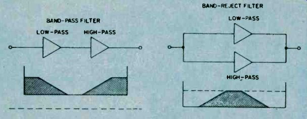
Fig. 8. Combining two filters in parallel or series creates a simple frequency selector.
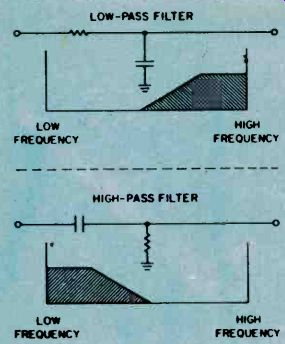
Fig. 7. The arrangement of the Capacitor and the resistor determines cut-off points.
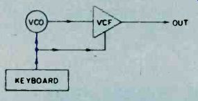
Fig. 9 Using a VCF with a VCO, the proper harmonics of an instrument can be created.
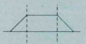
Fig. 10 A low-pass VCF is used to control frequency Enclose photocell and lamp together.
Fig. 11. A simple device, a VGA controls the volume generated so synthesized sound seems real.

Fig 12. This block diagram illustrates how the VCA control fits into the synthesizer.
Fig. 13. The VCA has an envelope voltage, which is shaped like this, applied to it.
Fig. 14. The noise generator of the synthesizer provides background noise for effect.
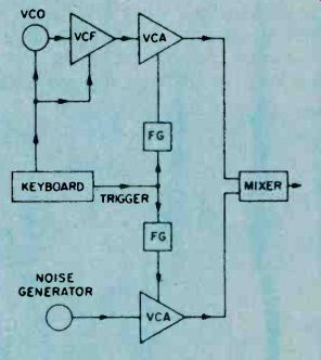
Fig. 15. Adding a little noise to the circuit adds strange qualities to the sound.
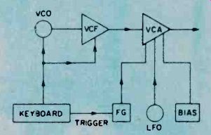
Fig. 16. A variation of the basic patch. which is given in Fig. 15, for the tremolo effect.
We can do a little more to improve realism. For instance, we could add a little noise, as in Figure 15, to simulate the sound of the musician's breath. This noise should have a somewhat faster attack and decay, than the VCO signal, at a much lower level.
We could also add a tremolo (or fluctuating effect) by controlling the VCA with a very low frequency sine wave oscillator (about 5 or 6 Hz.). The bias is a manually adjusted negative voltage that is equal to the peak voltage of the sine wave. This is to cancel out the sine wave when the function generator is not triggered. Thus, the VCA will be cut off between notes.
Synthesizing a Drum. Now that we've synthesized a flute, lets' go back to the patch in Figure 15. Would you believe this is the same patch you would use to produce a drum sound? In this case the level of the noise should be much higher than that of the VCO, and the envelopes would be changed to those of Figure 18A. Figures 18B and 18C show additional envelope settings for unique sounds, not heard in nature. Even with this simple patch, many variations are possible.
Besides changing the envelope, you could change the waveshape of the VCO, or substitute a second FCO for the noise generator, or use high-pass or band-pass filters instead of the low-pass module. You could also use a function generator (or oscillator) to control the filters, or use you imagination.
As you can see, synthesizers really aren't as complex as they seem, yet you can get hours of pleasure out of the simplest collection of modules. Each variation in the way the modules are wired together, will give you a different audio effect. Think of yourself as the conductor who orchestrates the sounds of many musicians. With a synthesizer, you have many more possibilities than with acoustic instruments. The latest trend in music is called New Wave. Its sounds are generated strictly from synthesizers, without any acoustic instruments being used. Eerie sounds seem to echo through distant galaxies, producing strange & hypnotic effects.
======
======
Solar Power Station
By the early 1900's, Israel expects to meet much of its electricity needs with solar generated power. An all solar powered 150 kilowatt generating plant was put into service in late 1979, and more ambitious projects are slated for the future.
The Ein Bokek project, located on the shores of the Dead Sea, makes use of the concept of the solar pond-a body of water whose salt content is such that the water in its depths rises to high temperatures-and a turbo-generator powered by this heat energy. The combination of these two relatively simple and low cost technologies has made possible an innovative approach to electricity production. This large scale application of solar technology is the first of its type.
Solar Priorities. The Israeli government was understandably interested in giving a high priority to the development of solar energy. Continuing hostility from the oil-producing Arab countries dictated energy conservation long before it became necessary for the rest of the world. Israel was one of the first countries to take advantage of the abundant and free energy from the sun; nearly ever rooftop sports a solar water heater, with its distinctive panels and collecting tanks.
A 15,000 square foot solar pond was constructed at Ein Boket by excavating an area of the Dead Sea shore, damming the seaward side, and lining the excavation with a black, heat-absorbing rubber substance. Water was let in, and its salinity level was constantly 'monitored to ensure that the proper gradient level would be reached. The high salt and mineral content prevents normal convective cooling, and the salinity increases with depth. The water at the bottom of the pond rose nearly to boiling temperature after a few hours under the desert sun.
The hot water was then circulated through a heat exchanger, where it heated an inorganic working fluid to the gaseous state. This gas powers a turbine attached to an electric generator.
The turbo generator system that converts the heat of the solar pond into electricity is a unit known as the Ormat Energy Converter (OEC). This is a low-temperature, low-pressure generating system that was originally designed to produce electricity from waste heat. It uses a closed system wherein the working fluid is heated up, used to run a turbine, then condensed and used over again. The OEC is ideal for use in applications where a constant 175-200°F heat flow is available.
Encouraged by the success of the pilot plant at Ein Bokek, the Israeli government has the project's two contractors, Ormat Turbines and Solmat Systems, at work on a 5,000 kilowatt power station. This generating station should be operational by 1981, and will be the first module of a system with an eventual capacity of 2,000 megawatts. Meanwhile, the Rin Bokek plant has been constantly producing 150 kilowatts, day and night, winter and summer. The Dead Sea is a body of water approximately 50 miles long and 11 miles wide: an enormous potential for electricity generation! A Practical Energy Source. Solar ponds occur naturally in many parts of the world, including the U.S., and they can be man-made as well. While the Ein Bokek project was built in an area where temperatures in excess of 100°F are common, the solar pond is equally viable in more temperate climates.
This ambitious Israeli project is just one example of how the dependence on expensive and potentially hazardous energy sources can be offset by solutions developed from Nature.
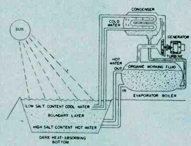
-------This diagram explain the solar pond generating system and shows the transformation of sunlight into electrical energy by taking the heat generated and powering a turbine.
========
=======
Op-Amps How To Use Them
Few linear, (non-digital) integrated circuits (ICs) have achieved the wide popularity of the op amp in hobbyists projects of every description. Combined with few other circuit components, the op amp circuit vastly outperforms the multiple transistor circuit of yesteryear.
Because you will encounter the op amp time and time again in many circuit applications and may desire to work up your own op amp circuits, it is essential to become familiar with the device.
This will introduce you to the basics of op amp circuits and applications. Four simple rules of operation are logically applied to trace and deduce the operation of the basic linear op amp circuits. Test circuits are included for "hands on" familiarity. Only a few mathematical relationships are listed to, effect a comparison of the several circuits.
Some Basics. As shown in Fig. la, the op amp has two input terminals and one output terminal. A plus sign at one input identifies the non-inverting or "follower" input. When this input goes positive (with respect to the other) the output voltage, VOUT, also goes positive, thus "following" the polarity of the input. The minus sign at the other input identifies the inverting input. When this input goes positive (with respect to the other), VOUT goes negative, thus "inverting" the polarity of the input.
In technical terms, the input stage of the op amp is a balanced "differential input' amplifier and is one which responds to the difference between the voltages.
Output voltage VOUT equals VIN times AVOL (AVOL equals the open-loop voltage gain as listed on spec sheets for the op amp used). Input impedance (AC resistance) Z1 and output impedance Soi are shown in Fig. lb. These are the primary characteristics of the op amp. If a perfect op amp could be 'constructed, AVOL and Ai would be infinitely large and Zoi would be zero. Actually, for a general purpose 741 op amp, AVOL equals 200,000, Z1 equal 2 megohms, and Zoi equals 74 ohms.
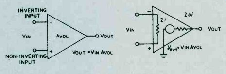
Fig. 1. Two engineering views of a basic op amp. In A, the circuit symbol also provides some insight to what the op amp will do. The circuit model in B should be referred to when investigating circuit design.
Important Concept. In linear applications such as an AC or DC amplifier, the op amp is operated closed-loop with negative feedback. To do this, the loop is "closed" by connecting a feedback circuit from the output terminal to the inverting input; this results in negative feedback. That portion of the output voltage fed back to the input tends to negate, or oppose, the applied input signal voltage. As will be shown later, the resulting closed-loop gain, AvcL, is very much smaller than the open-loop gain. Also, the closed-loop gain now depends on the particular feedback circuit itself and not on the actual value of the open-loop gain. This makes it possible to build amplifiers with precise closed-loop gains.
Among other beneficial effects, negative feedback imparts high linearity and stability to the amplifier.
Rules Of Operation. A few basic facts of op amp operation will be stated as rules and applied to the operation of several circuits. The implications and meanings of these rules will become clear as you apply them to the circuits.
1. The difference in voltage between the + and input terminals is always small and can be assumed to be zero.
(This fact is a direct result of very high AvoL.)
2. The current entering the + and input terminals is small and can be assumed to be zero. (This rule is a direct result of a very high Z1.)
3. If the + input terminal is at ground voltage or zero, the ‘-’ input terminal can be assumed to be virtually at ground voltage or zero. (This rule is also a direct result of high AvoL.)
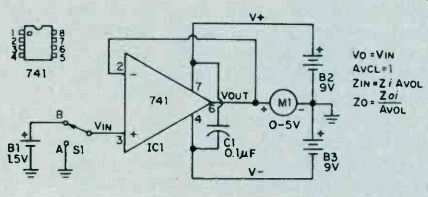
Fig. 2. Here an op amp is hooked up to provide unity gain.
The output voltage equals the input voltage due to the feedback of the non-inverted output of the op amp to the inverting input effectively reducing the gain of the stage to 1.
4. When an op amp is connected in a negative feedback configuration, a voltage change at the + input must result in an equal voltage change at the ‘-‘ input terminal. (This is a description of rule 1 in operation.)
Setting Up. Breadboard the op amp circuit shown in Fig. 2. You can use perforated board and flea clips to assemble the circuit. Better still, use a solderless breadboard kit. Use only the 741 op amp for IC1. These are short-circuit proof and are internally frequency compensated to prevent oscillations. Switch S1 may be simulated by a clip lead.
Install disc capacitor C1 as close as possible to the IC. Use either a common tie point for all ground connections or a heavy ground bus. Keep the input lead wires well separated from the output lead wires. The prototype breadboard uses a 50 uA DC meter connected in series with a 100,000-ohm, 1% resistor for meter M1.
Alternately, you can use your VOM (1000 ohms/volt or better) to measure output voltage. Use two fresh nine-volt transistor batteries for B2 and B3 and 1!i volts (an AA cell) for BL
Unity Gain Follower. Simplest of the op amp circuits, the unity-gain follower shown in Fig. 2 has a direct connection from output to the inverting input.
This provides one-hundred percent negative feedback.
With switch Si at position A, the + input is grounded and meter Ml indicates zero. By rule 3, the ‘-’ input is at virtual ground. Therefore, VOUT is also at virtual ground. With Si set to position B, the meter now indicates the voltage of battery B 1, near 1.5 volts. By rule 4, the 1.5 volt increase at the + input must be accompanied by a 1.5 volt increase at the ‘-‘ input.
Hence, VOUT must rise to 1.5 volts.
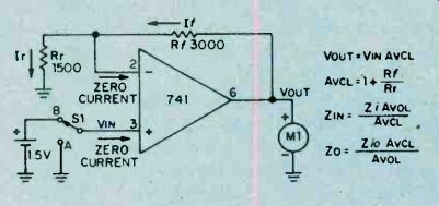
Fig. 3. With the feedback signal reduced, the gain of this op amp non-inverting
voltage amplifier is 3. The meter should read 4.5 volts with 1.5-volt
input.
The resulting closed-loop gain, or AvcL, is unity (one unit out for one unit in). However, the high AvoL inside the IC itself is still present, enforcing close compliance with the several rules. As noted on Fig. 2, actual input and output resistances ZIN and Zo are much improved due to feedback. The resultant input resistance now equals Zi times AVOL or400,000 megohms for the741 op amp! The resultant output resistance now equals Zoi divided by AVOL, or .0035 ohms! Consequently, the unity gain follower can duplicate the input voltage at its output without loading down the input voltage source due to the high input resistance and with high accuracy due to the low output resistance. Actually, input and output resistances are degraded somewhat by secondary factors. Nevertheless, this unity gain follower offers the highest input resistance and lowest output resistance of the several basic circuits.
Non-Inverting Voltage Amplifier. Stable op amp voltage amplification is obtained by feeding back only a portion of the output voltage. Alter your breadboard circuit to include feedback voltage divider resistors Rf and Rr, as shown in Fig. 3. With Rf equal to 2Rr,,only one-third of the output voltage is fed back to the inverting input. 1 With Si at position A, the + input is at ground voltage and the meter indicates zero. By rule 3, the ‘-‘ input is at virtual ground or zero. With zero voltage across Rr, current Ir is zero. In view of rule 2, If always equals Ir and is zero in this case. With zero current in Rf, the ‘-‘ input and the output voltage must be equal and zero in this instance.
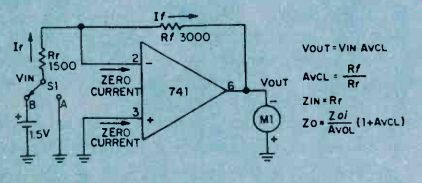
Fig. 4. The circuit arrangement of the op amp provides an inverting output with a gain of 3. Compare it to fig. 3.
With S1 at position B, the + input is raised 1.5 volts and the meter indicates 4.5 volts. By rule 4, the ‘-’ input must rise to 1.5 volts matching that at the + input. The op amp does this by forcing a current into the feedback voltage divider as shown. With 1.5 volts across Rr, current Ir equals 1.5 volts divided by 1500 ohms, or 1 mA. Also, the voltage across Rf equals 1 mA times 3000 ohms or 3 volts.
Thus, VOUT equals 1.5 plus 3 or 4.5 volts.
Closed-loop voltage gain AVCL equals 1 + (Rf/Rr) or 3 in this case. Compared with the unity gain circuit, actual output resistance Zo is three times grater and input resistance ZIN is one third that of the unity gain circuit.
This reflects the effect of feeding back 1/3 of the output voltage. To obtain a closed-loop gain of ten, resistor Rf must equal 9Rr, and so forth.
Inverting Voltage Amplifier. Alter the breadboard circuit to that of Fig. 4 including reversal of the meter.
With S1 at position A, the meter indicates zero. The proof of this result is identical to that of the non-inverting voltage amplifier with switch at position A. With S1 at position B, the meter indicates 3 volts (actually, minus 3 volts since the meter is now reversed).
In this case, the ‘-’ input does not rise to 1.5 volts. By rule 3, with + input grounded, the ‘-’ input must remain at virtual ground. Therefore, and quite importantly, the voltage across Rr equals the input voltage, or 1.5 volts divided by 1500 ohms, or 1 mA, flowing in the direction shown. Since If equals 1 mA times 3000 ohms, or 3 volts.
With the ‘-’ input at virtual ground, the output voltage must be minus 3 volts as indicated on the reversed meter.
The closed loop voltage again, AVCL, is simply Rf/Rr, or 2 in this case. Quite unlike the previous cases, actual input resistance ZIN equals Rr, the input resistor.
Compared with the unity gain non-inverting amplifier, actual output resistance Zo is greater by a factor of (1 + AvcL) or three times as much, still acceptable small at this (and even much higher) gain.
By connecting additional input resistors to the ‘-’ input and upon applying several input voltages, the amplifier will sum the several input voltages at the output. For this reason, the amplifier is often termed a summing amplifier and the ‘-’ input is termed the summing node or input.
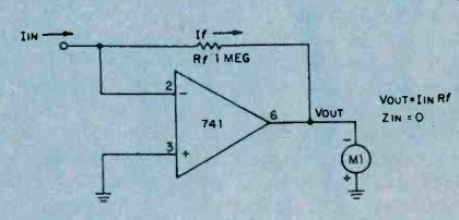
Fig. 5. Using only one external circuit element, this op amp functions as a current-to-voltage converter.
Current to Voltage Converter. A variation of the inverting amplifier, the current to voltage converter shown in Fig. 5, omits input resistor Rr. Because the ‘-’ input must remain at virtual ground for linear operation, this circuit cannot accept an input voltage. Instead, it accepts an input current and is used to measure very small currents. If IIN were 1 micro A, the output voltage would be 1 micro A times 1 megohm, or 1 volt. By making Rf very large, the circuit can measure extremely small currents. The input resistance of this circuit is zero. The output voltage, VOUT, equals IIN times Rf.
If you breadboard this circuit, you may observe a small output voltage at zero input current. This output "offset" voltage is caused by the flow of a small bias current from output to input through the large feedback resistor, Rf. Unless special opamps having very low bias currents are used, it is necessary to include a nulling circuit to reset.
Input Bias and Offset. Although rule 2 assumed zero input currents, an op amp does require a small input current Ib to bias the input stage into linear operation.
For the 741, Ib may range up to 0.5 uA. The difference between the input bias currents at the two inputs is the input offest bias current ziio. This current is usually much smaller than Ib. Both Ib and Iio cause an objectionable output offset voltage with Rf is very large. To restore the output voltage to zero, add the nulling circuit potentiometer R1 and resistor R2 as shown in Fig. 6. With Si open, adjust the control until meter indicates zero.
If Rr is small, and upon closing S1, you may observe that the meter again loses its zero. This is caused by the input offset voltage Vio resulting from slight mismatches of the input transistors. Input offset voltage Vio is defined as that input voltage required to restore VOUT to ,zero. It is measured under open-loop conditions with very low value resistors at the input. For the 741, Vio may range up to 6 millivolts. Conveniently, the 741 includes terminals allowing compensation for input offset voltage. Add potentiometer R3 and adjust the control with Si closed, until the meter indicates zero. If both circuits are included, adjust the controls several times in succession.
Conclusion. Having become acquainted with the basic operation of the op amp, and with some knowledge of the six primary op. amp specifications, you will now be able to experiment with op amp circuits with some degree of confidence rather than apprehension. With some appreciation of how and why the circuit functions as it does, how the performance of the several circuits compare with each other, and how negative feedback plays its pact, you will find that op amp literature and circuits are more easily understood.
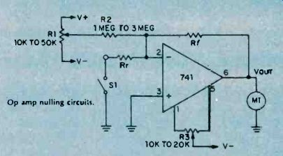
Fig. 6. When required an offset voltage can be added to the op amp circuit.
========
=======
Amplifiers that Oscillate
As any slightly cynical experimenter can tell you, if you want an oscillator, build an amplifier-it's sure to oscillate. Conversely, if you want an amplifier, (this same cynic will tell you), build an oscillator--it's sure to fail to oscillate, and you can then use it as an amplifier! This is well known as a corollary to Murphy's famous law, "If anything can go wrong-it will!" Our informed cynic must have had long and unhappy experience with negative-feedback amplifiers, which are known to have at least two outstanding characteristics:
1. They function beautifully if carefully designed and built.
2. Otherwise, they oscillate!
Why do they oscillate? Or, more basically, how does a feedback amplifier differ from an oscillator? The fundamental block diagrams of an oscillator and an amplifier with feedback bear a strong resemblance to each other, as you can see from Fig. 1. From a block diagram viewpoint, both diagrams are very similar. Both contain some type of amplifying device, and both have part of their output signal fed back to their input. There are only two major differences between them:
1. The amplifier with feedback contains an inverting amplifier; the oscillator contains a non-inverting amplifier.
2. The oscillator doesn't have an input.
The circuit action obtained from these two circuits is entirely different. In the amplifier with feedback, the output waveform is upside down with respect to the input, so when it is fed back to the amplifier input, it cancels a portion of the input waveform. The output is therefore less than it would Be-without feedback. See Fig. 2.
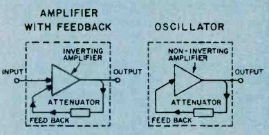
Fig. 1. Two block diagrams compare an inverting amplifier (A) to an oscillator (B).
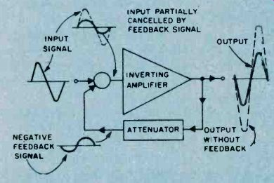
Fig. 2. Signal flow diagram illustrates how feedback in an inverting amplifier circuit reduces overall gain.
The feedback signals from inverting amplifiers are not "in phase" with the input signal and subtract (or reduce) the input signal level to the amplifier. When a feedback signal does this, it is called negative feedback.
So Why Negative Feedback?
Of course, if you merely want the biggest possible gain for your money, negative feedback's not your game. However, negative feedback offers other advantages, which can be summed up by saying that the amplifier's output, though smaller, is always nearly constant for the same input signal. For example, if the amplifier weakens with age, and the output tries-to drop, there is less signal to fed back; hence there is less cancellation, and the output is restored almost to its former level. Similarly, if you feed a high frequency signal through the amplifier-so high in frequency that the amplifier can barely amplify it-the resultant drop in output reduces the fed-back voltage, produces almost no cancelling feedback signal, and keeps the output nearly the same as it was at lower frequencies. Moreover, any clipping or other distortion of the waveform inside the amplifier produces an output waveform which does not match the input; hence the non-matching part is not cancelled, and the distortion is removed, or at least greatly reduced. Without this action, hi-fi amplifiers would not exist.
So the loss in output you obtain from negative feedback repays you by providing less distortion, better long-term stability, and better frequency response-that is, the best and most uniform output in response to all input frequencies.
On the Flip Side. The oscillator, on the other hand, is not supposed to give the best output from all input frequencies, but is instead made to give an output at a single frequency-with no input at all. It's not surprising that the opposite type of internal amplifier (non inverting) is used to obtain this opposite result. See Fig. 3.
In the oscillator, any output at all (probably the result of some random noise in the internal amplifying device) is fed back, non-inverted, to the input, where it does not cancel but instead serves as the signal at the input. This feedback signal causes an even larger output, which results in an even larger signal fed back, further reinforcing the input signal, and so on.
You guessed it-this type of feedback signal is commonly referred to as positive feedback. In theory, the output waveform should continue to get larger forever. In practice, the amplifier is limited in the maximum size of the signal it can deliver, so the output waveform stops growing in this amplitude. As it stops to grow, so does the positive feedback signal. Now the signal reduces rapidly and the positive feedback signal lends a hand until the signal can get no lower. This is the beginning of the first cycle of many to follow.
All well and good, you say, but if the major difference between feedback amplifiers and oscillators is the inverting or non-inverting nature of their internal amplifiers, why does an amplifier sometimes oscillate? What turns an inverting amplifier into a non-inverting one? To answer this question, first observe that an inverting amplifier, in passing a sine-wave signal, effectively shifts the signal's phase by 180° as shown in Fig. 4. We say effectively, because it doesn't really shift the timing by delaying the signal (which is what a real phase-shifter does) but, by turning the signal upside down, the amplifier makes it look like a signal which has been delayed (phase-shifted) by 180°. A real phase-shifter, on the other hand, is normally nothing but a fistful of judiciously connected resistors and capacitors (and sometimes inductors) which can be designed to give a 180° phase shift at a single frequency, such as 1,000 Hz, for example. In contrast to an inverting amplifier, it provides this phase shift by actually delaying the signal. See Fig. 5.
What happens if we combine an inverting amplifier and a 180° phase-shifter? Take a look 'at Fig. 6.
This combination will shift the phase of a given frequency by a total of 360° (an entire cycle) so the output is identical to the input. In effect, this combination (at 1,000 Hz) will behave the same as a non inverting amplifier. See Fig. 6.
Therefore, if we build a feedback amplifier which contains the normal inverting amplifier but also (inadvertently) contains a 180° phase-shift network, the resultant circuit will oscillate at the particular frequency, (1,000 Hz in the figure) for which the phase-shifter provides 180° phase shift. See Fig. 7.
How can one "inadvertently" make a phase-shifter? It's easier than you might think. The circuit shown in Fig. 8A will provide 60° phase shift at 1,000 Hz. Three such networks connected in a "ladder" (see Fig. 8B) will proved 3 x 60° = 180° of phase shift. (But not at 1,000 Hz. Because of the way the networks load each other, the 180° shift occurs at 707 Hz. However, if an amplifier were located between each network, then the amplifier will oscillate at 1,000 Hz.) This network, if dropped into a normal feedback amplifier circuit, will convert it to an oscillator.
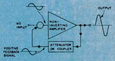
Fig. 3. Signal flow diagram shows how feedback signal from a non-inverting amplifier provides the positive feedback to produce an output signal larger than it would otherwise be without feedback.
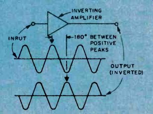
Fig. 4. The apparent phase shift of the output signal from the input signal is 180 degrees.
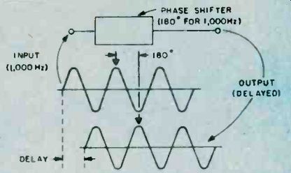
Fig. 5. The passive phase-shift circuit actually delays the output signal by a time interval measured in degrees by that portion of a sine wave so delayed. This effect appears to the apparent delay of an inverting amplifier.
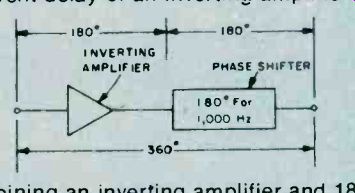
Fig. 6. Combining an inverting amplifier and 180 degree phase-shift circuit results in a 360-degree phase shift at 1000 Hertz only, which results in a non-inverting amplifier circuit.
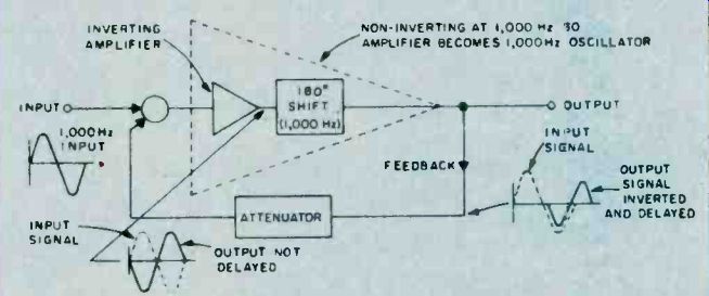
Fig. 7. Since the 180-degree phase shift is frequency selective, this non-inverting amplifier will oscillate at 1000 Hertz.
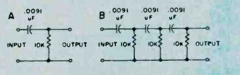
Fig. 8. In this diagram, a simple network (A) offers 60 degrees of phase shift at 1000 Hertz. Ladder three such circuits in series and the total phase shift at 1000 Hertz will be 180 degrees.
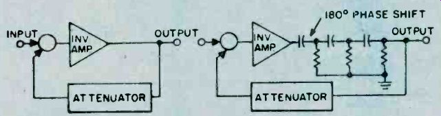
Fig. 9. Two inverter amplifiers are shown here with one having a 180-degree phase-shift network added to induce positive feedback. The RC elements limit this oscillation to be a fixed frequency.
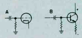
Fig. 10. External parts in this amplifier circuit have the same effect as the phase-shift circuit in Fig. 8A. However, values for the resistance and capacitance are selected to produce almost no phase-shift within the amplifiers normal frequency bandpass.
This circuit (Fig. 9) is known as a phase-shift oscillator and is widely used in electronics.
Of course, when you set out to build a phase-shift oscillator, you deliberately insert a phase-shifter to make the circuit oscillate. How could one ever inadvertently place such a circuit in a feedback amplifier, thereby producing unwanted oscillations? Phase-shift circuits can "hide" within an amplifier, posing as other circuits. For example, vacuum-type amplifiers often have grid circuits arranged as shown in Fig. 10A. Does that resistor/capacitor circuit look familiar? In form, it's just like the phase-shift circuit above. And transistor amplifier circuits often take the form shown in Fig. 10B. Again, the coupling/biasing network looks just like the basic phase-shifter network. At some frequency, this network will provide 60° of phase shift. If we use three such identical networks in a three-stage amplifier w.e have a 180° phase-shift network "buried" inside the amplifier, masquerading as three normal coupling networks. If this three-stage amplifier is used as part of a feedback amplifier arrangement, the amplifier will oscillate at some frequency, and be quite useless for the purpose for which it was intended.
More Trouble. This is not the only way an amplifier can get into trouble. There are other types of phase shifters that can creep into amplifiers, unrecognized, and drive the unwary experimenter up the nearest wall. This circuit (shown in Fig. 11A) can also produce a phase-shift of 60° at 1,000 Hz. Three of them, can produce the 180° phase-shift required for oscillation. See Fig. 11B. This particular network can invade amplifiers in an even more insidious fashion. The "masquerading" part of the circuit is shown heavy in Fig 11C. The dotted capacitor doesn't appear physically in the circuit, because it is the so-called "stray capacity" associated with wires, sockets, terminals, etc. Three of these circuits hiding in an amplifier, can produce an unwanted oscillation. See Fig. 12. Since the stray capacities are so small, this "osc-plifier" will oscillate at a very high frequency; often so high that it is undetected as an oscillation. However, such oscillation can make an amplifier behave erratically; sometimes distorting, sometimes not; sometimes overheating, sometimes not. Fig. 7 and Fig. 12 have a lot in common.
Are feedback amplifiers the only culprits in this oscillating-amplifier business? Absolutely not! Often, so-called "straight" amplifiers--with no intentional feedback-will gaily oscillate away. But watch that word intentional. Close inspection of these misbehaving circuits usually uncovers an unintentional feedback path hiding within the amplifier. Consider the innocent looking circuit in Fig. 13. This is an ordinary two-stage amplifier, obviously assigned the task of converting a small, positive-going signal into a large, positive-going signal. To help it along, the designer has even provided a decoupling network, R1 and C1. At high frequencies, C1 acts like a short circuit, effectively isolating (de coupling) the amplifier's power bus, Ecc +, from the main power bus, Ecc + +. But, at low frequencies, the capacitor acts like an open circuit-it just isn't there! A small part of the output voltage now appears across R1, and is coupled through the amplifier's power bus back to the input, arriving there with the same polarity as the normal input. True, the signal unintentionally fed back isn't very large, because the unintentional feedback path provides substantial losses for this stray signal. For example, the signal may arrive back at the input 100 times smaller than it was at the output. However, if the amplifier has a gain of 101, it makes an even larger output signal out of the fed-back signal, which then is fed back as, an even larger voltage and oscillation begins.
Careless construction can get you into trouble, too.
The amplifier shown in Fig. 14 is trying to convert a 10 millivolt input into a 200-ma signal needed by the load, R2. The builder has tied all ground returns to a heavy ground bus, and returned this bus to ground at only one point. Unfortunately, that single ground wire has to carry both the tiny input signal and the large output current.
And, since every wire has some resistance, the actual circuit includes an 0.06-ohm resistor that does not appear in the original construction schematic diagram, but must be considered and is shown in Fig. 14.
Again, an uninvited, unintended feedback path has appeared, coupling the output back to the input. In the sketch, the large output current, flowing through the tiny ground-lead resistance, produces a voltage which is even larger than the original input voltage. And, since this voltage is also connected to the input (through the bias resistor R3), the fed-back voltage appears un-inverted (and uninvited!) at the input, and will cause the amplifier to oscillate. What is to be done to convert these oscillators back into well-behaved amplifiers? The general rule is divide and conquer. In the example just above, we can conquer the oscillation by dividing the ground returns, making sure that the high-current output circuits and the sensitive input circuits have their own private and individual paths to the power supply.
See Fig. 15.
Short leads to the input connector are also helpful in squashing oscillations.
The misbehaving decoupling network, R1 and C2 in Fig. 13, can also be brought under control by dividing the network into two decoupling networks as shown in Fig. 16.
The stray capacities causing the unwelcome phase shifter to hide in the best divide-and-conquer approach to this amplifier are harder to exorcise. Your amplifier is to put feedback around only a pair of stages instead of three or more. This way, there are only two pairs of stray Rs and Cs lurking in the amplifier, and it takes at least three such pairs to make an oscillator.
The coupling capacitors, which combined to make a phase shifter in the very first example, can be prevented from ganging up on the amplifier and making it oscillate by making the product of each capacitor times its associated resistor (called the "RC product") 5 or 10 times larger or smaller than the other RC products. For example, in a three-stage feedback amplifier which has all its base resistors the same values, you could make the three coupling capacitors 2 uF, and 10 uF, and 60 uF, respectively. Again, you have divided the coupling capacitors into three widely-separated values, and conquered the oscillation.
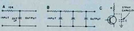
Fig. 11. Don't get confused with the circuit elements shown in (A) with those shown in Fig. 8A. The reversal of parts converts the basic circuit from a coupler to a filter with the attending phase shift. Three series-connected filters have the same effect (B) by providing 180-degree phase shift.
Hidden capacitance (C) internal to the circuit element and in the external wiring will provide some phase shift of the output signal in this amplifier.
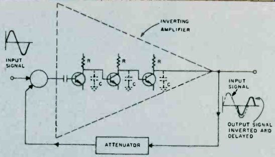
Fig. 12. An inverting amplifier may oscillate do to stray capacitance in these external circuit amplifiers providing a 180-degree phase shift at some very high frequency.
Output signal is within frequency bandpass of the amplifier before phase shift causes oscillation (positive feedback).
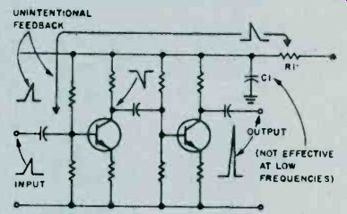
Fig. 13. Low frequency feedback occurs because the capacitor C1 is not effective at these low frequencies.
Thus, any portion of the output signal that will cause a ripple in the power supply will serve as a positive feedback.
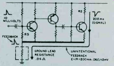
Fig. 14. A ground bus has a finite resistance, and, when high-current output signals mix with low-level signals in the same bus, positive feedback may result with the attending possibility of oscillation.
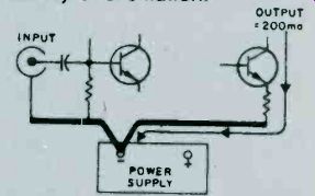
Fig. 15. Divide and conquer-separate input connections from output connections to different buses, and a good deal of the unwanted signal mixing will not occur. The resistance of the power supply must be very low otherwise all that is gained using this construction technique will be lost.
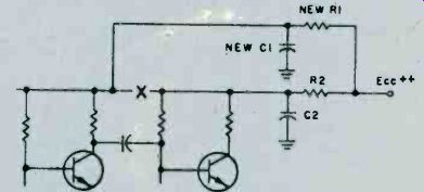
Fig. 16. A good idea is to split up the voltage distribution to many circuit points by two or more power supply decoupling networks. Compare this diagram to Fig. 13.
=====
=====
Am/Fm Receiver Alignment
The words "receiver alignment" often conjure up a mysterious and complicated procedure which can be performed only by an expert. While it is true that receiver alignment should not be attempted by anyone who does not have the necessary skills and equipment, it is not a very difficult procedure if you have some basic guidelines. This article will explain the various procedures for aligning AM, FM, and AM/FM receivers using a minimum of equipment.
Before getting into the mechanics of receiver alignment, it is important that the service technicians understand the basic operation of the receiver, and why proper alignment is necessary. To this end, a discussion of the modern superheterodyne receiver will follow.
Receiver Fundamentals. Virtually every AM and FM receiver manufactured today is a superheterodyne receiver. They utilize a built-in RF oscillator and mixer circuit to convert the received signal to a lower frequency called an intermediate frequency (IF). In a given AM or FM receiver, the IF remains the same frequency regardless of which radio station is being received.
The basic advantage of this type of circuit is that the greatest part of the RF gain, and bandpass characteristic of the receiver, is provided by the IF stages, and is a constant for all received frequencies. Thus, the manufacturer of the receiver can precisely determine the sensitivity and selectivity of the receiver. Proper alignment ensures that the receiver performs exactly the way the manufacturer intended. Refer to Fig. 1, which is a simplified schematic diagram of the RF and IF sections of a typical modern day AM receiver.
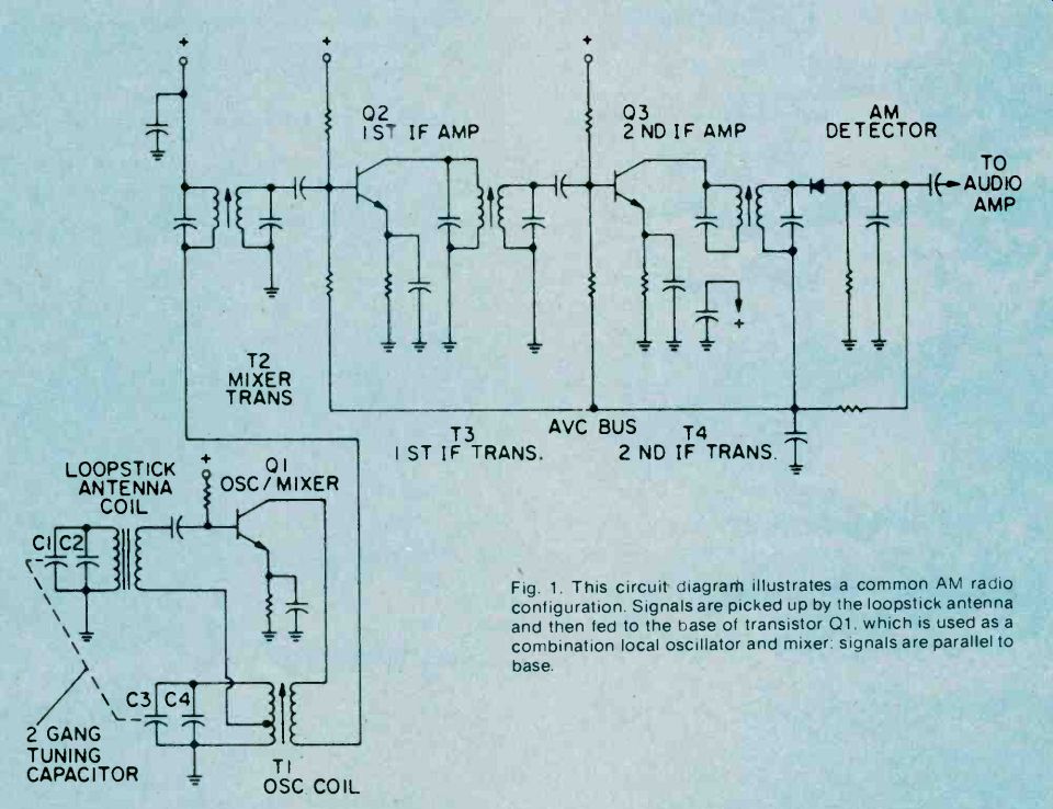
Fig. 1. This circuit diagram illustrates a common AM radio configuration. Signals are picked up by the loopstick antenna and then fed to the base of transistor 01. which is used as a combination local oscillator and mixer: signals are parallel to base.
In Fig. 1., simplified AM radio schematic, you will note a combination mixer-oscillator stage, and two stages of IF amplification. This circuit is typical of a minimum cost AM receiver which has a two gang tuning capacitor and no FR amplifier. Such a circuit might be used in a common pocket-sized AM transistor radio.
More expensive receivers will use a similar circuit with the addition of a transistor stage for RF amplification.
In the circuit of Fig. 1, the received signals is picked up by the loopstick antenna and is fed to the base of Ql. This transistor stage is used as a combination local oscillator and mixer, and is actually a Hartly oscillator with the received signal being placed in series with the base drive of the oscillator. The frequency, of oscillation is determined by>C3, C4 and T1. At the same tithe C1, C2 and the loopstick antenna are tuned to the received signal frequency. The output of T2 contains several frequencies: the radio station frequency, the local oscillator frequency and two new frequencies equal to the sum and difference of the local oscillator and received frequency.
It is the function of the two IF stages, Q2 and Q3, to amplify the difference frequency (IF) and reject all others. This is accomplished by tuning all IF transformers, T2, T3, and T4, to the specified frequency.
For most ANI receivers, this is 455 KHz. The tuning of these transformers is performed during alignment of the receiver.
FM Circuitry. Fig.2, is a simplified schematic of a typical FNI receiver. In this diagram you will note the similarity with the AM receiver schematic of Fig. 1. This basic difference, aside from the higher operating frequency, is that the FM receiver employs an RF amplifier stage, Ql.
Most FM receivers have at least one RF amplifier, since it is the nature of FM transmission that weaker signals than AM are usually encountered. Good FN! reception requires a solid signal in the IF amplifier, so that effective limiting takes place. Note also the requirement of a three gang variable capacitor instead of the two gang as appears in Fig. 1. The additional cost and size of this capacitor is one reason why most AM receivers have no RF amplifier stage.
Although the IF amplifier stages of the AM receiver and FM receiver appear to be similar, there is a substantial difference in the way in which they are designed. The bandwidth of an AM radio station is just 10 KHz, and the receiver must be designed to have an IF bandwidth no greater than this. Such a narrow bandwidth is easily co trolled by the design of the IF transformers which, when turned to the same frequency such as 455 KHz, will provide the desired bandwidth of 10 KHz.
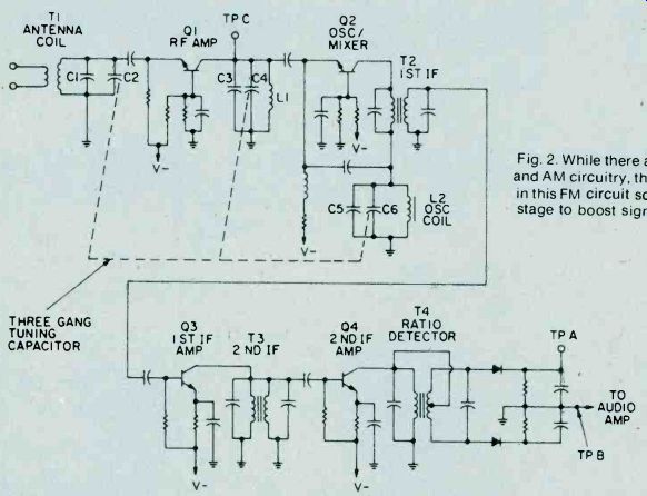
Fig. 2. While there are similarities between FM and AM circuitry, the most obvious difference shown in this FM circuit schematic is an RF amplifier stage to boost signals.
In the case of FM reception, and especially Stereo Multiplex FM, good reception requires a receiver with at least 150 KHz bandwidth. It is the nature of FM to have significant sidebands on either side of the carrier frequency, as far away as 75 KHz. Such a wide bandwidth in the IF stages of an FM receiver cannot be attained by tuning each stage to the same frequency.
What is done is to stagger tune each stage, so that the resultant overall response has the required bandwidth.
Note that each IF transformer in Fig. 2 has separate tuning slugs for primary and secondary which permit stagger tuned alignment.
Because of the problem of attaining proper alignment in the IF stages of an FM receiver, the more expensive designs utilize special filter circuits which are tuned to the factory and require no adjustments in the field. You will find that many modern stereo receivers are designed this way. However, these types of receivers still require alignment of the RF and local oscillator sections of the unit as you would expect.
AM Receiver Alignment. Alignment of an AM receiver is a relatively simple procedure, and can actually be performed by using existing radio stations as a signal source instead of a signal generator. However, if a signal generator is available, it is always best to use it as described in the following paragraphs.
When performing the alignment of an AM receiver, connect a few loops of wire across the output cable of the signal generator and loosely couple the loops to the AM antenna coil. Use the smallest RF output from the generator that will produce a reliable meter reading. For a tuning indicator you can connect a VTVM or VOM set to measure AC volts across the voice coil of the speaker.
An alternate method is to measure the DC voltage level on the AVA (Automatic Volume Control) line of the receiver. This requires a high impedance DC voltmeter such as a VTVM. The alignment procedure will, of course, depend upon the number and type of adjustments in the specific receiver under test. If possible, obtain the manufacturer's alignment procedure. In the absence of such information you can use the following procedure.
IF Alignment. The first adjustment to be performed is the IF alignment. Set the signal generator at 455 KHz, with about 30% to 90% amplitude modulation. Loosely couple the output of the generator to the antenna coil of the receiver and listen for the audio modulation in the receiver speaker as the RF generator is varied about 455 KHz. If you do not obtain any audio around this frequency, the IF of the receiver may be another frequency, such as 262 KHz.
Once you have determined the proper frequency, set the generator at 455 KHz. or whatever the specified intermediate frequency may be. Connect the VOM across the voice coil of the receiver and adjust the IF transformers (T2, T3, and T4 in Fig. 1) for the maximum reading of the meter.
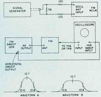
Fig. 3. A matching circuit must be used when attaching sweep generators to FM sets.
Fig. 4. When using both a sweep generator and oscilloscope for aligning an FM set, they must be connected in the manner shown in the diagram on the right side.

Fig. 5. The lower-quality FM receivers will have a waveform resembling A; while better sets will show something more like B.
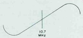
Fig. 6. Adjust the secondary of the discriminator transformer 'til it centers 10.7 MHz.
As you progress with the IF alignment, you may find that you can lower the RF output of the signal generator to prevent overload of the receiver. When you are satisfied that all IF transformers are tuned so that no further increase in meter reading can be attained, the IF alignment is complete.
The next set of adjustments will align the upper and lower settings of the tuning capacitor. This is accomplished in two steps, which will have to be repeated several times, since the adjustments have some interaction with each other.
The initial adjustments are made at the high end of the broadcast band. Set the tuning dial to a silent point (where no radio station is received) near 1600 KHz. Set the RF signal generator to the same frequency. Adjust the two timer capacitor (C2 and C4 in Fig. 1) for maximum meter reading.
Then set the tuning dial of the receiver to a silent point around 600 KHz. and set the signal generator to the same frequency. Adjust the oscillator tuning coil (T1 in Fig. 1) for maximum meter reading.
Repeat the adjustments for 1600 KHz and 600 KHz as described above until no further improvement can be made. Once you have done this, the AM alignment will be completed.
FM Receiver Alignment. Proper FM alignment requires the use of a sweep generator and oscilloscope, unless the receiver under test has a fixed tuned IF section which is permanently aligned at the factory. The generator may be coupled to the antenna terminals of the receiver using the circuit of Fig. 3, which matches the 50-ohm impedance of the generator to the 300-ohm input impedance of the FM receiver.
Some receivers may have highly selective front ends which make injection of the 10.7 MHz IF through the RF stages difficult. In these receivers you may couple the output of the signal generator to the input of the first IF amplifier stage through a 10-pf capacitor. This point is shown in Fig. 2, as test point C. Use only sufficient signal strength to achieve a usable display on the oscilloscope.
Fig. 4, is a typical connection diagram of the receiver, generator and oscilloscope.
The first section of the FM receiver to be aligned is the IF amplifier. Set the signal generator to a center frequency of 10.7 MHz. and a sweep width of about 450 KHz. An FM sweep generator should have a marker system which allows you to identify the important frequencies of interest, such as 10.6, 10.7, and 10.8 MHz.
These markers indicate the desired bandwidth of the IF amplifier.
Connect the Y input of the oscilloscope to test point A of Fig. 2, and adjust the scope controls to obtain a display similar to Fig. 5. Adjust all IF transformers (T2, T3, & T4 in Fig. 2) so that the amplitude of the display is maximum, while preserving the symmetry of the waveshape at about 10.7 MHz. Bear in mind that low cost FM receivers will have a waveshape similar to that of waveform A, while high quality receivers will have the preferred waveshape B of Fig. 5.
The next step is the adjustment of the Ratio Detector or Discriminator. Connect the Y input of the oscilloscope to test point B of Fig. 2, and adjust the secondary of the Ratio Detector or Discriminator transformer (T4 of Fig. 2) to place the 10.7 MHz marker at the center of the S curve, as shown in Fig. 6. Readjust the primary of the same transformer for maximum amplitude and straightness of the line between the positive and negative peaks. This completes the alignment of the IF section of the receiver.
Trimmer. Adjustments. The final adjustments to the FM "receiver are made to the trimmer capacitors, which are connected in parallel with the main FM variable capacitors. These are shown in Fig. 2 as C1, C3 and C5.
Note that some FM receivers, especially the higher quality ones, may have four such trimmer capacitors.
These adjustments are made with the FM tuning dial set to near the high end of the range, (108 MHz). Set the FM dial to a silent point near 108 MHz. Set the signal generator to the same frequency as the dial setting, and couple the output of the generator to the antenna terminals of the receiver as shown in Fig. 3. Connect a DC voltmeter to test point A as shown in Fig. 2, and use only enough signal output from the generator to attain a reliable meter reading. Adjust C1, C3, and C5 as shown in Fig. 2, for maximum meter reading.
As a final check, set the receiver dial to a silent point, near the low end of the range, 88 MHz, and set the generator frequency to the same frequency. Now, by varying the generator about 88 MHz while watching the DC voltmeter, you can determine how accurate the FM dial is.
Keep in mind that if you do make this adjustment you will have to go back to 108 MHz and readjust the trimmer capacitors again. In addition, if you are working on an AM/FM receiver slipping the dial pointer will also require a realignment of the RF section of the AM receiver. For. these reasons it is not recommended that the dial be slipped unless it already has been placed far out of calibration through some previous servicing procedure.
========
========
Signal Propagation
The propagation of all radio waves may be defined as: "The traveling of wave energy through the atmosphere." How do signals get from one side of the world to the other? The ionosphere, a region of the earth's atmosphere extending upwards from 50 to 350 miles (80-560 kilometers), has ionized layers with the ability to reflect electromagnetic energy of certain frequencies.
The purpose of this article is to review, briefly, the components of the ionosphere, some propagation characteristics, and some ways that you can tell whether or not the amateur bands are in good condition for DX communications.
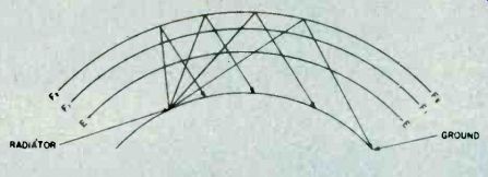
Fig. 1. The diagram above shows the effects of interaction between three layers on the reflection of radio waves back to Earth receivers.
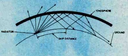
Fig. 2. This diagram demonstrates the principle of skip.
You can see effects of ionospheric reflection of radio waves.
The Ionosphere. In 1901, Marconi succeed in transmitting radio signals from England to America, over the bulge of the earth. Since it was known that electromagnetic waves travel in straight lines, Heaviside and Kennelly proposed in 1902 that the radio waves had been reflected from an atmospheric layer consisting of , free electric charges. Heaviside called it the "electrified layer", and others called it the "Heaviside layer." Later, Appleton discovered between the two layers, and to make room for other possible layers, he called the Heaviside layer the E layer, and the new layer the F layer. Subsequently a lower layer was discovered, called the D layer. It was also found that the F layer consisted of two layers which separated during the day and merged at night, and the concentration of electrons decreased in all layers at night.
The D-layer (50 miles or 80 km up) assembles during the day and disappears at night. It primarily affects 160 to 180 meters, limiting daytime coverage to ground-wave by absorbing sky-wave signals.
The E-layer (75 to 120 km up) provides stable sky-wave coverage during the day on 10 through 40 meters, and on 80 to 160 at night. The nominal skip distance is around 1,000 miles (1,600 km), but double hops can and do occur. During primarily the summer months, sporadic-E-extra-thick patchy clouds of ionization--opens 6 and 10 meters for short duration openings during the day or night.
The F-layer at night is about 200 miles (320 km) high, and during the day, it separates into the Fi-layer (125 miles or 200 km up), and the F2-layer (250 miles or 400 km up). These layers are the mainstays of the DX'ers looking for worldwide coverage. A single hop covers 2,000 to 3,000 miles (3,200-4,000 km)., and multiple hops cover up to 12,000 miles (19,300 km). What gets reflected by the Fi and the F2-layer depends upon the degree of ionization and the angle of the arriving signal at the ion layer.
The Maximum Useable Frequency. The maximum useable frequency (MUF) is simply defined as the highest frequency that can be used over a particular transmission path.
The MUF is affected by three variables: the 11-year sunspot cycle, the annual cycle, and the daily cycle.
Mid-1980 is generally predicted as the next peak in the sunspot cycle. Although the upcoming peak is not expected to equal the all-time historical cycle centering on 1958 when the MUF cleared 100 MHz on many occasions, 10 and 15 meters should be superlative.
The annual cycle varies from summer to winter. Due to the amount of solar radiation received by the several ion layers, the MUF is lower during the winter than summer (although atmospheric noise during the summer may hide those benefits). The overall height of the F2 layer during the winter day is lower too, by some 200 miles (320 km) than during the summer day. The Fi-layer is also lowered somewhat. The effect is that more hops are required to cover the same distance, thus introducing more variables into the degradation of the signal over the transmission path. Winter or summer, the height of the nighttime F layer remains about the same.
The daily cycle is the most variable. The MUF is higher during the day than at night. During the short winter day, the "day" effect may seem brief. The twilight hours of DX'ing during the winter may be longer, and very interesting.
Twilight DX'ing. The rate. of change of ionization is greatest at sunrise and sunset. (Listen to the broadcast band (540-1600 KhZ) for a vivid example of this.) 80 and 40 meters provide very interesting DX'ing conditions worldwide during the twilight hours. The specialty of grey-line DX'ing, sending signals around the world following the day-night demarcation, is a science in itself. The key is in timing, knowing when both ends of the path will be in twilight. Take a look at 80 Meter DX'ing, by ON4UN, John Devoldere (from the Ham Radio Publishing Group, Greenville, NH 03048), for a further discussion of this type of DX'ing.
On the higher bands, DX'ing the twilight hours, by pointing your antenna into the daylight, can maximize the coverage of your signal. In the daylight, the ionization at the reflection points of the transmission path are near maximum, and any D'layer absorption is rapidly disappearing.
Band Conditions. Aside from the three-fold variables affecting the MUF, there, are other short-term, solar induced factors that affect propagation.
Sunspots, storms on the surface of the sun, can affect conditions by several types of radiation. Sudden ionospheric disturbances (SIDS) caused by solar flares can cause instant blackouts of worldwide radio communications on the earth.
Other, less severe, disturbances caused by intense radiation from the sunspot (or group of sunspots) tend to be longer lasting. As the radiation is sprayed outwards (just like pointing a garden hose away from you and turning quickly in a circle), sweeping across the earth, the effects on the earth may last from four to five days at a time. The sun rotates on an average 27 period, and the long-lived sunspot eruptions may have a recurring effect on the earth approximately 27 days, and multiples thereafter, until the particular sunspot (s) disappears.
The Aurora Zones. The magnetic poles of the earth draw most of the particles toward the north and south polar regions. These aurora zones are centered roughly 23 degrees from the magnetic poles.
The size of the aurora zones changes with the intensity of the solar radiation. Flares and sunspots will increase the geomagnetic activity in the polar regions.
Signals traversing the aurora zones will have a characteristic polar flutter induced on them. If the geomagnetic storm is severe enough, signals will be absorbed.
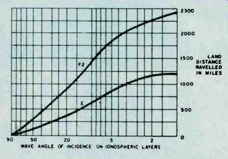
Fig. 3. The graph avoce shows the relationship between the angle of incidence of radio waves striking the "E" and "Fº" layers of the ionosphere and the distance which they will travel over land. Obviously, the lower the angle, the greater the distance travelled by the waves.
As signals travel a Great-C-ifele path, the high latitude paths will be the first to disappear as these reflection points are absorbed. As the storm continues, the lower latitude signal paths will disappear into the noise and, eventually, only signals from the south (in the northern hemisphere) will be heard. Those reflections points are outside the enlarged zone.
Sources of Information. How do you know if band conditions are good enough to warrant your time and effort to chase some DX? One time-consuming way is to tune across the bands, stopping at each signal encountered to see who it is.
An alternate method is to do some homework. A number of the amateur magazines offer long-range forecasts which are based upon extrapolations of current data. The newsletters offer more up-to-date forecasts, projecting just a week or two into the future.
Such newsletters include: the weekly hr report ( Greenville, NH 03048), the weekly West Coast DX Bulletin( 77 Coleman Drive, San Rafael, CA 94901), the bi-weekly Long Island DX Association Bulletin ( Box 173, Huntington, NY 11743), and the bi-weekly Mail-A-Prop ( 11307 Clara St., Silver Spring, MD 20902). Except for hr report, send a #10 SASE for subscription information.
A telephone call to Dial-A-Prop (516-883-6223) will deliver a message tape 24 hours a day, seven days a week.
Tapes are normally updated on Tuesdays.
Also, W1AW runs a weekly propagation bulletin amongst its daily airing of news and OSCAR bulletins.
Check a recent copy of QST for the schedule, or ask the ARRL ( Newington, CT 06111) for a W1AW schedule (send as SASE). The most timely information is provided by WWV. Unlike the other sources cited above, the National Bureau of Standard's propagation information is oriented for the engineer and scientist, and not for just the radio amateur.
WWV's Propagation Bulletin. At 18 minutes past each hour, WWV (on 2.5, 5, 10 and 15 MHz) broadcasts a tape supplied by the National Oceanic and Atmospheric Administration's Environmental Research Laboratories.
The message contains number counts of the solar flux, the A-index, and the K-index.
The solar flux is a measure of solar radiation: units range from 60 to 400. The higher the flux, the higher the MUF. In late 1978, the flux was averaging 160. The A-index is a measure of geomagnetic activity ranging from 0 (extremely quiet) to 400 (very disturbed)
units. An A-index of more than 20 usually wipes out polar path signals. Only on a very few occasions in the past five years have I seen this index exceed 100. The K-index is mathematically related to the A-index and is a measure of geomagnetic activity. Its range is 0-9.
As the flux and A-index counts are updated daily at 0000 GMT, and the K-index is updated every six hours at 0000, 0600, 1200, and 1800 GM1', it is possible to track short-run variations from day-to-day and from six-hour period to six-hour period.
In practical terms, you can build a set of references for yourself by noting the WWV counts under normal and abnormal conditions. The set of references may differ for different operators. The better the equipment and the antennas, the longer you have to work DX tinder worsening or marginal conditions.
Conclusion. I have only touched on some the principles and highlights of propagations and determining band conditions. One of the better books for those seeking further readings is a classic by Stanley Leinwoll, Shortwave Propagation, published by John F. Rider Publishers, New York, 1959. It would be worth hunting for on library shelves. For a detailed explanation of the H+18 WWV bulletin, pick up a copy of Introduction to Solar-terrestial Phenomena and the Space Environment Services Center Stephen J. Mangis, NOAAS Technical Report ERL 315-SEL 32, put out by the U.S. Government Printing Office, Washington, 1975.
Amateur band DX'ing doesn't have to be hit or miss.
Do a little reading and a little studying, and watch your DX totals go up.
========
=======
The UART
No, UART does not mean United Authority for Radio Tubes! It stands for Universal Asynchronous Receiver Transmitter. The UART is a special LSI integrated circuit that allows us to make a serial communications or I/O port for our microcomputers. With a single UART chip and a few other devices mounted on a blank S-100 prototyping card (such as the Vector products), we can make a serial I/O port rather easily. So who is the designer of a serial I/O for your microcomputer? Well, with the UART, thou art! Serial Data Transmission. Transmission of data from one unit to another might take place over a distance of a few feet, a few yards, several miles or across a continent.
Except in the shortest runs, e.g., from one equipment cabinet to another, it is usually more economical to use serial data transmission, in which the bits of the world are sent over the communications channel one by one. If we wanted to use parallel transmission, which is a lot faster, it would require not less than one wire or radio or telephone channel for each bit transmitted-and that can be expensive! In serial transmission, only one channel is needed, so that it is the lowest cost way of accomplishing the job! But microcomputers tend to have parallel organization.
The eight-bit data bus is a parallel structure. Before we can transmit the data over a serial channel, therefore, we have to assemble the data in serial form. This was once a bit . difficult, and required the interaction of both hardware and software, but today, we can make the job a lot easier because of the U ART. This LSI device will accept parallel format data on the transmitter inputs, send it out in serial form, and then reassemble it in parallel form on the receiver end. The typical UART contains both receiver and transmitter sections, so it may be used as either receiver, transmitter, or both.
The UART will also add certain bits needed in the parallel transmission. Figure 1 shows the general format for serial data transmission. The data line will sit HIGH (i.e. logical 1) when there is no transmission taking place.
The data word transmission begins with a start bit, which is a LOW condition. The transmission equipment, and the receiver section of the UART, sees the HIGH-to-LOW transition of the start bit as the signal that the data word is beginning. Following the start bit, are five, six, seven or eight bits of the data word. The typical UART chip is programmable to permit any of these data word bit lengths. The ninth bit could be a parity bit.
The concept of parity is used to check the data transmission for errors. The parity can be odd, or even, and this refers to the number of HIGH bits in the data word. the UART will set the parity hit HIGH or LOW to make the parity of the total word equal to that programmed into the system. Finally, there are 1, 1.5 or 2 stop bits. For most of our applications, we will use 2 stop bits, but some applications (like teletypewriters, for example) require 1.5 stop bits.
Fig. 1. The general format for serial data transmission. Fig. 2 shows a typical data word transmission without parity bit.
In this case, we are transmitting the word 101100101, and adding two stop bits. Fig. 3. shows the circuit design for a suitable clock, utilizing a 4060 chip.
Fig. 5. This is the block diagram of a typical UART. This particular device is the 1602, but it is pin-for-pin compatible with other devices such as the AY1013. The two sections, receiver and transmitter, are completely independent.
Figure 2 shows a typical data word transmission (without parity bit). In this case, we are transmitting the word 101100101, and adding two stop bits.
Clocking In. Data transmission means that the operations of the transmission are independent of a master system clock. But this does not mean that the clock must be accurate, and relatively stable. In general, RC-timed clocks are not acceptable, so we must use crystal control of the clock.
Figure 3 shows the circuit for a suitable clock, while Fig. 4 shows the pinouts for various division ratios of the internal counter of the 4060 chip used in the oscillator.
The 4060 chip is a multistage binary counter that includes its own oscillator stage.
The 4020 device, incidentally, is similar) except that it does not have the oscillator. Crystal Y1 will have a frequency selected by the desired baud rate of the data transmission, and the division ratio selected. The clock frequency applied to the input of the UART must he 16 times greater than the desired baud rate. If, for example, we want to drive a 300 baud printer from the UART, then clock frequency must be 16 x 300, or 4800 hz. If we select the 2" output of the 4060, the division ratio is 256, so the frequency of the oscillator should have a crystal frequency of 256 x 4800 Hz, or, 1228.8 kHz. A frequency of 1.229 mHz is a standard crystal frequency, so that could used. Trimmer capacitor C1 could then be used to trim the frequency to exactly 1.2288 mHz.
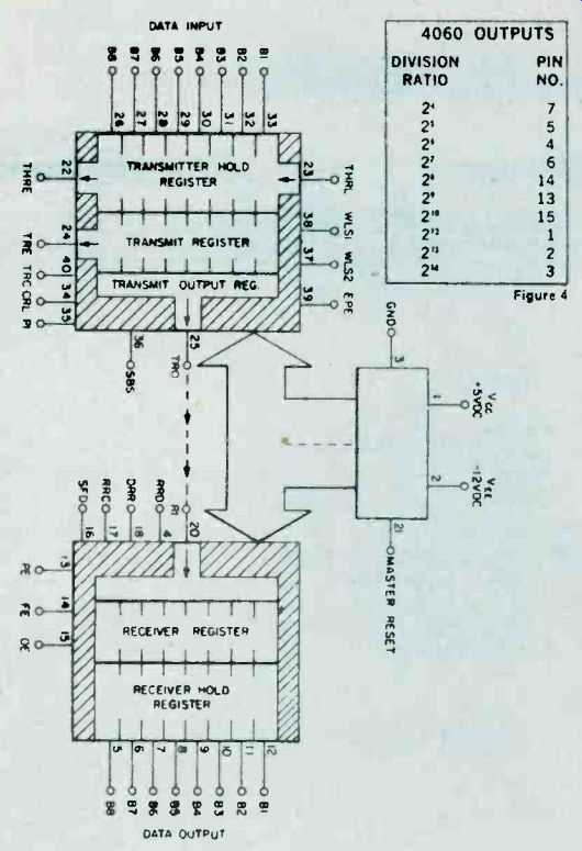
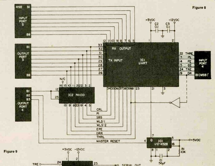
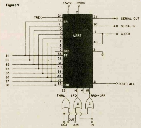
-------- The transmitter section circuit of the UART is shown in Figure 6. The receiver section of UART is shown in Figure 7.
The transmitter requires eight input bits, a clock at 16X the baud rate, and certain programming commands. The receiver section obeys the control signals wired into the transmitter section. Figure 8 shows the connection of the UART to a data bus. All the outputs of the UART are tri state. The methods shown in Figure 8 are basically for the 8080A device, but similar connections will allow use of the Z-80 and others. Figure 9 shows a method for connecting the UART to I/O ports of an existing microcomputer device,
The UART. Figure 5 shows the block diagram of a typical UART. This particular device is the 1602, but it is pin-for-pin compatible with devices such as the AY1013 and others. The two sections, receiver and transmitter, are completely independent except for the common connection tot he power supply and control section. We can use either the receiver, the transmitter, or both sections at once.
The transmitter section contains an eight-bit transmitter hold register, and a transmitter register. The hold register is a buffer, or storage area. When the THRL (transmitter hold register load) control line is brought LOW data on the eight input lines is loaded into register.
This data is transferred into the transmitter register for assembling into serial format and then for transmission.
The transmitter section also has certain other control lines, including the following: THRL, WLS1, WLS2, EPE, THRE, TRE, TRC, CRL and PI. These are defined as follows:
THRL WLS1,2 EPE THRE TRE TRC CRL PI
Transmit Hold Register Load Word Length Select Even Parity Enable Transmit Hold Register Empty Transmit Register Empty Transmit clock Control Register Load Parity Inhibit
The receiver section is a mirror image of the transmitter section. The serial data is disassembled from serial to parallel format, and the eight parallel bits are stored in a receiver register. The receiver output is the hold register which is connected to the eight-bit output lines. These output lines are tri-state types, so will float at a high impedance when not enabled. This feature allows us to connect the UART directly to a data bus, an application that will be covered later.
The receiver section also has its own signals: PE, FE, 0E, RRD, DRR, RRC and SFD; which are defined as follows: PE FE OE RRD DRR RRC SFD
Parity Error Framing Error Overrun Error Receiver Register Disconnect Data Receive Reset Receiver Clock Status Flag Disconnect
Basic UART Connections. One of the principal attractions of the UART device is the simplicity of its connection, allowing almost anybody to implement circuits based on the UART. The transmitter circuit is shown in Fig. 6, while the receiver circuit is shown in Fig. 7.
The transmitter requires eight input bits, a clock at 16x the baud rate, and certain programming commands. It also has a reset (pin no. 21 resets both the receiver and transmitter, as well as the status flags) control terminal.
The control flags must be set either HIGH or LOW, depending upon the requirements of the situation. We apply +5 volts to each line through a 1000 ohm, u-watt resistor, which sets the terminal permanently HIGH. A grounding switch will set the pin LOW if desired. In most of .our applications, I suspect that these pins will be HIGH. In that case, they are shorted together, and then connected to the +5 volt line through a single 1000 ohm resistor. In an application later in this article, we will allow setting of the control lines under program control.
The receiver section is shown in Fig. 7, and it is even simpler than the transmitter section if the transmitter section is also included in the circuit. The reason for this is that the receiver section obeys the control signals wired into the transmitter section. If the receiver section is to be used alone, however, we will also have to include the appropriate control signals. Otherwise the circuit is the same as in Fig. 7. We have a 16x clock, serial input, eight output data lines, and certain flags: DR, PE, FE, and 0E. We also have the DRR signal input. In the circuit shown the data received (DR) line is inverted and applied to the data receive reset (DRR) line. The inverter allows us to rest the DR flag.
UART Interfacing. The UART can be interfaced to the computer in several different ways. We can connect it directly to the data bus, either as a memory-mapped device or a dedicated I/O port, or, we can connect it directly to an I/O port of the computer. One of the applications to follow will allow you to interface the UART to existing parallel I/O ports of a microcomputer.
Figure 8 shows connection of the UART to a data bus.
This particular method of connection is possible because all of the outputs of the UART are tri-state. This means that, unless the output is enabled, the line floats at a high impedance to both ground and +5 volts. But, when the line is enabled, it will have a low impedance to +5 volts when HIGH and a low impedance to ground when LOW. In Fig. 8, we take advantage of this feature and connect the receiver output lines in parallel with the transmitter input lines and the data bus of the microprocessor. We can connect the master reset (pin number 21), to either the system power/on reset, or, to some point that can be used to reset the UART. The methods shown in Fig. 8 are basically for the 8080A device, but similar connections will allow use of the Z-80, 6502 or 6800 devices. Also, programming for each microprocessor will be different, so no examples will be given here.
A method for connecting the UART to I/O ports of an existing microcomputer is shown in Fig. 9.
The circuit in Fig. 9 uses two I/O ports to control the UART. Input port number 3 is connected to the receiver output lines of the UART. The receiver status flags are connected to input port number 4, although some of these will not be used by some programmers. There are two output ports used (3 and 4). Port number 3 is used to output the eight data bits, plus the control signals to the control inputs of the UART. Port number 4 is used to control the circuitry.
The 74100 device is used to store the control signals output from port number 3 so that the same port can also be used for the data bits to follow. But this IC is not strictly needed because the UART contains its own register to input the control signals. We could connect PI, SBS, WLS1, WLS2, EPE, and DRR to the output lines in parallel with the transmitter input lines. The CRL (control register load) line can then be brought HIGH
of it.
If you do want to buy a power mike, there are some things to remember.
First, not all power mikes fit all radios.
Second, it takes some skill to install a power mike. And third, if your radio has a mike gain knob on it, you already have a power mike.
Now, I don't want to offend you or make you feel unwelcome, but why don't you take your radio and get out?!
========
========
Inside Superhets
Born out of necessity during World War I, the superheterodyne receiver circuit toppled all existing conventional receiver types on electronics' popularity chart. And, to this day, none of the "conventional" radios of that era have been able to recapture electronics' limelight.
Stranger yet, every branch of electronics is still being swept along the path of Progress by a circuit that should have gone the way of the flivver and the flapper. From military and industrial to commercial and consumer-everybody who's ever seen a radio, and certainly a television set, has found himself staring face to face with a superheterodyne receiver.
The fact is, you'd he hard-pressed to find any up-to-date radio-even the integrated circuit-and-ceramic-transformer variety that doesn't somehow utilize the super het circuit.
After the First World War, the "All-American Five," at it was dubbed, took its place in living rooms and parlors from coast to coast. And it continues to be built today as its inventor generally conceived of it, way back when the circuit was made to track and help locate enemy aircraft spitting fire over French skies.
Narrow Squeeze. The super-hetero-dyne found itself ruling the, receiver roost largely because it had a redeeming quality no other receiver of that vintage era could boast. Called selectivity, this hitherto unheard-of quality endowed the superhet with the ability to select the particular station a listener wanted to hear (and later see), and reject all others. Indeed, it was a revolutionary step forward in receiver design.
But selectivity was hardly a quality needed back in grandfather's day. Why? First, grand-pop used to listen to signals sent by spark-gap transmitters. The primitive spark signals generated by those common-as-apple-pie transmitters were extraordinarily broad. It was like listening to the lightning crashes you can pick up as you tune across the dial of an AM radio during a thunderstorm.
More important, though, there were fewer signals on the air. So selectivity wasn't too important.
The year 1922 saw the meteoric rise of radio for entertainment and communication. As hundreds of stations took to the air it became apparent that the primitive receiving gear capable only of broad-bandwidth reception couldn't even begin to handle the impending traffic jam beginning to build on the airwaves. And the problems of receiving only one station, without an electronic cacophony drowning it out, takes us back even further into electronics' primeval time.
------p94 Fig. 1. Schematic representation of crystal radio shows how cat's whisker gently contacted diode surface in order to achieve demodulation of RF signal.
Earliest semiconductor diodes made were miniature crystal diode/cat's whisker affairs encased in glass package.
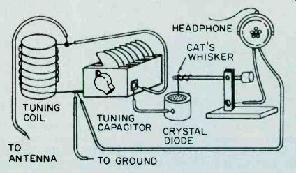
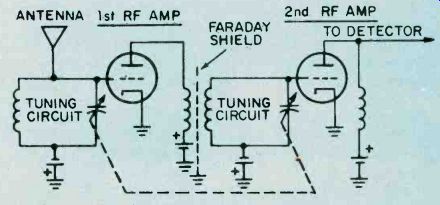
Fig. 2. Our schematic shows relatively advanced tuned radio frequency receiver. First TRFs had individually adjusted tuning capacitors; ganged units were still to be invented. By adjusting battery voltage twist ground, tuning circuit, radio gain's varied.
Cat's Whiskers and TRF. Digging through to the bottom of the twentieth century, we uncover two electronic fossils: the cat's whisker crystal receiver, and the tuned radio frequency (TRF) receiver. These were popular predecessors of the superhet circuit.
The crystal set had the least selectivity of either circuit, and what it did have was obtained mostly from one measly tuning circuit. Consisting of a coil and a homemade variable capacitor, these crude tuning devices could barely pick out a desired radio signal and, hopefully, reject all RF intruders trying to elbow their way into the listener's headphone on either side of the signal. The cat's whisker consisted of a strand of fine wire for gently probing, or tickling, the crystal's natural galena surface in order to locate its most sensitive point. Though the cat's whisker detector could extract audio signals from the amplitude-modulated radio frequency signal, the galena detector creasing the listener's chances of picking up stations other than the desired one.
Matters improved with the TRF receiver. It aimed for, and hit, sharper reception dead center, by adding more tuned circuits. This feat wasn't practical with crystal sets, because this circuit's inherent losses ran too high to gain any benefit from any additional coils.
The invention of the triode vacuum tube gave engineers the perfect amplifier device. Circuit losses could now be overcome with ease; the TRF took over where the cat's whisker left off, dooming the crystal set to mantelpiece and museum.
Three or four amplified radio-frequency stages were customarily added prior to the TRFs detector, all the while adding to selectivity's cause. However, all wasn't perfect in TRFville.
The amount of noise introduced by the tubes limited the number of TRF stages. So the Silver-Masked Tenor's strains could still be heard with those of the Clicquot Club Eskimos-but not by his choice, or that of the listener.
Pitching the Low Curve. The public soon learned that these newfangled TRF receivers weren't exactly the living end. The TRFs, as a rule, failed to perform satisfactorily as frequencies inched higher into kilohertz land. Seems that as the frequency of the signal went up, the TRF's tuned circuit efficiency for that frequency dropped almost proportionately.
To demonstrate this, look at our example. The bell-shaped curve represents response of a tuned circuit selecting some low-frequency station. The circuit delivers good selectivity, and interference on a slightly higher frequency is rejected.
But examine what happens when a similar tuned circuit is operated on a higher frequency. Although the curve's proportions remain the same, it's actually responding to a much greater span of frequencies. Now it's possible for two closely spaced stations to enter the response curve and ultimately be heard in the speaker.
Since tuned circuits grow more selective as frequency is lowered, wouldn't it be to our technical advantage to receive only low-frequency signals? This idea probably occurred to Major Edwin Armstrong, because his invention, the superheterodyne circuit, does just that.
Super-selectivity. By stepping signals down to a lower frequency than they were originally, the new circuit could deliver neat-as-a-pin selectivity on almost any band. The fact is, this development helped open the high-frequency bands, and by the 1930s virtually every receiver adopted the Major's superheterodyne idea.
The word "superheterodyne" is, by itself, revealing. It begins with super, for supersonic, referring to a new signal created within the radio. The generated signal is neither in the audio nor higher radio-frequency range, but in between. Hetero means combining, the dyne is force. The newly-created ten-dollar term, superheterodyne, neatly sums up this circuit's action.
Major Blocks. You can get a good picture of the superhet in its natural habitat if you look at our block diagram. Though our schematic shows. a tubed receiver, all equivalent stages tend to do the same job regardless of whether the receiver is transistor or tube.
Now that you know what the superhet does and how it looks, let's take a peek at how it works.
For sake of illustration, assume a signal of 1010 kHz in the standard BC band enters the antenna, and from there is sent down the line to the mixer.
But what, you ask, is mixed? Our frequency mish-mash consists of the different frequencies made up of the desired station on 1010 kHz, and' a second signal generated internally by the local oscillator. This oscillator perks at a frequency of 1465 kHz, for reasons which you'll understand in a moment.
True to its name, our mixer combines both signals from antenna and oscillator. And from these two frequencies, it delivers yet another frequency that is the difference between them namely 455 kilohertz. So far, our superhet circuit changed, or reduced the desired signal to a frequency having an intermediate value. Beating two frequencies together in order to produce a third signal is known by members of the Frequency Fraternity as mixing, heterodyning, or beating. And some engineers prefer to call the lowly mixer a converter; this term often appears in schematics. But whatever name you throw its way, the result is the intermediate frequency.
There's something else you should know about the intermediate, or IF, frequency. It always remains the same no matter what station you tune to. If you sweep the dial across the broadcast band in one continuous motion, the IF frequency remains constant. How's this accomplished? It's done by tuning the incoming signal simultaneously with the local oscillator. That's something akin to the mechanical rabbit which paces greyhounds at a race track. In the superhet a ganged tuning capacitor performs this dynamic duo feat.
Take a close look at the tuning capacitor, and you'll see physically smaller plates assigned to the local oscillator.
Since these plates are smaller than the antenna stage capacitor plates, the effect is to lower the capacity, and raise the frequency of the oscillator stage.
That's how the oscillator stage consistently produces a signal which is 455 kHz above the incoming frequency.
But why bother, you ask?
Fig. 3. Tuned-circuit bandwidth varies proportionally with frequency. Tuned circuit A, working at low frequency, rejects unwanted signal. Tuned circuit B, working at high frequency, can't completely reject undesired signal; interference results.
More Muscle, Too. When we convert each incoming station's frequency to the same IF, we gain another advantage besides better selectivity. A fixed-tuned amplifier always operates at higher efficiency than one which needs to muscle a multitude of frequencies.
There are fewer technical bugaboos in a one-frequency amplifier, so our tubes or transistors can operate more effectively' at this lower frequency. And, last but not least, circuit layout and wiring are less critical. All of this is well and good, but how do we actually extract our Top-Forty tunes, news, and weather from our super-duper-het? Sound Sniffing. The detector stage recovers original audio voltage from the station's signal. Since we're cranking the RF voltages through a superhet circuit, the RF signal did a quick disappearing act, only to appear as an IF frequency of 455 kHz. Though the original carrier (1010 kHz) is converted downward in frequency to 455 kHz, any audio voltage variations impressed upon the carrier remain the same. So if a musical note of 1000 Hz was sounded back in the radio studio, the note still remains that value in both RF and IF circuits, despite the mixing process.
Like a ladle skimming heavy cream off the top of a jug of fresh milk, the detector rectifies either the positive or negative-going portion of the carrier, skimming off the audio signals from the carrier. Though audio modulation appears during both positive and negative swings of an amplitude-modulated carrier, only one half of the available signal is used. If both positive and negative portions of the RF signal were detected simultaneously, the audio signals would cancel each other at the output! Now let's look at the stages of an ordinary solid-state superhet circuit that might be found in a common table radio or transistor portable.
Simplified Schematic. Our diagram is pretty typical of transistorized superheterodyne circuits. Of course, there may be variations on this circuit's theme, like the addition of an RF amplifier ahead of the mixer to improve sensitivity. The number of IF stages also varies with receiver quality, and specialized items such as filters may appear in ham and SWL rigs.
If you can follow our basic block diagram you'll have the key to virtually any solid-state superhet. In order to further simplify matters, many resistors and capacitors not essential to our tour through solid-state superhet country have been omitted.
Leading the pack on our superhet speedway is the antenna tuning circuit.
Loopstick antenna L1 grabs the RF signal out of the ether, and also serves in partnership with the tuning capacitor in the tuning circuit. You sharpies will also notice that the antenna tuning capacitor is mechanically joined to the oscillator tuning capacitor. (This is represented schematically by a dotted line.) Remember now, we want to develop the IF frequency. This ganged antenna/ oscillator capacitor ensures the necessary tracking of the local oscillator with the radio-frequency signal.
The oscillator frequency is developed by the oscillator portion of our variable capacitor, and coil L2. In our superhet's schematic, the oscillator signal is capacitively coupled from the oscillator transistor base and sent on its way to the mixer stage. The mixer, therefore, "sees" both oscillator and incoming station frequencies. The electrons from oscillator and antenna circuit get it all together in the mixer's base, producing our intermediate frequency.
Fig. 4. Virtually all superhets sold commercially are five-tub rigs; most are also, in terms of design, electrically and mechanically equivalent.
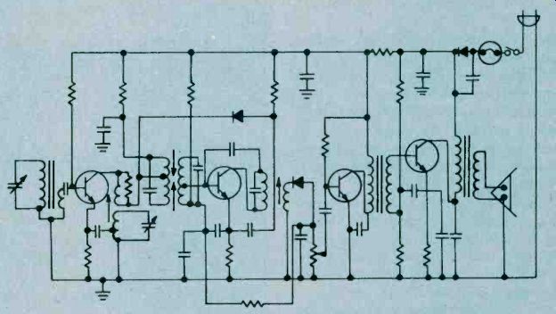
Fig. 5. Our schematic of a transistorized superheterodyne receiver is similar to the tubed superhet shown in Fig. 4. Biggest differences between the two are semiconductor diodes found in audio detector, AVC loop, and power rectifier stages.
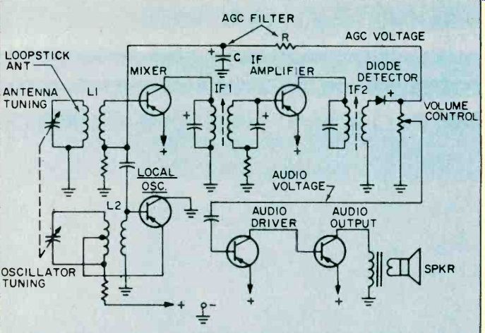
Fig. 6. Most superhets don't have separate local oscillator, mixer function; this schematic is more typical of BCB set. Communications-type receiver needs added usefulness of separate stages-it's easier to suppress images.
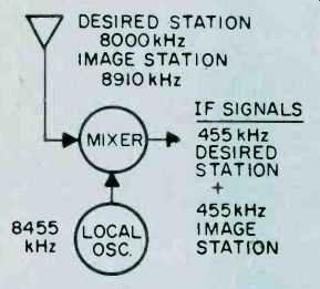
Fig. 7. Mixer is superhet's weakest link as signal handler. Too strong input signal can develop image frequency. Too much local oscillator signal pumped into mixer has same effect.
Fig. 8. Any superhet worthy of warming an amateur shack works around image problem with dual conversion. Combination of IFs puts image out of range of either stage.
If you could look at the mixer's output, you'd see more than just the IF signal. In fact, the mixer's load contains a jumble of frequency byproducts. As signals combine in this circuit, they add, subtract, and recombine in many ways.
It's as if you had to separate the wheat from the chaff with a pair of tweezers! Only the desired signal emerges from the mixer stage because intermediate frequency transformer IFI picks the proper signal to the exclusion of all the others. Now our freshly-created signal passes through a stage of IF amplification, and receiver selectivity is further whipped into shape by the second intermediate-frequency transformer, IF2.
As we've already described, the detection process takes place at the diode, regaining the radio station's original audio signal. This audio voltage is fed from the volume control to both audio stages where they're further amplified and sent to the loudspeaker.
The detector diode doesn't merely extract soul sounds from the ether; it also delivers a second voltage output. Called AGC (Automatic Gain Control), this voltage controls our mixer's amplification, preventing the speaker from blasting when you suddenly tune your radio to a strong station. In our simplified schematic, the AGC voltage is a positive-going voltage which increases proportionately with rising signal strength.
But before AGC can control receiver gain, it's filtered for pure DC in a resistor and capacitor network.
The result is a DC signal which can be used to control the gain of the mixer transistor. Thus, if a strong RF signal tries to muscle its way through this stage, the mixer is subjected to a higher bias voltage on its base terminal, which tends to put the brakes on our mixer's gain.
Pitfalls, Yet. Let's not lionize the king of receivers, though, for sometimes its growl turns to a puny purr. The biggest problem, and the most annoying, is a form of interference peculiar to the superhet known as an image. Produced by a mathematical mix-up, images are all of those undesired signals finding easy routes to travel through your receiver.
Take a look at our image explanation; you'll see the receiver is tuned to a desired signal of 8000 kHz.
The local oscillator generates a frequency of 8455 kHz, which places it exactly in our IF signal ball park. But note that a second station-a pop fly on 8910 kHz-also happens to be 455 kHz away from the local oscillator. For each oscillator frequency there are now two station frequencies giving identical IF frequencies. It's up to your receiver to strike out the image station. Otherwise, the RF ball game will turn into a rout! You might expect the receiver's antenna tuning circuit to completely reject the image signal. After all, it's supposed to be tuned to generate a very high IF frequency, positioning any images developed by the mixer well outside the tuning range of the antenna circuit. Looking at our example of a double superhet, you'll see one IF amplifier perking at 5000 kHz and another working on 455 kHz. Now if we receive an incoming signal on 8000 kHz, the local oscillator, now called a high-frequency oscillator, generates a frequency at 13,000 kHz, so the first IF signal works out to 5000 kHz. Your receiver would have to pick up a signal falling on 18,000 kHz to produce any image.
Naturally, the image frequency in this instance is significantly removed from the antenna circuit, so the image is greatly attenuated.
While high IF frequencies work well against image interference, they also revive Nagging Problem Number One: the higher the frequency of a tuned circuit, the poorer its selectivity. Since this situation also applies to IF stages, a second conversion is required, bringing the first IF signal down to 455 kHz, where we can sharpen our receiver's selectivity curve. That's how the double conversion receiver solves both image and selectivity hassles. Any ham or SWL rig worthy of an on/off switch is sure to have this feature. But don't think of dual conversion as a receiver cure-all.
Dual conversion is not usually found in entertainment receivers-radio broadcast and TV for example, because it's too sharp! High selectivity could easily slice away sidebands in an FM stereo program and kill its multiplexed channel, or rob a TV image of its fine picture detail.
But, for all its faults, tie basic super het circuit we've been talking about must be doing something right. Every year, several million superhets are sold in the U.S. Not bad for a circuit that might have gone the way of the hip flask, eh?
=======