Expand your universe with HE's pulsating phonoptic display. Ordinary LED chasers beware ....
LOOKING FOR a novel, economical, yet versatile LED display? Here is the answer to your dreams. Featuring an attractive matrix design, audio control input and a choice of three operating modes, the HE Starbursts adds a new dimension to conventional light-chasers.
Assembled on two printed circuit boards, the unit is designed around readily available CMOS chips and uses only a few other discrete components. The display is arranged as five semicircles of ten LEDs each which are illuminated in bands sequentially producing the illusion of either an expanding line of light or a band of light that grows outward and collapses. A novel bonus of the circuit design is the automatic mode where dots and bars are displayed alternately.
The audio signal pre-conditioner, clock oscillator and counter-decoder-driver circuitry is mounted on one board, whilst the other board holds the display and main decoupling capacitor. The circuit is powered by a single PP9 nine volt battery. Choice of a larger battery ensures longer life as currents of up to one hundred milliamps may be drawn when all the LEDs are lit. No provision is made for the battery or power switch on-board enabling the unit to be neatly boxed and mounted in any suitable remote position.
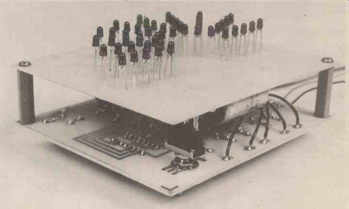
----- The two boards of the HE "Starburst," the switch
in the foreground controls the three modes of display.
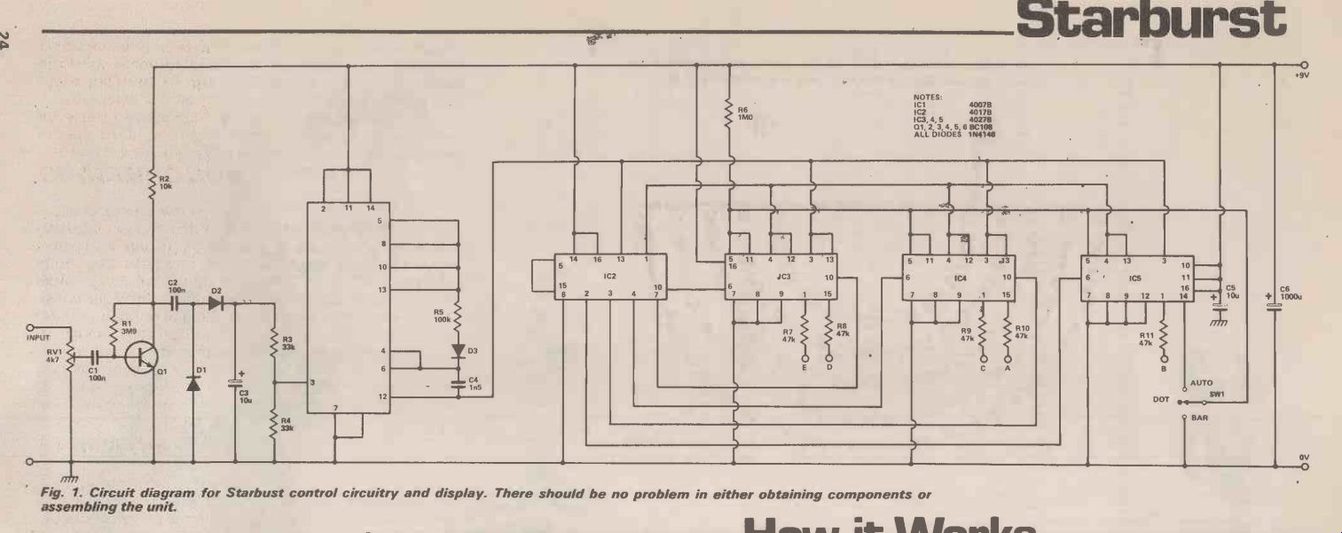
Fig. 1. Circuit diagram for Starburst control circuitry and display. There
should be no problem in either obtaining components or assembling the unit.
SEEING THE LIGHT
After applying power to the circuit, the LEDs will illuminate from the centre of the display outwards appearing as a bar or dots of light; or alternately depending on the position of mode switch SW1.
Application of an audio signal will cause the frequency of movement to increase. By adjustment of the input level and control RV1, the display can be made to follow the dynamic range of the audio input; in creasing in frequency as the audio input level increases in amplitude. Component values shown make the unit more sensitive to input frequencies above 1 kHz or so, and more responsive to melody lines in music and to vocal input.
-----------------------
How it Works
IC1 is an oscillator whose frequency can be con trolled over a limited range by a voltage applied to pin 3. As the voltage rises, the frequency increases.
The block diagram does not give much away so the important parts of the circuit have been drawn in simplified form in figure 2.
As can be seen, the chip contains two pairs of complementary transistors which are here con nected as inverters and one single transistor (pins 3, 4, 5) which operates as a voltage controlled resistor. It also contains another complementary transistor which is not used here.
Operation of this network is more easily under stood by representing it as shown in figure 3. It is the same circuit, though the complementary transistor inverters are now shown in block diagram form. The remaining transistor and the resistor and diode together form the timing resistance Rx and can be considered as a single resistor.
If the circuit is redrawn.(fig. 4), it will be familiar as a conventional CMOS oscillator. The resistor and diode are simply there to modify the duty cycle of the oscillator in order to produce a greater control range from the circuit.
The control voltage for IC1 is derived from the audio signal input to Q1 via RV1 , C1. The amplified signal appearing at the collector of Q1 is coupled via C2 to rectifiers D1, D2 which charge C3. R3 and R4 tap off a proportion of the voltage across C3 as well as providing a discharge path for this capacitor. Comparatively high values can be used for these resistors as there is negligible loading by the very high input impedance mosfet in IC1.
The pulses from oscillator IC1 (pin 12) clock five of the flip-flops in IC3, 4, 5 and the decade counter-decoder IC2 which produces a logic 1 high level at its outputs in turn. These signals could be fed to the transistor LED drivers directly but instead are processed by five of the J K flip'-flops in IC3, 4, 5. It is this that enables the different modes of operation from the display. The sixth flip-flop is clocked each time a display sequence is completed and its output consists of alternate logic 0s and 1s.
Briefly, these 4027 chips each contain two flip flops whose outputs following a clock pulse depend on the state of two inputs: J and K. In this design, one input (J) of the five flip-flops is driven by the outputs from the 4017 whilst the other input (K) controls the form the display will take. All the K inputs from these five flip-flops are commoned and brought out to SW1 where a logic '0' or an alternating logic signal is available from the sixth flip-flop. When SW1 is in the' center-off position, the K inputs are pulled up to a logic '1' by R6 giving a dot display.
The outputs from J K flip-flops control transistors Q2-Q6 which drive the LED display. C5 and C6 are power supply decoupling capacitors.
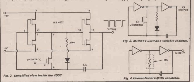
Fig. 2. Simplified view inside the 4007. Fig. 3. Fig. 4. Conventional CMOS
oscillator.
-------------------------
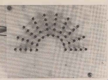

--- The display board viewed from above, the effects, especially
when in the "audio" mode are quite exciting, to say the least.
--- PCB foil pattern for the "Starburst" display board, no problems here, as always take care with your soldering.
LUCKY NUMBER
At first glance, it would appear that the way to produce a display such as the one described above might be to use a "bargraph" chip driven from a ramp whose frequency would be controlled by the audio signal. However, the CMOS family contains some not so popular but nonetheless versatile chips which enable an economical yet sophisticated circuit to be produced. By coincidence, all the chips in this project contain the number seven in their device code. They are the 4007, 4017 and 4027.
SEVEN UP
The mainstay of the circuit is the ubiquitous 4017 decade counter-decoder whose outputs are processed by the 4027 chips to produce the logic control signals for the display driver transistors.
The 4007 is probably the least familiar device. It is not strictly speaking a logic chip as it contains only three pairs of complementary metal oxide silicon transistors which may be interconnected in a number of different ways. They ,are configured here as a novel voltage-controlled oscillator which provides the clock drive signals for the 4017 counter and 4027 JK flip-flops.
Operation of this part of the circuit is described in more detail in 'how it works'.
CONPSTRUCTION
The unit is assembled on two PCBs. Use of our PCBs will greatly simplify construction as well as enabling an attractive free-standing display to be produced.
Wire links should be inserted first and soldered into place followed by the IC sockets. Use of sockets is strongly recommended. Next, insert the resistors, capacitors and-transistors and diodes. Do not insert the CMOS chips at this stage. Note that some of the links pass under the IC sockets. If you do forget to put one in and discover later that it is inaccessible simply use a piece of insulated wire on the underside of the board to complete the connection.
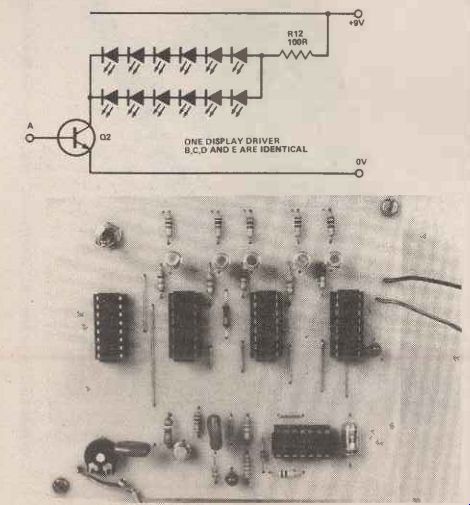
The LEDs are wired in series-parallel and failure of one will cause the other four in an arm to extinguish. The display board can be tested as it is assembled by use of a separate nine volt supply. Insert and solder into place C6 ensuring correct orientation then connect the positive lead of the battery as shown on the overlay and make up a length of wire in series with a 330-ohm resistor.
Connect the free end of the resistor to the negative terminal of the battery. Then as assembly of each arm of LEDs is completed, touch the free end of the wire from the resistor to the connector pads on the PCB (shown going to resistors R12 to R16 on the overlay). The LEDs should light. Failure to do so indicates an open circuit or reversed LED. Check for this condition by shorting each LED in turn until the display lights and replace any faulty ones ensuring correct orientation. A short lead, indent or flat on the plastic encapsulation usually indicates the cathode. We used red LEDs. In fact green or yellow LEDs will not work with a nine volt supply as they have a higher forward voltage drop.
Once satisfied that the display board is working correctly, make the remaining interconnections between the boards. We mounted SW1 on the main circuit board, there's plenty of room. Insert the ICs observing the usual CMOS handling precautions and connect a nine volt battery. The display should illuminate. If all is well, connect an audio signal to the input and adjust RV1 for satisfactory operation. Check that operation of SW1 causes the display mode to change.
We used the earphone socket of a transistor radio as an audio source though any signal of around 1 volt peak to peak will do. Finally, disconnect the battery and assemble the boards together using spacing pillars to separate them. That completes construction so switch on, plug in and flash out!
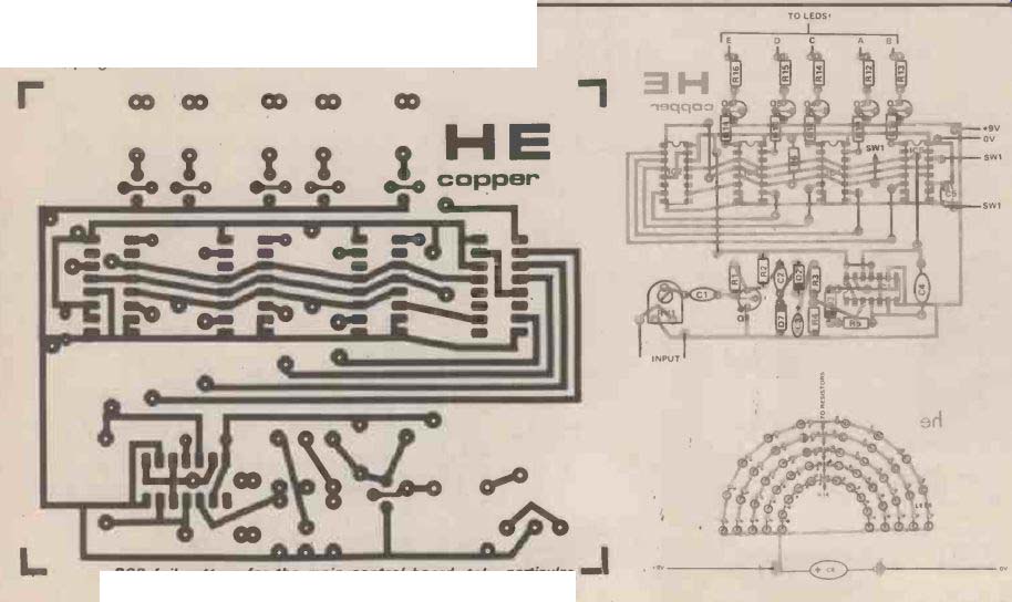
------ PCB foil pattern for the main control board, take particular
care when soldering in the ICs to avoid any solder bridges.
---------------------
Parts List
RESISTORS
R1 R2 R3, 4 R5 R6 R7,8,9,10,11 R12,13,14,15,16
CAPACITORS
C1, 2 C3, 5 C4 C6
SEMICONDUCTORS
IC1 IC2 IC3,4,5 Q1,2,3,4,5,6 D1,2,3 LEDs (all 1/4W, 5%) 3M9 10k 33k 100k 1M 47k 100R 100n polyester 10µ tantalum 1 n5 polystyrene 1,000 µ electrolytic 4007B 40178 40276 BC108 1N4148
0.1 25" red (50 are needed if our display board is used)
MISCELLANEOUS
SWI SPDT center off switch. PCB PP9 battery, connectors. Approximate cost (mult by 1.4 for dollar) £10.00.
Buylines
All the components for this project should be readily available from the usual suppliers. It is worth 'shop ping around' for the LEDs as these are sometimes offered in quantity at a discount.
(adapted from: Hobby Electronics magazine, Sept. 1979)
Also see: