In this Section AM/FM stereo tuner and amplifier circuits operation and troubleshooting will be explained.
FM STEREO RECEIVER CIRCUIT (GE TU-100)
The General Electric TU100 FM stereo receiver circuit is shown in the semi-block diagram Fig. 1. The detected FM or FM stereo signal is fed to the base of transistor Q14, the composite signal amplifier. FM audio or composite FM stereo signals are amplified and appear in the collector circuit of Q14. The FM audio or composite FM stereo signals then pass through the band pass and 67 kHz filter to the stereo detector and de-emphasis circuits. Control R98 and capacitor C116 located in the emitter circuit of Q14 form the stereo balance control. Adjusting R98 establishes feedback to increase or decrease the gain in the L-R signal area.
Transformer T8B in the collector circuit of Q14 selects the 19 kHz pilot signal when it is present. The 19 kHz pilot signal is amplified by Q13.
Control R96 and R95 form a series voltage divider network to supply base voltage to Q13. Thus, R96 acts as a threshold control by establishing the gain of Q13. The factory adjustment of R96 is to set the gain of Q13 for threshold at 6 percent of the pilot signal level. That is, Q13 will conduct and turn on Q11, thus lighting the FM stereo lamp indicator.
Transistor 19 in the collector circuit of Q13 is tuned to 38 kHz, the second harmonic of the 19 kHz pilot signal. The 38 kHz signal is amplified by the doubler stage Q12. T1OB in the collector circuit of Q12 is inductively coupled to T10A, thus adding the regenerated 38 Hz sub-carrier signal to the stereo detector circuit to detect the left and right FM stereo signal.
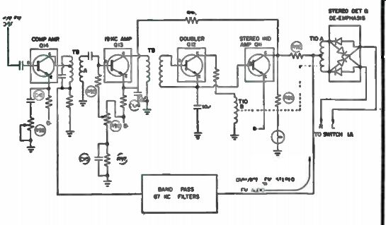
Fig. 1. Block diagram for stereo receiver.
When the 38 kHz regenerated signal is present at T9, capacitor C101 becomes charged and causes the DC level at the base of Q11 to go more positive, thus causing Q11 to conduct. Since the stereo indicator lamp is in series with the collector of Q11, it will light when Q11 is driven into conduction by the 38 kHz signal.
A portion of the collector voltage of Q11 is fed back to the emitter of Q13 via R91 to increase the forward bias and gain of Q13, firmly locking the circuit in tight. This prevents the FM stereo circuits from switching back and forth from stereo to monaural on weak or fading station signals.
AM/FM IF AMPLIFIER CIRCUIT (G. E. TU-100 CHASSIS)
Transistors Q2 and Q3 serve as IF amplifier stages for both AM and FM. The IF coils are unusual in that they are capacity coupled as opposed to inductively coupled. The circuit for this IF stage formed by T3 and 14 is shown in Fig. 2. Note that 13 consists of the IF coil for FM and AM in the collector circuit of Q2, while 14 consists of the tuned coil for FM and AM in the input circuit of Q3. The top winding of each IF coil is the FM section.
13 and T4 are located so that inductive coupling between coils is not possible. Note that the FM and AM coil windings of 13 are wound on one coil form, while the FM and AM coil windings of 14 are wound on another form. Both 13 and 14 are enclosed in a shield. The FM and AM IF coils are slug tuned. Capacitor C18 couples the FM IF signal from 13 to 14. C19 couples the AM IF signal from 13 to 14.
With an FM IF signal (10.7 MHz) present at 13, the following conditions exist. The bottom winding of 13, (AM section) acts as a choke or open circuit to the FM IF frequency. This places C17, 820 pf and C16, 140 pf in series across the top winding (FM section) of 13.
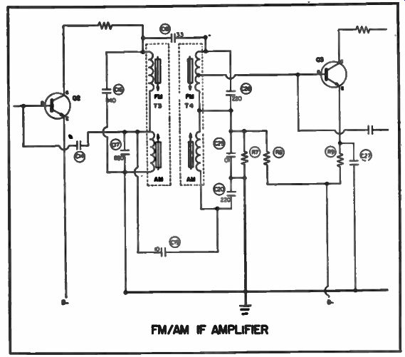
Fig. 2. FM/AM IF amplifier circuit.
The two capacitors in series then act as the resonating capacitance for the top half of 13. C16 and C17 also act as a capacitive voltage divider from which C14 receives a neutralizing voltage to feed back to the base of Q2.
C18 acts as a coupling capacitor to couple the FM IF signal to the top winding of T4. The bottom winding (AM section) of 14 acts as a choke or open circuit to the FM IF signal. Capacitor C26 acts as the resonator capacitor across the top winding (FM section) of 14. A capacitive voltage divider is formed by C25 and C26 so that the correct amount of AC signal is fed to the base of Q3 through the tap on the FM coil of T4.
When we consider an AM IF (455 kHz) signal at the top of 13, the following conditions exist. The top winding (FM section) of 13 acts as short circuit to the AM IF signal, thus C16 and C17 are in parallel across the AM winding (bottom half) of 13. Capacitive voltage division takes place in C16 and C17 to supply the neutralizing voltage source for C14 to feed back to the base of Q2. C19 acts as a coupling capacitor to feed the IF signal to the AM (bottom winding) section of 14. Capacitors C20 and C25 are then in series across the AM (bottom winding) section of 14. Since the point between C20 and C25 is grounded, a capacitive voltage divider is formed so that the correct amount of AM signal is fed to the base of Q3 through the FM (top winding) section of 14. The FM (top winding) section of 14 acts as a short circuit to the AM IF signal when coupling the AM IF signal to the base of Q3. Capacitors in parallel with the IF coil windings and coupling capacitors are mounted externally from the IF coils as opposed to being an integral part of the IF transformer base.
AM/FM TUNER POWER SUPPLY CIRCUIT
The voltage regulator circuit in Fig. 3 requires an input voltage of -22 to -35 volts DC to supply the AM/FM tuner with - 12 volts DC ± 5% of operating power. Voltage regulation is accomplished by Zener diode D5, Q9, Q10 and associated components in a direct coupled circuit configuration. Transistor Q9 is forward biased by resistors R60 and R65 and Zener diode D5. Transistor Q9 (PNP) is used as a voltage amplifier and polarity inverter to forward bias Q10 (NPN) into conduction and complete the voltage regulator circuit. Current limiting is performed by resistors R60, R65, R66, R67 and D5. Additional power supply filtering is accomplished by C86. Capacitors C87 and C88 filter any unwanted transient AC voltages that may be present in the input DC voltage and cause Q9 and Q10 to oscillate. Use a scope on base of Q9 to check for any oscillation that may be caused by an open filter capacitor(s). NOISE AMPLIFIER (SYLVANIA) This noise amplifier and auto mono/stereo switching circuit is used in some Sylvania stereo tuner systems. In the FM multiplex signal, noise becomes more of an annoyance than in the FM mono signal, due to the AM characteristics of the multiplex signal. These AM characteristics permit noise to ride into the system, producing objectional listening.
The noise amplifier transistor Q22, (see Fig. 4), is coupled to the FM detector chip, IC2, through a 330 pF capacitor, C124. When the noise level increases in the FM multiplex signal, the Q22 transistor amplifies the noise, and feeds it through C152 to diode SC4. The noise signal is rectified by SC4, producing a negative DC output. This voltage reduces the forward voltage applied to pin 4, IC4, by the resistance network, R126, R124, and SC4, causing Q31 to turn down. Its collector voltage rises, turning on the Darlington amplifier, Q29-Q30. The emitter voltage rise at Q29 turns on Q28, as its collector is connected to the junction of R14 and R16. It brings this junction point to ground.
The composite signal fed from Q4 to Q11 is shorted, killing the 19 and 38 kHz circuits. However, the composite fed from Q4 to Q8 drives the differential amplifier and synchronous detector through Q22. Without the 38 kHz switching signal, the decoder becomes an amplifier feeding the audio signal onto the stereo power amplifiers.
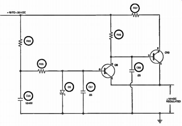
Fig. 3. Voltage regulator for stereo receiver.
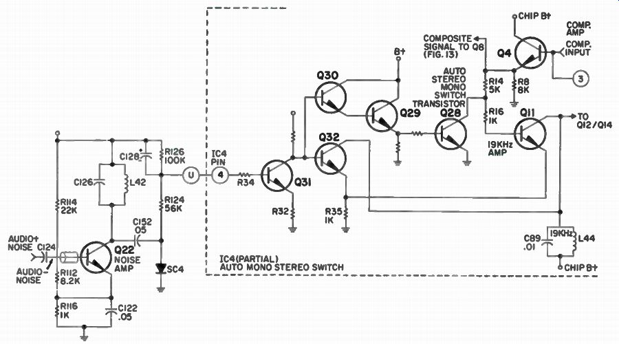
Fig. 4. Mono/Stereo 1C4 auto switching circuit.
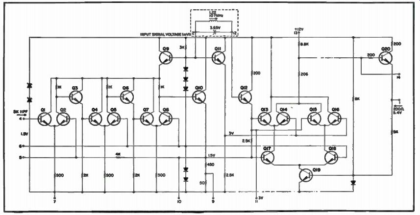
Fig. 5. Circuit inside FM detector IC.
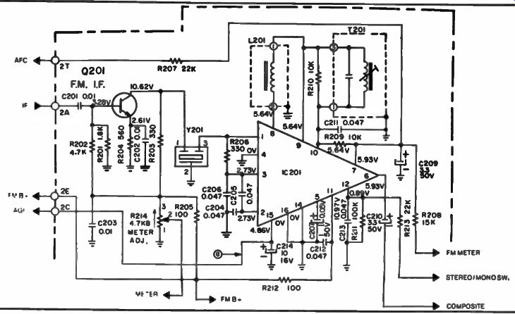
Fig. 6. FM IF chip circuit.
FM DETECTOR (IC2) SYLVANIA STEREO
This FM detector, IC2, shown in Fig. 5 has internal voltage regulation and good sensitivity. The FM detector chip has 20 transistors, 21 resistors, 6 diodes and two Zener diodes. This chip is an FM limiter, quadrature oscillator, and a product detector. FM limiting is done by three stages of differential amplifiers, using 9 transistors.
The quadrature oscillator Q12, and its external tuned circuit L22, receives the 10.7 MHz signal via a capacitive coupling in the L22 assembly.
Coil L22, adjusts both the phase and frequency of the 10.7 MHz quadrature oscillator signal and applies the correct phase to the bases of Q13, Q14, Q15, and Q16 in the product detectors. The FM IF signal is applied to the emitters. The audio or composite multiplex signal is recovered by comparing the phase and frequency of the two 10.7 MHz signals across the emitter base junction of the product detector transistors.
IF CIRCUIT STRIP--FM STEREO (ZENITH)
This W strip circuit consists of IF transistor Q201, ceramic filter Y201 and IC201, which includes gain, limiter, and quadrature stages. Note FM IC circuit in Fig. 6.
As a reminder, ceramic filters are highly selective devices. Being made as fixed frequency devices, they may fall into one or more overlapping groups of frequencies. The center frequency of a ceramic filter may not be at the designated IF frequency (such as 10.7 MHz). The filters may be grouped as shown in Fig. 7.
When aligning a ceramic filter, set the signal generator to the frequency of the ceramic filter, then align the IF. The FM-IF, IC201 is preceded by Q201 (first FM IF) and ceramic filter Y201, with input to IC201 being at pin 1. This IC's internal circuitry (note block diagram in Fig. 8) consists of three IF amplifier stages with level detectors for each stage, a doubly-balanced quadrature detector, an AFC amplifier, an audio amplifier and an internal voltage regulator.
Outputs of IC201 include delayed AGC (pin 15), AFC and FM meter (pin 7), composite audio (pin 6) and mute control which is located at pin 12.
Delayed FM AGC voltage is developed internally within IC201.
Output of the first IF amplifier is amplified by its level detector. Since the first IF amplifier is the last IF amplifier to go into limiting, the level detector will develop a current which will appear as a voltage across C214, at IC201 pin 15. This is the delayed AGC voltage which is applied to the base of Q1 (FM-RF). When the IF signal level is sufficient, Qrs base voltage is lowered, lowering the gain of transistor Q1.
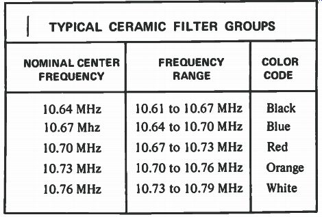
Fig. 7. Ceramic filter table.
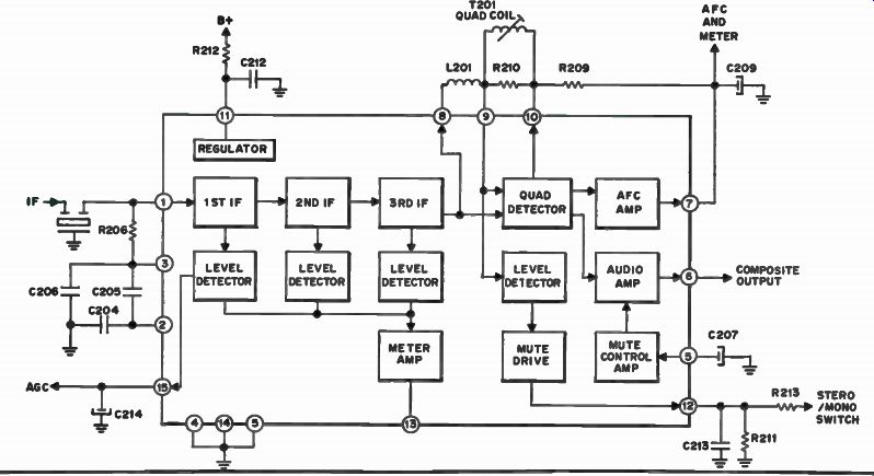
Fig. 8. Block diagram of FM IF chip.
FM-QUADRATURE DETECTOR
The amplified and limited IF signal appears at IC201 pin 8 and is coupled via L201 to pin 9, the Quadrature detector. Connected externally, between pins 9 and 10 is Quad coil 1201. Voltage appearing across 1201 is a function of the signal frequencies appearing at the ends of T201. Signals at these pins will be 90 degrees apart, or in quadrature, resulting in the circuits being called a quad detector. Signals at the center frequency will produce equal voltages at pins 9 and 10, while frequencies off of center frequency will create different voltages on pins 9 and 10. Since this IC uses a differential circuit, only the difference of the signals appearing at pins 9 and 10 will be amplified. If pins 9 and 10 have identical signals, the signal will not be amplified.
Tuning Meter Operation
The tuning meter is common to both AM (maximum reading) and FM (zero center reading). Diode CR253 is the AM meter rectifier, while FM meter voltages comes from pin 7 of IC201 (FM-IF). Bandswitch S1, selects the appropriate meter voltage. Meter adjustment resistor R214 is adjusted to set zero center for the meter as part of the FM alignment procedure.
Stereo/Mono Switching
Pin 12 of IC201 provides a control voltage which is used to control the stereo/mono switching of the stereo multiplex decoder, IC301.
FM MULTIPLEX CIRCUIT OPERATION (ZENITH)
A block diagram of IC301 is shown in Fig. 9 of the FM Multiplex Decoder. The circuit for the IC301 decoder is shown in Fig. 10. This decoder uses a voltage controlled oscillator (VCO) as part of a phase locked loop (PLL). IC301 has three basic functions.
• Regeneration of the 38 kHz subcarrier frequency.
• Stereo indicator switching.
• Decoding (Matrixing L+R and L- R/38 kHz to provide L and R outputs).
The composite signal (L+R, L- R, 38 kHz) from pin 6 of the FM-IF (IC201) is connected to the input (pin 2) of IC301. This signal is amplified and then coupled from pin 3, via C301, to pin 13. It is also internally connected from the amplifier to the demodulator. From pin 13 the composite signal is divided into two paths (one is the phase detector and the other is an amplitude detector). Near the middle of the top row of blocks (at pin 16) is the voltage controlled oscillator (VCO) which runs at 76 kHz. Its free running frequency is determined by C305, R305 and R316.
The VCO output goes to two divide-by-two stages, resulting in outputs of 39 kHz and 19 kHz. The 19 kHz is available at pin 12 for frequency measurement.
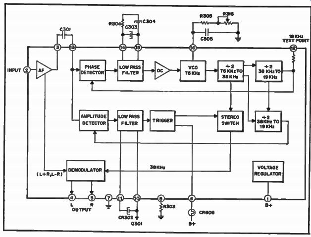
Fig. 9. Multiplex IC block diagram.
Proper adjustment of the VCO frequency is made by connecting a frequency counter to pin 12 of IC301 and adjusting R316 until the frequency counter reads 19 kHz. If you do not have a frequency counter, use the following technique. A station broadcasting a stereo program is tuned in, R316 is then adjusted until the stereo indicator turns on, followed by adjustment of R316 to the middle of the turn-on range.
The 19 kHz signal at pin 12 is fed back to the phase detector, where the phase and frequency of the 19 kHz signal is compared with the 19 kHz in the signal applied to pin 13. Any difference is fed to the low pass filter (including external components) at pins 14 and 15. Output of the low pass filter is converted to a DC correction voltage that is applied to the VCO to correct for any changes in the VCO frequency.
Also at pin 13 is the amplitude detector which receives both the input 19 kHz signal and the 19 kHz signal from a third divide-by-two stage.
Incoming levels of the 19 kHz pilot level will be sensed by the amplitude detector. If the pilot level exceeds a minimum level, the amplitude detector will output a signal to the low pass filter (including external components) at pins 10 and 11 and also to the trigger stage. When the trigger stage is turned on it will activate the stereo indicator, CR606, via pin 6 and also will enable the internal stereo switch circuitry to pass 38 kHz to the demodulator. In the demodulator, the sum (L+R) and difference (L- R) and 38 kHz signals are combined to derive both the "L" channel and the "R" channel.
Automatic stereo/mono switching is determined by the IF signal level. This signal is converted to a control voltage which is available at pin 12 of the FM-IF, IC201. Voltage on pin 12 will be high at zero IF level but, as signal level increases, voltage at pin 12 drops as shown in Fig. 11.
This voltage will be coupled, via R213, to Q301 (multiplex noise filter)
where it will be amplified. When the IF signal is low, a high voltage appears at IC201 pin 12, it is amplified by Q301 and is then applied, via R306, to pin 10 of the multiplex decoder, IC301. IC301 pin 10 is the output of the amplitude detector filter connected between pins 11 and 10. When a high control voltage is applied to pin 10, it will effectively switch off IC301's internal switching circuit, causing the circuit to revert to mono operation.
As the IF signal level increases, voltage at IC201 pin 12 will drop, Q301 will cut-off, voltage on IC301 pin 10 will go low and the incoming 19 kHz pilot signal will control the internal switching, passing stereo to IC301 output pins 4 and 5 of the chip.
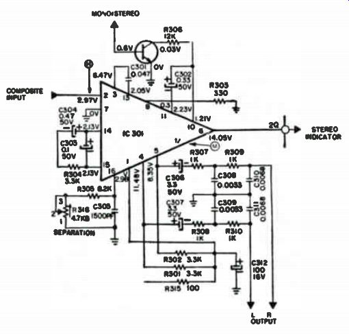
Fig. 10. FM Multiplex circuit (chip).
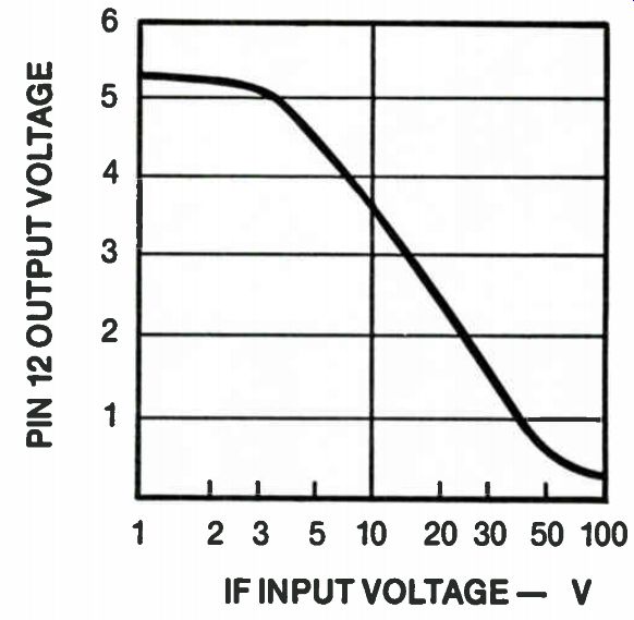
Fig. 11. Voltage chart.
-----------------
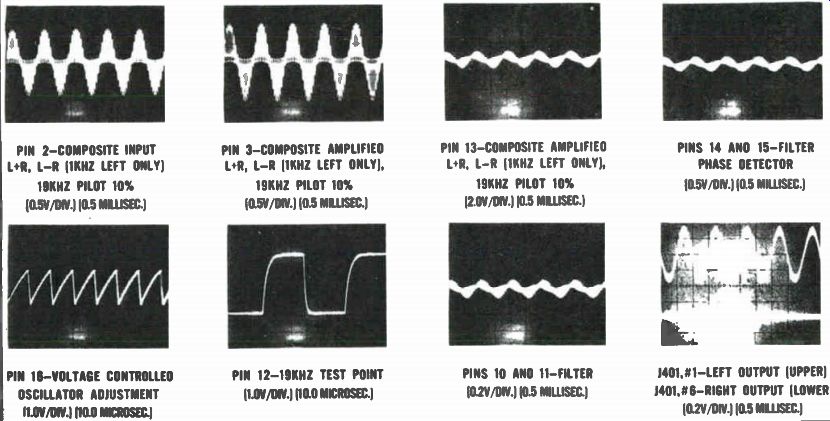
Fig. 12. Multiplex decoder scope waveforms.
------------------
A regulator is located within IC301 (connected at pin 1) and supplies most stages, while unregulated voltages power the other stages.
Stereo Indicator Lamp (CR606) is connected to IC301 pin 6. When IC301 detects the presence of a stereo pilot signal, pin 6 will be enabled (go high) and a path will be completed through CR606 to a B+ voltage point on the power amplifier chassis.
Typical waveforms found in this FM Stereo Multiplex Decoder are shown for all active pin-outs in Fig. 12.
Multiplex Alignment Comments
Before any attempt is made to align, or service, FM multiplex circuitry, you must be sure that the RF, IF, and detector alignment is correct, and that the receiver functions OK on monaural station signals.
Multiplex generators are good troubleshooting devices because they provide a composite multiplex signal as well as an RF signal (which is FM modulated by the composite multiplex signal). The composite signal is very useful since it can be used in signal tracing the multiplex portion of the receiver. It's not recommended that multiplex alignment be made using the composite signal injected at the output terminal of the detector since there is always some phase shift occurring in the RF, IF or detector circuits. As a result, multiplex alignment made by a signal injected at the detector input would not be correct. For proper multiplex alignment, the composite signal must FM modulate the RF carrier and then be fed into the FM antenna input. With the signal injected in this manner, the multiplex alignment would be the best that could possibly be obtained.
RF signals should be injected at a point in the FM band where no signal is present. If at all possible, this should be at a frequency near the middle of the FM band. Tune the FM receiver to this point and adjust the RF frequency adjustment on the generator to this same frequency. The AGC voltage developed in the receiver should be maximum. An AGC voltage a lot less than this could indicate that the RF frequency is tuned to an image.
Stereo Tuner Troubleshooting Tips
Should a problem arise in aligning the FM multiplex portion of the receiver, you must determine whether the fault lies in the RF, IF, and detector portions of the receiver, or whether the trouble is in the multiplex portion. The composite output of the multiplex generator can be injected at the output of the detector to help determine the area of difficulty. To reproduce possible extraneous signals coming through the detector, short the detector primary with a jumper lead. The waveforms and their amplitudes may vary slightly from chassis to chassis, however, they are quite indicative of what will be seen when signal tracing the multiplex circuitry.
If all of the waveforms are similar in form, it can be assumed that the multiplex portion of the receiver is functioning properly and the problem area is ahead of this in the FM receiver. If any of the scope waveforms are missing at a later point but are apparent at a previous point, circuitry between the two test points should be checked.
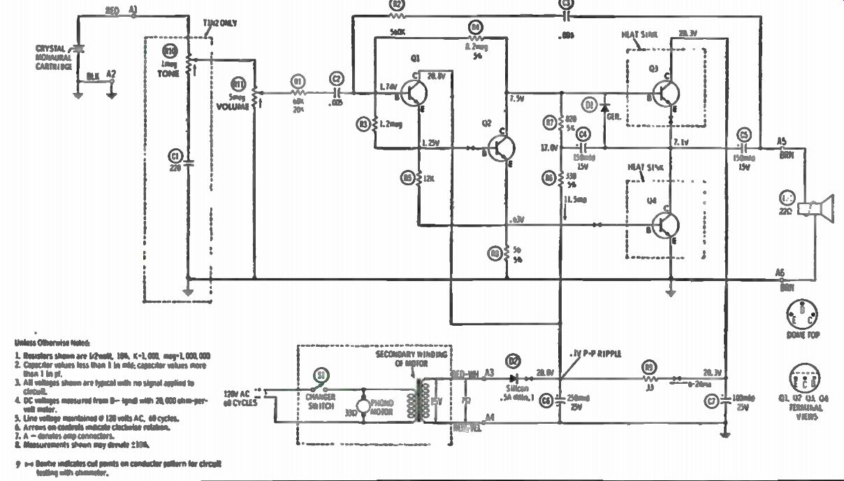
Fig. 13. Mono audio amplifier circuit (transistor).
AUDIO AMPUFIER CIRCUITRY (MONO-STEREO)
In the circuit shown in Fig. 13 the signal from the crystal cartridge is fed to the base of input transistor QI via the tone control. The signal goes onto the volume control, the isolating resistor RI and coupling capacitor C2.
QI is a high Beta NPN silicon device operated class "A" and connected in the common collector mode. The stage has the following characteristics - high input impedance - low output impedance - output signal has same phase as input - high current gain.
There is 7 db of feedback from the output fed to the base of Q1 via R2 and C3 to compensate for circuit nonlinearities. The output signal at the emitter of Q1 is directly coupled to the base of Q2. Transistor Q2 is a class "A" operated NPN silicon unit functioning as a phase splitter-driver. Q2 supplies driving signals for both output transistors. At its emitter, a current amplified signal in phase with that at its base is available for driving transistor Q4. At the collector of Q2, a phase inverted voltage and current amplified signal is used for driving Q3.
Q3 and Q4 are both NPN silicon units capable of 700 mw of power when heat-sinked. Both are forward biased by a positive base voltage.
Since the signal fed to the base of Q3 is of the opposite phase from that at the base of Q4, forward bias is increased on one transistor by one half of the signal, while the other half increases the forward bias of the other. Thus, when class "B" operation is attained, each amplifies only one half of the signal. Q3 is connected as a common collector, thus, its output has the same phase as its base. Q3 provides power amplification of the positive half of the signal across the speaker load. Q4 is connected as a common emitter, and therefore, supplies a power amplified, phase inverted signal to the speaker load. In this way, Q4 provides an amplified negative going signal at its output load.
Two circuit components which play a very important part in this circuit's operation are capacitor C4 and diode Dl. Their functions are as follows. C4 in series with C5 and the low impedance voice coil of the speaker act as a B+ filter and greatly reduce hum and ripple. C4 also provides a boot-strapping effect by supplying driving power to the collector of Q2, thus making possible wider signal swings before limiting takes place.
Diode D1, increases greatly the ability of this circuit to produce rated output power. DI operates in the following manner. When Q2 conducts heavily with the application of a high amplitude signal at its base, its collector voltage drops rapidly due to current flow through the high series resistance of R7 and R6. When this potential drops slightly below the charge on C5, D1 becomes forward biased and allows the charge stored on capacitor C5 to furnish much needed driving power to transistor Q2.
The output before limiting of this amplifier is reduced to above 40% with this diode out of the circuit. Due to the use of DC feedback from the power supply, the operational characteristics of these amplifiers are quite unique. Due to the relatively high biasing of the power transistors in idle conditions, low amplitude signals are amplified class "A", thereby eliminating low level crossover distortion. As signal drive increases beyond class "A", operational power supply current increases. When this occurs, DC feedback reduces bias on the output transistors. Therefore, as signal drive increases the output transistors go from class "A" to class "AB" and finally to class "B" operation. Although crossover distortion does occur with class "B" operation, the amplitude of the sound when this point is reached is such that the distortion is masked out.
Normal DC (no signal) operation is usually indicated by an idling current of 6 to 24 ma for Q3 and Q4. The value of this current varies with circuit components, temperature and the AC line voltage. Very low line voltage reduces idling current and causes low level crossover distortion.
High line voltage increases idling current. There should not be any detrimental effects even while operating the amplifier on line voltages up to 130 volts AC.
STEREO OUTPUT STAGES (IC AND TRANSISTOR)
Each channel of this stereo system contains one integrated circuit (IC 1401), two driver transistors (one NPN Q1401 and one PNP Q1402) and two output transistors (one PNP Q1403 and one NPN Q1404). One circuit channel for this stereo system is shown in Fig. 14.
Predriver IC1401 is a new high voltage device that operates from a split voltage supply, that is, both +38.4 and -38.4 volts are developed in the power supply to power these predriver IC's. These IC's contain differential amplifiers. Resistor R1406 at pins 6 and 7 provides for idle current adjustment. Outputs of IC 1401 are at pin 8 (to driver Q1401) and pin 5 (to driver Q1402). Drivers Q1401 and Q1402 operate in push-pull, and drive the outputs of Q1403 and Q1404 respectively. Diodes CR1401, CR1402 protect against inductive spikes on the high voltage line, while L1401 is incorporated to compensate for capacitive loads at the output speaker terminals.
AUTOMATIC SPEAKER PROTECTION CIRCUIT
Special circuitry in the above stereo amplifier circuit provides automatic speaker protection in the event of either excessive voltage or excessive current. Note protection circuit shown in Fig. 15. In the event that a higher than normal voltage appears at the output (after L1401), it will appear across R747. If the voltage is in the positive direction, Q709 will conduct, turning off Q711 and Q712. This in turn switches Q713 off, deactivating relay K701. When the closed contacts on relay K701 are switched open, the circuit to the speaker connectors is then opened up.
When the over voltage is in the negative direction Q710 will turn on, and in turn, Q711 and Q712 will switch on. This will also deactivate Q713 and relay K701, thereby protecting the speakers.
Current overload protection occurs when excessive current is sensed through R1411 and R1412. These currents will flow via R731 and R732.
Small overloads will develop a voltage between base and emitter of Q707, causing Q707 to conduct. CR705 will be biased on, applying bias to Q711.
Transistor Q711 will turn Q712 on and Q713 off, deactivating K701. When higher overload currents exist, they will cause a larger voltage across Q707's base emitter junction. This will cause diodes CR701 and CR702 to turn on, providing protection for transistor Q707.
POWER SUPPLY CIRCUIT
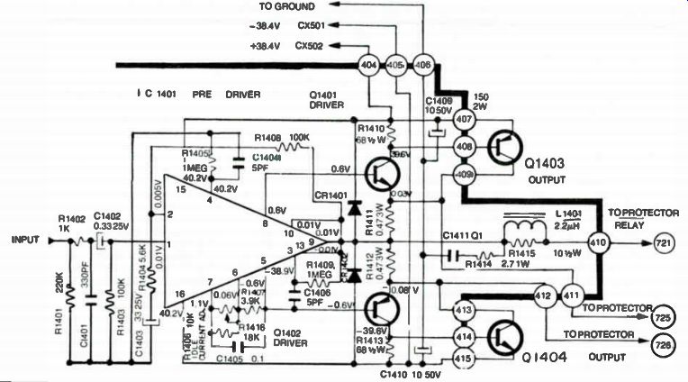
Fig. 14. Audio amplifier output circuit (IC).
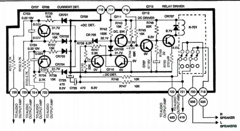
Fig. 15. Automatic speaker protection circuit.
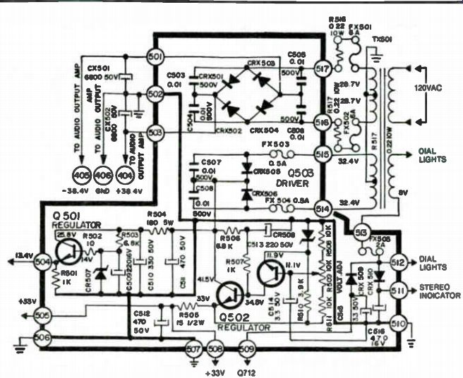
Fig. 16. Stereo receiver power supply circuit.
Two power supply sections are used for the amplifier circuit covered previously. These two power supply circuits are shown in Fig. 16. One supply is a full-wave bridge rectifier which is used to develop the split voltage required for the audio output stages. The second supply uses a full-wave rectifier with two regulator circuits. One regulator powers the RF/FM/multiplex circuits, while the second regulator (with voltage adjustment R509) powers the magnetic stereo cartridge and stereo pre-amplifier circuits that are used in another section of this system.
STEREO PUSH/PULL AMPLIFIER CIRCUITS
Stereo power amplifiers use push-pull arrangements primarily to minimize distortion. The push-pull circuit is most economical when high output power is required. Because the two halves of an ideal push-pull amplifier are perfectly balanced, the second harmonics are reduced and only the third and higher odd harmonics are of significance. This characteristic gives this type of circuit a major advantage in regard to overall distortion.
The low output impedance of transistors makes it possible to feed low-impedance loads directly. Because of this transistor characteristic, no matching device is required between the output transistor and the load, which is the speakers. Push-pull circuits can be classed as complementary and the quasi-complementary transistor amplifiers.
COMPLEMENTARY TRANSISTOR AMPLIFIERS
The complementary transistor is based on two elementary circuits.
This is the Darlington and the complementary pair of transistors.
Complementary amplifiers are produced when NPN and PNP transistors are used in series. Both the Darlington amplifier and the complementary pair are usable in individual push-pull circuits. These are shown in Figs. 17 and 18. In push-pull amplifiers, one output transistor conducts during the positive portion of the cycle and the second transistor conducts during the negative portion.
In Figs. 17 and 18, both amplifiers are directly coupled to each other. In Fig. 17, the input signal is first amplified by Q1 and fed to the two Darlington pairs. The transistors in the upper Darlington pair are NPN. They will conduct when the signal at the output of Q1 is in the positive portion of the cycle. The PNP transistors in the lower Darlington circuit will conduct during the negative portion of the cycle. Both portions of the cycle are put back together as a complete cycle across the load resistor.
Complementary pairs have been substituted for the Darlington circuits in Fig. 18. Basically, amplifiers using both types of circuitry behave more or less the same. Voltage for the bias circuit of transistors Q2 and Q3 is developed across RX2. Special diodes are frequently substituted for this resistor to improve bias stability, with temperature variations. A similar method is used for stabilizing a single-ended amplifier by the use of a diode in the bias circuit. In the collector of Q1, the load is the series combination of resistors, RX2, RB2 and RB3. One resistor, of a value equal to the two resistors, RB2 and RB3, would have done the job, but two resistors were used in order to connect a capacitor at their junctions. This capacitor is needed to overcome some circuit drawbacks.
Class B amplifiers, and to a lesser degree Class AB amplifiers, are prone to have distortion. Push-pull circuits are usually operated Class AB to reduce crossover distortion. In theory, when the upper transistor of Fig. 17 stops conducting in the class B mode of operation, the lower devices start conducting. However, there can be an instant in the cycle when the output transistors are not conducting. This characteristic causes what is known as crossover distortion. Considerable negative feedback is generally required in the circuit to eliminate or minimize the distortion.
Negative feedback is accomplished by having the RFB-CFB network feed the signal back from the output to the input circuit.
In order to accommodate large amounts of feedback, the amplifier must have high gain. Capacitor C provides positive feedback in what is referred to as a bootstrap circuit. Positive feedback increases the input impedance of Q2 so that the load in the collector of Q1 is large. This large collector resistance is necessary if Q1 is to have high voltage gain.
This capacitor, C, serves a second very important function. Should the positive peak in the signal be large, it places the base and emitter of Q2 at the same +Vcc potential. Transistor Q2 then will be cut off at the peak in the signal. C comes to the rescue by being charged when the circuit is idling. The voltage developed across C will maintain the base positive with respect to the emitter at all times, even during positive peaks in the cycle.
The transistor Q2, consequently, will not be turned off.
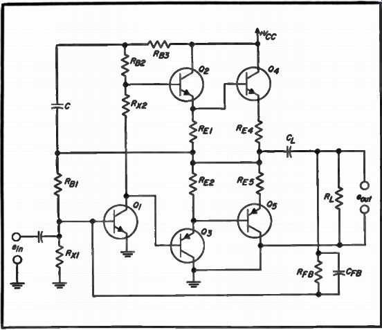
Fig. 17. Darlington pairs used in audio output circuit.
STEREO AMPLIFIER TROUBLESHOOTING
You may find that the troubleshooting of stereo amplifiers and FM multiplex systems can be greatly simplified by using a dual-trace oscilloscope and a square-wave audio or function generator. One such scope, shown in Fig. 19, is the SENCORE dual-trace Wide Bander model SC60. It will do a good job troubleshooting stereo amplifiers and many other electronic devices.
Brief Procedure Tips The basic concept of this test technique is to compare the normal operative channel with the inoperative stereo channel. Thus, one channel has to be operating properly. The square-wave audio signal is fed into both channels and the dual-trace scope is used to check and compare each channel's test points throughout all of the stages until the fault is located.
Of course, initial tests are performed for such obvious defects as excessive current drain, overheated solid-state devices, burnt resistors, poor solder connections, and cracked or broken circuit boards. Generally, after the preceding tests are performed and any faults corrected, at least one channel of the stereo system will be operating.
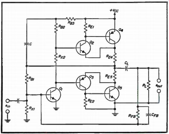
Fig. 18. Audio output circuit using complementary pairs.
Stage Gain Checks
Since the scope's vertical amplifier gain controls on triggered-sweep, dual-trace instruments are calibrated in volts percentimeter, and have matched vertical channels, it's very easy to check from one test point to another, to compare the signal gain of each stage, and make a comparison check of the right and left stereo channels. With this technique you can quickly isolate the amplifier trouble in the defective stage and almost to the very component.
As a final check of the amplifier, or if the original symptom was for insufficient frequency response, the function generators audio test frequency can be tuned throughout the entire audio range for a response check. Make these checks at 5 kHz intervals and look at the dual-trace scope patterns for both speakers at the same time.
Intermittent Trouble Location Hints
This technique will help you locate those pesky intermittent troubles in a stereo amplifier. In some cases, the volume level may go up and down intermittently, go out completely, or it may operate for hours before acting up at all. The method I have found useful is to inject a square-wave signal into the suspected channel and connect both scope probes to different stages of the amplifier. When the volume fluctuates or some noise occurs, just glance at the scope screen and take note of any changes in the waveshapes. If there is no change in the pattern, move the probes to different stages and make some more checks. With this technique you can isolate the defective stage or component quite rapidly.
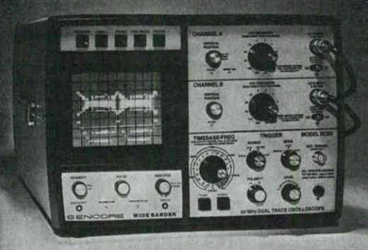
Fig. 19. SENCORE model SC60 dual-trace oscilloscope.