AMAZON multi-meters discounts AMAZON oscilloscope discounts
Transistor circuits for a wide range of applications are discussed in this guide, along with many different diode and transistor types. The most widely used circuit symbols are also shown ( see Fig. 1 ) , and each is discussed in detail in later sections of the guide. The common names are given in this figure; however, several manufacturers have adopted special names for their own products. For example, the silicon-controlled switch is known as a Thyristor by RCA and by Bell Laboratories, while Westinghouse calls it a Trinistor.
In addition to the different types of transistors, some thirteen different ways of forming them are shown in Fig. 2. All of these semiconductor devices have one purpose--to produce certain characteristics which can be used to advantage in specific applications. In some cases a transistor is named for the process by which it is made.
TRANSISTOR TYPES
Some basic transistor circuits are shown in Fig. 3. These are the common emitter, common base, and common collector. They are somewhat analogous to the grounded-cathode, -grid, and -plate of vacuum tubes. Transistors, because of their low impedance, are current-operated devices, whereas vacuum tubes are voltage operated because they are high-impedance devices.
A special form of solid-state device, the field-effect transistor, can be considered a stepping stone between a vacuum tube ( which is voltage-operated) and a transistor ( which is current operated). Fig. 4A is a schematic of a field-effect transistor. The unit consists of an N-type silicon bar with two ohmic contacts-a cathode at one end and an anode at the other. Two PN junctions are built into the middle, and are connected in parallel to serve as the grid.
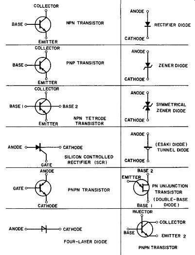
Fig. 1 - Transistor circuit symbols.
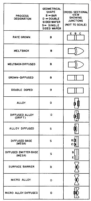
Fig. 2 - Transistor forms.
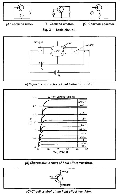
Fig. 3 - Basic circuits.
Fig. 4 - Transistor types.
A negative bias applied to the grid increases the effective resistance between the anode and cathode, producing a triode output characteristic. As the anode voltage is increased, a voltage drop develops across the grid junctions, causing them to become reverse-biased. At some point, a further increase in anode voltage will not appreciably increase the anode current. As a result, the output characteristics of the unit closely resemble those of the vacuum-tube pentode.
The anode potential at which anode-current saturation occurs is known as the pinch-off voltage. Anode current flowing through the device after the pinch-off voltage has been reached is called the pinch-off current. With zero grid bias, the pinch-off current is the maximum specified anode current. The transistor is in the triode region before pinch-off occurs, and in the pentode region after the pinch-off potential has been reached. This may be seen from the characteristic chart in Fig 4B. Below an anode voltage of about 10 volts, the operational curves resemble those of a triode; to the right they are similar to those of a pentode. Part C shows the circuit symbol of the field-effect transistor. Unlike a tube, the anode and cathode terminals are interchangeable, although a somewhat higher transconductance and lower noise figure is generally obtained by using the unit in the normal way.
The grid normally requires a negative potential. Positive bias on the grid will increase the anode current, but should remain below 0.6 volt. Otherwise, substantial grid currents-capable of destroying the device-will develop.
Except for lower anode voltages, field-effect transistors used as amplifiers have the same circuitry as triodes and pentodes. The polarities of the applied voltages are also the same.
COMPOSITE TRANSISTORS
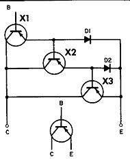
Fig. 5 - Composite transistor equivalent circuit.
Packaged amplifiers with gains of up to 30,000 are available in the form of composite transistors. A typical PNP unit, the 2Nl161, has a collector voltage of 30 volts with a current of up to 3 amperes. Maximum dissipation is about 50 watts, and the current gain goes as high as 10,000. Beta (B )-or the current gain when the transistor is used as an amplifier in a common-emitter configuration-usually is less than 300 to 400, although some composite transistors have betas of up to 30,000. The drawing in Fig. 5 shows the equivalent circuit. As in a single transistor, there are three external terminals-C, B, and E-corresponding to the collector, base, and emitter. In effect, the composite transistor appears as a low-power amplifier at the input and a high-power unit at the output. The betas multiply, and the total beta for Fig. 5 would be Bl·B2·B3. However, the diode shunts absorb some of the base-emitter currents as thermal compensation.
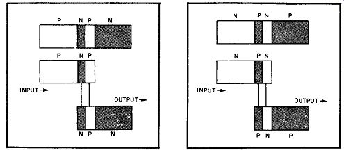
Fig. 6 - Hook transistor (PNN).
Fig. 7 - Hook transistor (NPP).
(A) Equivalent circuit. (B) Junctions shown.

Fig. 8 - Controlled switch.
FOUR-ELEMENT DEVICES
Some of these units are hook transistors, which are PNN or NPP devices. A PNN unit has three junctions, as shown in Fig. 6.
As redrawn, a hook transistor appears as a PNP to the input and an NPN to the output. An NPP unit ( Fig. 7) is the reverse of a PNN. Controlled Switch The controlled switch or CS ( like the silicon-controlled rectifier) is another PNPN device. The CS is related to the controlled rectifier ( SCR) in both physical construction and theory of operation, but has a much greater firing sensitivity. It is therefore useful in many low-level input applications outside the capability of controlled rectifiers.
Consider two transistors connected together as in Fig. 8A, one a PNP and the other an NPN. Electrode A (anode) is attached to the upper P region, C (cathode) connects to the lower N region, and a third electrode (gate) goes to the P region of the NPN triode. Actually, as shown in Fig. 8B, there are only four regions in a single wafer, with three junctions. Electrically, the transistor pair appears as shown in Fig. 9A, while 9B shows the schematic symbol for the CS. In operation the collector of X2 drives the base of X1, and the collector of X1 drives the base of X2. Where beta Beta 1is the current gain of X1, and Beta 2 the current gain of X2, the gain of this positive-feedback loop is their product, beta 1 X beta 2 = beta 3.
Where beta 3 is less than 1, the circuit will be stable; otherwise, it will be regenerative. With a small negative current applied to terminal G, the NPN transistor is biased off and loop gain is less than unity ( 1). The only current that can flow between output terminals A and C is the cutoff collector current of the two transistors, and the impedance between A and C is very high at this time.
(A) Transistor equivalent. (B)Schematic symbol.
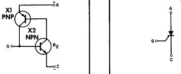
Fig. 9 - Controlled switch.
When a positive current is applied to terminal G, the NPN transistor is biased on, causing its collector current to rise. Since the current gain of the NPN, beta 1, increases with the collector current, a point is reached where loop gain equals unity and the circuit becomes regenerative.
Collector current of the two transistors rapidly increases to a value limited only by the external circuit. Both transistors are driven into saturation, and the impedance between A and C be comes very low. In this state, the positive current which was applied to terminal G to trigger the self-regenerative action is no longer required, since the collector of the PNP supplied more than enough current to drive the base of the NPN. The CS circuit will remain on until turned off by reducing the collector current below the value necessary to keep beta 3 at or above unity.
Trigistor
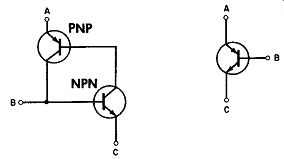
Fig. 10 - PNPN trigistor and dyna-quad.
(A) Bistable circuit. (B)Conventional transistor circuit.
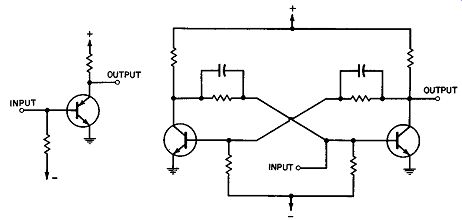
Fig. 11 - Trigistor and transistor circuits.
Another PNPN device of similar construction is the silicon Trigistor ( Fig. 10). This is a semiconductor component with characteristics which allow it to approximate the circuit function of a flip-flop or bistable multivibrator. It is also known as a Dyna quad, a PNPN device with the unique property of trigger control turn-off and turn-on at its base.
The Trigistor will turn on whenever a low positive trigger pulse is applied to its base; it will remain on without a sustaining base current. A negative trigger pulse applied to the base will turn it off, and keep it off until triggered on again. The circuit will then remain on until triggered off by a negative current pulse at terminal B, which diverts the collector current of the PNP from the base of the NPN. Since regenerative action is no longer sustained, the two transistors return to their stable cutoff condition.
Fig. 11A illustrates the inherent simplicity of a Trigistor bi stable circuit. A conventional transistor flip-flop is shown in Fig. 11B for comparison. Trigistor switching circuits require fewer components than do transistors or other switching elements. Normally, one Trigistor will perform the same function as two transistors plus several associated capacitors and resistors.
The Trigistor is turned off by a gate signal. In the controlled switch (CS) and silicon-controlled rectifier ( SCR), the gate turns the device on, and lowering the collector voltage turns it off.
The CS is inherently a highly sensitive device because the in put NPN transistor is designed with high gain. It is therefore useful for high-gain switching directly from low-level control signals. Usually no intermediate stages of amplification are needed in the control circuits.
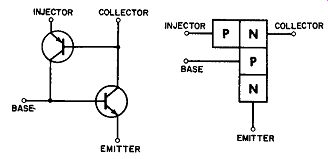
Fig. 12 - Binistor equivalent circuit.
Where high sensitivity is not required or desired, any degree of reduced sensitivity can be achieved by biasing the gate. In fact, some negative gate bias is recommended for all circuits, to insure absolute "no-fire" stability. Since the CS has a very high gain, it should not be operated or tested with the gate open.
For many applications, stabilizing bias is easily achieved by adding a resistor between the gate and cathode. The resistance is determined by the maximum operating temperature for the application. Since biasing reduces the firing sensitivity, the correct resistance is a key part of circuit design.
The Binistor
The Binistor is another PNPN device. Of the many four-layer devices available, it represents a new mode of operation offering many advantages over more usual techniques. Its negative-resistance characteristics, usually determined by internal parameters in conventional four-layer devices, are determined instead by the external circuitry. The result is stable operation over wide temperature limits.
The two-transistor equivalent circuit of the Binistor is shown in Fig. 12. Although all electrodes may be used as inputs, the most interesting performance is obtained when the collector is considered an output and the base an input, with the injector providing the "latching" current required for bi-stability. The injector may also be used to switch the Binistor off in certain circuits.
If base current is applied, then normal transistor action will cause the collector voltage to fall. When it drops below the injector clamp voltage, the upper PN junction will become forward biased and injector current will begin to flow in such a direction that it helps the NPN transistor switch on. Hence, a regenerative action takes place that tends to drive both transistors into the saturated "on" state. No further external base current is required to maintain the Binistor in this condition, the base current for the NPN transistor being supplied by the injector circuit.
Switch-off can be achieved either at the injector or, with certain Binistor types, at the base. If the injector current is reduced to the point where the base current of the NPN section is insufficient to keep the Binistor in saturation, the collector voltage will rise. When it goes above the injector clamp voltage, the upper PN junction will become reverse-biased and regeneration will complete the switch-off. Therefore, the criterion for switch-on is that the collector voltage be taken below the injector clamp voltage. Conversely, for switch-off the collector voltage must be taken above the injector clamp voltage.
PNPN Diode
(A) Four-layer diode. (B) Load switch. (C) Voltage-current characteristics.
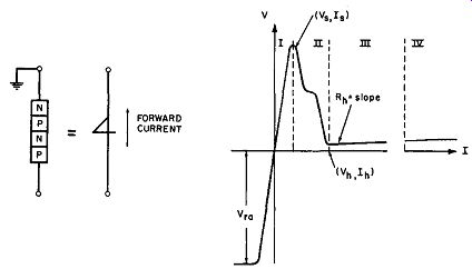
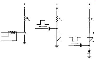
Fig. 13 - PNPN diode.
The PNPN four-layer diode in Fig. 13A is a two-terminal, self actuated silicon switch with operating characteristics based on the principles of transistor action. It has two stable states-an "open", or high-resistance, state of more than one megohm; and a "closed", or low-resistance state, of just a few ohms. It is switched from one state to the other by controlling the voltage across it and the current through it.
Because of its characteristics, this four-layer diode can serve as a load switch ( Fig. 13B). A positive pulse on its anode or a negative pulse on its cathode will start and then sustain conduction.
The voltage-current characteristic for the four-layer transistor diode shows the four essential operating regions ( see Fig. 13C).
These are the open, or high-resistance; transition, or negative resistance; closed, or low-resistance; and high-pulse current states.
When B+ is applied, the voltage across the diode rises to the point where it switches the unit to the closed state. ( Switching occurs because an internal-feedback mechanism allows the diode to pass a steadily increasing current when the voltage is held at a fixed value. ) The current in the closed state is less than 200 µ.a; therefore, the transistor diode will pass the required current.
In the closed state, the device has a resistance of only a few ohms. As long as the circuit passes sufficient current, the closed, or "on," condition will be maintained. At the point marked "VH" on the curve, the circuit is passing just enough current to keep the device in the closed state. If the current drops below this point, the diode will switch back to its high-resistance, or "off," condition.
Prior to switching, the reverse-biased junction of the four layer transistor diode acts as a capacitor. It is necessary to charge this capacitor as well as to inject current carriers into it during switching. The energy required must be furnished either by a trigger pulse or by circuit elements provided for this purpose.
Usually a .002-mfd capacitor or higher is added from the positive terminal to ground.
The switching characteristic of the transistor diode is deter mined by the "on" and "off" time constants, and the circuit will determine the actual switching time. The higher the trigger voltage applied and the faster it rises, the faster the unit switches.
Diodes are available with switching voltages from 20 to 200 volts and holding currents of 1 to 50 ma. Within these limits, a series of standard ranges with specific tolerances makes it possible to select units with characteristics meeting specific needs.
The transistor diode will turn off when the current through it is below the holding current. The speed of this turn-off depends on circuit conditions. In a typical sawtooth oscillator, for example, the device must turn off while holding voltage is applied.
This will normally take about one microsecond.
In its "off" condition, the transistor diode may be considered a capacitance and large resistance in parallel. This capacitance is similar to the collector capacitance of a normal transistor, but its value depends on the actual voltage across the device. In its "on" condition, the transistor diode has such a low resistance that capacitive effects may be ignored. In its "off" condition, capacitance current will pass in response to a sharply rising voltage wave. If this voltage wave rises fast enough, switching will occur below the DC switching voltage.
Since its resistance decreases as the current increases ( to substantially less than 1 ohm at high pulse currents), the diode can be destroyed unless the load current is limited. To switch the diode on, the series impedance should pass more than the value of holding current.
SPECIAL DIODES
Silicon diodes are used for rectifiers where, with a positive anode or negative cathode, they conduct in the forward direction.
A typical operating curve is shown in Fig. 14A. If a small reverse voltage is applied, the current flow will be in microamperes, rather than milliamperes as in the forward direction. The germanium diode, in contrast, does not have as sharp a front-to-back ratio, although it does conduct more heavily in the forward than in the reverse direction ( see Fig. 14B). Zener Diodes When a reverse voltage is applied to the silicon diode, however, it breaks down at a certain point. This sharply defined potential is the zener, or breakdown, voltage. At this point the silicon diode conducts, much like a gas tube. The breakdown does not damage the silicon diode, and it recovers when the re verse voltage is removed.
The important feature is that, at breakdown, the voltage is almost independent of the amount of current flow. Thus, the diode acts as a voltage regulator, maintaining a constant voltage drop over a wide current range.
(A) Silicon diode operating curve. (B)Germanium diode operating curve.
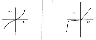
Fig. 14 - Special diodes.
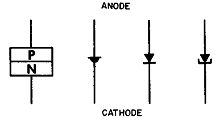
Fig. 15 - Tunnel diode circuit symbols.
Silicon diodes designed for this use are called zener types and are designed for specific zener voltages. They are used for voltage regulation and reference. Other silicon diodes used as rectifiers have such high zener voltages that these voltages are rarely reached. Consequently the diode does not break down under normal inverse-voltage conditions.
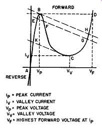
Fig. 16 - Tunnel diode characteristic curve.
Tunnel (Esaki) Diode
The tunnel diode is a fairly new semiconductor device with wide potential as an amplifier, switch, or oscillator. It can be made from either germanium or silicon, and can be identified in a circuit diagram from any of the three symbols in Fig. 15.
Ordinary transistors ( and even vacuum tubes) depend on current carriers being influenced by the potential between the emitter and collector electrodes. Carrier speed therefore is limited by the time required for them to travel through these regions.
Tunnel diodes, however, operate on a different principle, and their theoretical frequency limit of 10^7 megacycles is much higher than that of any other semiconductor device.
The tunnel diode, so called because of its tunnel effect, operates on the principle of quantum theory whereby a particle can disappear from one side of a potential barrier and instantly re appear on the other side-even though it apparently does not have enough energy to overcome the barrier.
As shown by the characteristic curve in Fig. 16, as voltage is applied to the diode, current rises sharply to a peak. If the applied forward voltage is further increased, the current dips sharply and then rises again to its original peak and even higher. Peak currents can be anywhere from only a few microamperes to well into the ampere region.
The negative-resistance region following the first current peak makes the tunnel diode useful as an active circuit device. In addition, a tunnel diode has an extremely low impedance in the re versed-biased state, and a normal diode characteristic at high forward voltages ( operating along the second current peak). The two most common uses for tunnel diodes are as switches ( where the unit is switched from a low- to a high-voltage positive resistance state), and in linear amplifiers and oscillator circuits ( where it is biased in the negative-resistance region). For bistable operation, positive-resistance sections of the characteristic curve are used ( current increases with voltage). Referring again to Fig. 16, points A and B (both positive-resistance points) are connected to produce a load line for bistable operation. Point A is a high-voltage, low-current point and B is a low voltage, high-current point. Each represents a stable state for the tunnel diode. If the diode is biased at A and a trigger pulse is applied to increase the current, the diode will switch to its low-voltage state. Removing the trigger will return the diode to its high voltage, or second stable, state.
Backward Diodes
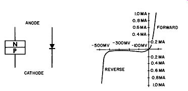
Fig. 17-- Backward diode and characteristics curve.
In manufacturing, it is possible to eliminate the peak in the forward characteristic of a tunnel diode. With signals smaller than about 400 mv (in a typical germanium diode), the "reverse" quadrant exhibits the low impedance and the "forward" quadrant the high impedance. This, then, is the "backward" diode. A typical characteristic curve is shown in Fig. 17.
Typical applications for the backward diode are in tunnel diode circuits as a uni-lateralization element, and in detection or low-voltage reference circuits. When the backward diode is biased in the low-impedance direction (reverse-biased), diode action is entirely due to majority current. Recovery time is therefore not limited by any stored-charge phenomena.