Fig.2.1 A conventional stereo volume and balance control circuit
| Home | Audio mag. | Stereo Review mag. | High Fidelity mag. | AE/AA mag. |
In this second section we will mainly be concerned with filter circuits, such as tone controls, and scratch and rumble filters.
Some other audio preamplifier related topics are also considered. such as audio level limiting, and audio mixing.
Mono to Stereo
One of the more commonly asked questions when audio power amplifier designs are published is "how do I produce a stereo version of the amplifier"? The simple answer is that you build two of them, one for each stereo channel. I suppose that in truth this is a slight over-simplification, since the two power amplifier modules are normally united via a common volume control and balance control.
The most simple form of volume and balance control is the type which uses a dual concentric potentiometer. This is basically just a dual gang potentiometer with one section used as the volume control for the left channel, and the other connected as the volume control for the right hand channel. The two gangs are controlled via separate but concentric control knobs which are easily adjusted in unison. However, there is no difficulty in holding one knob still while moving the other, so that the two volume levels can be set for an accurate balance. This method is quite a good one, but it seems to be far more common on stereo cassette decks than on stereo power amplifiers. For the home constructor it has the advantage of being simple and straightforward, but the disadvantage that suitable components tend to be very difficult to obtain.
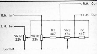
Most stereo power amplifiers have a common volume control which uses an ordinary twin gang potentiometer. Channel balancing is effected by a separate control, which in most cases is a single gang potentiometer. Figure 2.1 shows the circuit diagram for a volume and balance control of this type.
VR1a and VR1b are the standard stereo volume control, with one gang connected in each channel. The two output signals are taken via series resistors R1 and R2, and there will be small losses due to the voltage drops through these resistors.
Fig.2.1 A conventional stereo volume and balance control circuit
We are assuming here that the circuit feeds into a reasonably high load impedance of several kilohms or more. If the circuit feeds into a lower impedance, it will only work well if a buffer amplifier is used to reduce the loading on the output.
We are also assuming here that VR2 is set at a roughly mid-setting. It then introduces relatively small signal losses due to the potential divider action with R1 and R2.
Moving the wiper of VR2 well towards the left end of its track produces large losses through R1 due to the low resistance through VR2 to earth. Taking the wiper fully to the left hand end of the track actually short circuits the output from R1 to earth, and cuts off the signal completely. It has the opposite effect on the signal through R2, which is connected to earth through the full resistance of VR2, causing minimal losses. Taking the wiper of VR2 to the other end of its track produces minimal losses through R1, but produces large losses through R2. Again, taking the wiper right to the end of the track cuts off the signal completely. However, it is the left hand signal that is cut off this time.
Therefore, by adjusting VR2 it is possible to have the left hand signal only, the right hand signal only, or a mixture of the two at any desired relative levels. This enables the correct channel balance to be obtained even if there are factors that cause a strong innate imbalance in the system. In practice quite large channel imbalances are not uncommon. Remember that even sitting a bit closer to one loudspeaker than to the other can severely upset the perceived balance of the system.
Obviously construction of a volume and balance control circuit should give no major problems. The circuit can easily be hard-wired, but try to keep the wiring as short as possible so that stray pick-up is kept to a low level. Normally the volume and balance controls arc connected at the inputs of the power amplifiers. As the signal levels here tend to be quite high but the impedances do not, stray pick-up is not likely to be a major problem. You obviously need to take care when wiring up VR2, so that the balance control operates in the logical manner (clockwise rotation boosts the right hand channel - counter-clockwise rotation boosts the left hand channel).
Components for Figure 2.1 Resistors (all 0.25 watt 5% carbon film)
R1 4k7 R2 4k7
Potentiometers
VR1 VR2 22k log carbon dual gang 47k lin carbon
Miscellaneous
Two control knobs, wire, etc.
There is an alternative type of balance control which is sometimes used. Figure 2.2 shows the circuit for a control of this type. VR1 is a dual gang potentiometer connected in what is almost a conventional stereo volume control circuit.
It differs from the normal volume control connection only in that the two gangs are connected in anti-phase. In other words, as one is adjusted for higher gain, the other is set for reduced gain. The potentiometer should be a linear type so that there is a loss of 6dB through each channel at the central setting (a logarithmic type would give unequal losses at the central setting).
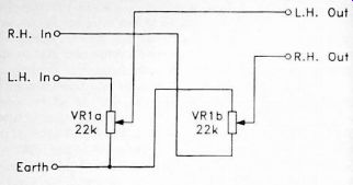
Fig.2.2 An alternative form of balance control. VR 1 is a dual gang linear
type.
This type of balance control is in some ways a neater solution to the problem, but the loss of around 6dB through the circuit is somewhat higher than the typical signal loss through the type described previously. This is not a major signal loss though, and can usually be made up quite easily by boosting the gain of the preamplifier stage or stages. Alternatively the circuit can be followed by an amplifier having a voltage gain of about 6dB to compensate for the losses.
Audio Limiter
If a power amplifier should become seriously overloaded the result is severe clipping of the output signal. This has a disastrous affect on the output quality, with high levels of distortion being produced. The distortion products tend to be at high frequencies, and produce a pretty unpleasant sound. There is also a risk of damage to the tweeters in multi-way loudspeaker, systems. The high frequency drivers are normally designed to handle only relatively modest power levels, but with a clipped signal they will receive much higher power levels than normal. This can result in the voice-coil burning out.
One way to ensure that problems with overloading can not occur is to add an audio limiter at the input of the power amplifier. This is a circuit which normally lets the audio signal pass straight through to the power amplifier, but which will reduce the signal level if it exceeds a certain threshold figure. Ideally it should cut back the gain by amounts which keep the output level constant when an overload occurs.
Practical limiter circuits permit some increase in the output level as the input is increased beyond the threshold level, but by only a small amount. If the threshold level is made slightly lower than the maximum input voltage required by the amplifier, overloading will not occur even if a grossly excessive input level is applied to the limiter. On the other hand, ordinary input signals can drive the amplifier to output powers that are very close to the maximum it can provide.
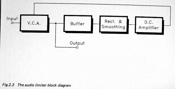
Figure 2.3
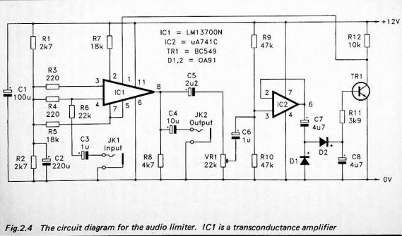
Figure 2.4
The block diagram of Figure 2.3 shows the arrangement used in a conventional audio limiter. The circuit is based on a voltage controlled attenuator (v.c.a.). This normally allows the input signal to pass through to the output with minimal losses. Its gain can be controlled by means of a d.c. voltage though, and by reducing this control voltage the losses through the circuit can be greatly increased.
In this case the control voltage is provided by a form of d.c. amplifier which normally has a high output voltage. This gives the required low losses through the v.c.a. under standby conditions. The input signal for the d.c. amplifier is derived from the output signal via a buffer stage, and a rectifier plus smoothing network. The buffer stage prevents the non-linear loading of the rectifier from producing distortion on the output signal.
The rectifier and smoothing circuit produces a positive d.c. bias that is roughly proportional to the strength of the output signal. Small bias levels have no affect on the d.c. amplifier, but above a certain point only a minor increase in the input level produces a large reduction in the output voltage. Therefore, above a certain output level, the gain of the v.c.a. reduces substantially if the output level is increased. This gives a form of negative feedback action which tends to stabilize the output signal at the threshold level, provided the input level is high enough.
Figure 2.4 shows the circuit diagram for the audio limiter unit. This is based on an operational transconductance amplifier (IC1), which differs substantially from an ordinary operational amplifier. The main difference is that it is a current operated device, and not a voltage activated type. It has the usual differential inputs (pins 3 and 4), but these respond to the difference in the input currents. By using a series resistor at an input, the input current flow through the resistor becomes proportional to the applied voltage, effectively converting the input to a voltage operated type. This is the purpose of R6.
The output from the device is a current rather than a voltage, but by adding a load resistor the current flow is converted into a proportional output voltage. R5 is the output load resistor. Another respect in which a transconductance amplifier is radically different to an ordinary operational amplifier is that it has a control current input (pin 1). The output current is a function of the differential input current and this control current. In practice this means that the gain of the device can be controlled via the control current, and is proportional to it. In this case the control current is provided by R12, which also acts as the load resistor for TR1. By switching on TR1 some or all of the control current can be diverted, and the gain of IC1 can be greatly reduced.
R1, R2, and C2 provide a center tap on the supply lines which is used for bias purposes. R7 provides a bias current to the linearizing diodes in IC1. This helps to give low distortion at high input signal levels. The output impedance of the transconductance amplifier is quite high, but the LM13700N used for IC1 has a built-in output buffer amplifier. R8 acts as the output load resistor for this stage. There is no negative feedback network incidentally. Transconductance amplifiers are normally used open loop (as in this case), or with only a very small amount of negative feedback.
Some of the output signal is coupled to buffer amplifier IC2 via variable attenuator VR1. From here the signal is fed to a conventional rectifier and smoothing circuit based on D1 and D2. Due to the threshold voltage of TR1, and the small voltage drops through the diodes, an output level of around 800 millivolts peak to peak is needed before TR1 will start to switch on. However, due to the low value of R11, an output voltage only slightly higher than this will cause TR1 to be biased virtually into saturation, giving around 90dB of attenuation through the v.c.a.
This well defined threshold point helps to give the circuit a very good limiting characteristic, rather than simply having it apply dynamic compression across a wide range of input levels. Figure 2.5 shows the limiting characteristic for the prototype circuit. This is with VR1 set for zero attenuation.
If VR1 is backed-off slightly, a higher output level is needed in order to bring TR1 into conduction. VR1 can therefore be used to raise the limiting threshold level to any desired voltage (within reason) above the basic 800 millivolts peak to peak threshold level.
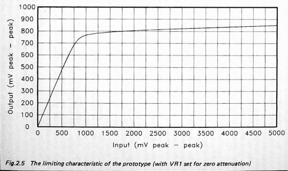
Fig. 2.5
I suppose that strictly speaking IC1 does not act as a voltage controlled attenuator. It is really a sort of buffer amplifier, but as its voltage gain is never more than about unity, and can be substantially less than unity, it provides a form of variable attenuator action. I suppose that it is not strictly a voltage controlled circuit either, as it is a bias current that controls its gain. However, this is largely of academic importance.
Construction of this project is very straightforward. The component layout is not critical because the gain of the circuit is only about unity or less, and the input impedance is not very high at around 22k. Instability and stray pick-up are not likely to be problems. One point worth mentioning is that D1 and D2 are germanium diodes, and not the more familiar silicon type. This means that they are vulnerable to heat damage, and due care should therefore be exercised when soldering them into circuit. It should not be necessary to use a heat-shunt provided the soldered joints are completed reasonably swiftly.
The voltage gain of the circuit is approximately unity up to the limiting threshold. If desired, the voltage gain can be boosted by making R6 lower in value, but this will reduce the input impedance of the circuit. The input impedance is roughly equal to the value of R6. If reduced gain is needed, simply make R6 higher in value (which will boost the input impedance). VR1 should be backed-off as far as possible without the amplifier becoming overloaded on excessive input levels. Back it off too far and the unit will not prevent overloading. Back it off too little and the power amplifier will never be driven at something approaching maximum output power. A little experimentation should soon locate a suitable setting. Try to avoid having the limiter almost continuously driven beyond its threshold level. This would result insignificant compression of the dynamic levels in the program material.
Although IC1 is shown as an LM13700N in the components list, the LM13600N is virtually identical and is also suitable. These days most electronic component retailers seem to supply the LM13700N though.
Components for Figure 2.4
Resistors (all 0.25 watt 5% carbon film)
R1 2k7 R2 2k7 R3 220R
220R R4 R5 18k R6 22k R7 18k R8 4k7 R9 47k R10 47k R11 3k9 R12 10k
Potentiometer VR1 22k sub-min preset
Capacitors
C1 100*1 25V elect 220u 25V elect 1u 63V elect 10u 50V elect 2p2 63V elect C2 C3 C4 C5
C6 1u 63V elect
4u7 63V elect
4u7 63V elect
C7 C8
Semiconductors
LM13700N or LM13600N MA74IC BC549 OA91 OA91 IC1 IC2 TR1 D1 D2
Miscellaneous standard jack socket standard jack socket 16p-in d.i.l. i.c. holder, 8 pin d.i.l. i.c. holder, case, circuit board, etc.
JK1 JK2
For stereo operation two sets of components are required, but obviously only one case of adequate size to accommodate everything is needed. Note that LM13700N actually contains two transconductance amplifiers and output buffer stages, and that it is possible to use one section in each stereo channel.
This list gives connection details for the second section of the device. The supply terminals (pins 6 and 11) are common to both sections incidentally.
Section 2 Pin No.
Section 1 Pin No.
Function 16 Control Input Diode Bias
+ input
- input
Amplifier Output Buffer Input Buffer Output 1 15 2 14 3 13 4 12 5 10 7 9 8
Scratch and Rumble
The quaintly named scratch and rumble filters are mainly designed for use in conjunction with record playing equipment.
Using good quality equipment and modern records there should actually be no need for either type of filtering. The background noise level should be low, with no "snap", "crackle", and "pop", or low frequency "clunks" and "rumbles". In the real world you will often be playing one of your favorite records from many years ago on something less than "state of the art" equipment.
Even well cared-for records tend to suffer from the effects of mild scratches and dust particles in the grooves over a period of time. The "hiss" level can also be quite high on older recordings, which were in many cases made from master recordings which had poor signal-to-noise ratios by modern standards. The low frequency noises can simply be due to inadequacies in the mechanism of the record deck. They can also be produced by warps and other mechanical problems with the record itself.
A scratch filter can be used to combat the high frequency noises, which includes both the "crackle" produced by small scratches and groove contamination, and ordinary "hiss" type noise. Opinions vary when it comes to choosing the best cut-off frequency and attenuation rate for this type of filter. It has to be a compromise between a low enough frequency to give good noise reduction, and a high enough frequency to prevent the audio quality from being degraded too far.
Similarly, the roll-off rate needs to be high enough to give good noise reduction, but it should not be so fast as to make the filtering too obvious. Using so called "brick wall" filtering it is possible to get some very impressive levels of "crackle" reduction, but to my ears at any rate, this type of scratch filtering sounds pretty terrible. There is a similar problem with the rumble filtering, where it would be possible to get some impressive results by completely eliminating all the bass signals! The scratch and rumble filters featured here both have an 18dB per octave roll-off rate. This is high enough to give a good degree of noise reduction, but it docs not make the addition of the filtering over-obvious. The cut-off frequency of the scratch filter is at about 7kHz. This obviously trims a fair amount off the upper part of the audio range, but it leaves a sufficient high frequency content for subjectively good results. Setting the cut-off frequency any higher is likely to give too little "crackle" reduction to make the addition of the filtering worthwhile. The rumble filter has a cut-off frequency of about 100Hz, which gives significant trimming of the bass frequency content. It retains a reasonable degree of fidelity though, and provides quite high attenuation of very low frequency and sub-audio noise.
Sub-audio noise may not seem to be a problem, as it is clearly inaudible. However, strong very low frequency signals, such as those produced by many warped records, can have audible effects. The main problem is that of the power amplifier's biasing and the loudspeaker cone effectively being varied from their normal central settings. This can cause clipping and severe distortion on one set of half cycles on strong signals.
Figure 2.6 shows the approximate frequency response of the prototype scratch and rumble filters. As will be explained more fully later on, you can easily alter the cut-off frequencies to suit individual requirements.
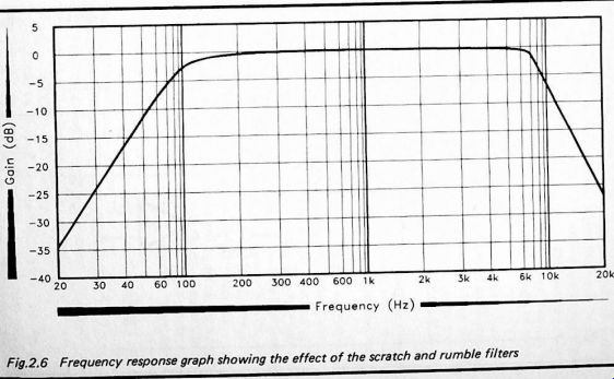
Figure 2.6
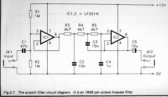
Figure 2.7
The Circuits
Taking the scratch filter circuit first (Fig.2.7), this is a conventional third order active circuit. Although it might seem that a three-stage passive C - R filter would have the desired effect, the performance of such a filter tends to be rather poor in a practical situation. One problem with passive filters is that they are dependent on being fed from a low source impedance, and feeding into a high load impedance. This makes it essential to have input and output buffer stages in order to obtain reliable and predictable results. In this case IC1 is the input buffer and IC2 acts as the buffer at the output of the circuit.
Active filtering goes beyond this simple buffering though, and positive feedback is used to enhance performance. In this circuit the feedback consists of having the bottom end of C3 connected to the output of IC2 instead of going to earth. If we ignore this fact for the moment, the circuit is just a three- stage passive affair. The first stage is formed by R3 and C2, while the next two stages are comprised of R4 and C3, and R5 plus C4.
The main problem with a passive filter is that it tends to introduce the filtering quite gradually, with the full attenuation rate only being achieved well past the break frequency.
The use of feedback can provide a much more abrupt introduction of the full attenuation rate. This avoids having a significant amount of attenuation well below the cut-off frequency in order to obtain the required amount of attenuation above the cut-off point.
At pass frequencies C3 has no effect. Any change in voltage at one end of the component is matched by an identical change at the other, giving no change in the charge voltage across C3. Below the cut-off frequency the situation is different, because the filtering provided by R5 and C4 means that the output signal will be smaller than the signal at the junction of R4 and R5. C3 then starts to provide filtering in conjunction with R4, and due to the relatively high value of C3, it provides quite strong filtering. This gives the required abrupt introduction of the filtering.
The explanation given above is a slight over-simplification, and with active filters such as this the circuit values have to be selected quite carefully. An error in one direction and the filtering is not much different to a passive design. An error in the opposite direction and the response can have a pronounced "hump" just below the cut-off frequency. In fact, in an extreme case the circuit can "ring", or actually break into oscillation at approximately the cut-off frequency. In an application of this type it is usually best to err on the safe side, and have a response that is completely free from resonances, even if this does result in the attenuation being introduced slightly less abruptly. As can be seen from the response curve of Figure 2.6, these filters are "hump" free.
The rumble filter circuit appears in Figure 2.8. This is much the same as the scratch filter, but resistors and capacitors in the filter network have been swopped over so that a highpass rather than a lowpass filter action is obtained. Also, the component values have obviously been changed to suit the required 100Hz cut-off frequency.
Construction of these circuits should present no real problems as they have only about unity voltage gain. Therefore, there is no real danger of instability. The circuit should be added ahead of the power amplifier (not ahead of a preamplifier), where it will handle quite high signal levels. Stray pickup should not therefore be a major problem either.
When using filters of this type you should bear in mind that they are just simple filters, and that they can not work miracles! The scratch filter should be very effective against high frequency "hiss", and "clicks" produced by minor scratches and small dust particles. It can not combat large scratches as these produce signals over a wide range of frequencies, going well down into the audio range. A proper noise blanker is the only effective way of combating severe scratches, and this is a relatively complex piece of equipment.
It certainly goes well beyond the scope of this guide. The rumble filter should be very effective against low frequency audio and sub-audio noise. It can not be expected to combat the noise from some very cheap record decks which is predominantly at relatively high frequencies.
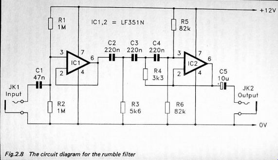
Figure 2.8
Components for Figure 2.7
Resistors (all 0.25 watt 5% carbon film) R1 1M R2 1M R3 4k7 R4 4k7 R5 4k7
Capacitors C1 47n polyester 10n polyester 5% or better 15n polyester 5% or better 1 n polyester 5% or better 10u 50V elect C2 C3 C4 C5
Semiconductors IC1 LF351N
LF351N IC2
Miscellaneous standard jack socket JK1
standard jack socket Case, circuit board, two 8 pin d.i.l. i.c. holders, wire, solder, etc.
JK2 Note that for stereo operation two sets of components are required, but obviously only one case of adequate dimensions to accommodate both circuit boards is needed.
Components for Figure 2.8
Resistors (all 0.25 watt 5% carbon film) R1 1M R2 1M 5k6 R3 3k3 R4 R5 82k R6 82k
Capacitors C1 47n polyester 220n polyester 5% or better 220n polyester 5% or better 220n polyester 5% or better 10u 50V elect C2 C3 C4 C5 Semiconductors IC1 LF351N
LF351N IC2
Miscellaneous JK1 standard jack socket standard jack socket
Case, circuit board, two 8 pin d.i.l. i.c. holders, wire, solder, etc.
JK2
Note that for stereo operation two sets of components are required, but obviously only one case of adequate dimensions to accommodate both circuit boards is needed.
Switching
Neither the scratch or the rumble filters will be needed all the time, and some means of switching out the filtering will therefore be needed. The most simple method is to use an s.p.s.t. switch connected as shown in Figure 2.9. This shows the...
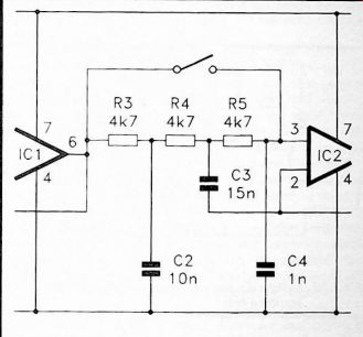
Fig.2.9 An s.p.s.t. switch can be used to provide a means of switching out
the filtering
... switch added to the scratch filter, but the same method of connection will work with the rumble filter (i.e. add the switch between IC1 pin 6 and IC2 pin 3). The additional switch leaves the circuit to function normally when left in the open position. When it is closed it bypasses the filter components and removes the filtering. This leaves some frequency dependant loading on the buffer amplifiers, but their low output impedances should prevent this from having any unwanted effects.
The alternative, and slightly better approach, is to use a d.p.d.t. switch to bypass the entire filter circuit when it is not required. Figure 2.10 shows the correct method of connection for the switch. This has the advantage of removing any slight noise and distortion generated by the filter when it is not in use.
Filter Circuit
A A Sib S1 Q
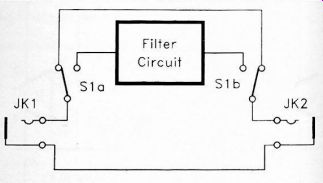
Fig. 2.10 Using a d.p.d. t. to provide bypass switching around a filter
PA Filtering
If you need highpass or lowpass filters having different cut-off frequencies to the scratch and rumble filter circuits, it will probably not be difficult to alter these circuits to suit your requirements. You might require a minor change in frequency simply because you would prefer (say) a scratch filter with a somewhat lower cut-off frequency to combat more severe scratches. On the other hand, you might require a large change in order to suit a totally different application.
Both are easily accommodated.
The cut-off frequency of the scratch filter can be altered by changing the values of the filter resistors and (or) capacitors.
In practice it is generally easier to change the value of the three resistors. The cut-off frequency is inversely proportional to the value of these resistors. In other words, doubling their value halves the cut-off frequency - halving their value doubles the cut-off frequency. A little mental arithmetic should produce a suitable value for an alternative cut-off frequency. It may be possible to "tweak" one or more of the filter capacitor values to suit your requirements, but this is by no means essential.
The cut-off frequency of the rumble filter can also be altered by changing the values of the resistors and (or) capacitors in the filter network. In this case it is generally easier to alter the value of the three capacitors, and then leave the resistor values unchanged, apart from any slight "tweaking" to optimize performance. Again, the cut-off frequency is inversely proportional to the values of the filter components.
Filtering is sometimes used in PA equipment to restrict the audio bandwidth to the frequencies that are most important for speech signals. This helps the speech signal to stand out from what will often be quite a hub-bub of background sounds.
In some cases only topcut filtering is used. When only topcut filtering is used it is mainly included as a means of reducing problems with acoustic feedback and the dreaded "howl around". The optimum cut-off frequencies are about 2.5kHz for the lowpass filter, and about 300Hz for the highpass filter.
A cut-off frequency of 2.5kHz is not quite one-third of the scratch filter's 7kHz cut-off point. Therefore, multiplying the 4k7 filter resistor value by a little under three will give a suitable resistor value. 4k7 multiplied by three equals 14.1k, and the next value down from this in the E12 series of values is 12k, which should give something very close to the required cut-off frequency.
The rumble filter has a cut-off frequency of 100Hz, but we require a figure some three times higher. The filter capacitors therefore need to be one-third of the original value (which was 220n). 220n divided by three equals 73.33n, and the nearest El 2 value to this is 68n.
Figures 2.11
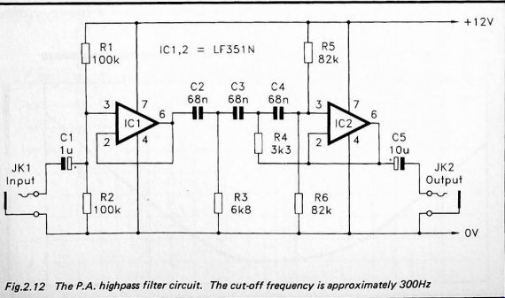
Figures 2.12
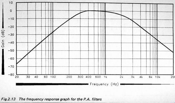
Figures 2.13
Figures 2.11 and 2.12 are respectively for lowpass and highpass filters for PA applications. These follow the design method described above, and as can be seen from the frequency response graph of Figure 2.13, these changes in value have very much the desired effect.
Components for Figure 2.11
Resistors (all 0.25 watt 5% carbon film)
100k
100k R1 R2 R3 12k R4 12k R5 12k
Capacitors
C1 1u 63V elect 10n polyester 5% or better 15n polyester 5% or better In polyester 5% or better 10u 50V elect C2 C3 C4 C5
Semiconductors
IC1 LF351N
LF351N IC2
Miscellaneous
JK1 standard jack socket standard jack socket
Case, circuit board, two 8 pin d.i.l. i.c. holders, wire, solder, etc.
JK2
Components for Figure 2.12
Resistors (all 0.25 watt 5% carbon film)
100k
100k R1 R2 6k8 R3 3k3 R4 82k R5 R6 82k
Capacitors
C1 1u 63V elect 68n polyester 5% or better 68n polyester 5% or better 68n polyester 5% or better 10u 50V elect C2 C3 C4 C5
Semiconductors
LF351N
LF351N IC1 IC2
Miscellaneous
JK1 standard jack socket standard jack socket
Case, circuit board, two 8 pin d.i.l. i.c. holders, wire, solder, etc.
JK2
Tone Controls
Tone controls seem to be a feature of most audio amplifiers, and these are usually in the form of bass and treble controls capable of providing about 12dB or so of boost or cut over their respective frequency bands. Although they are very simple circuits, many tone control designs seem to have rather unusual control characteristics if you make some careful checks on them! The problem is usually a lack of symmetry in the boost/cut characteristic. This is not really a fatal flaw, but it does mean that the central control settings will not give the expected flat frequency response.
One cause of the problem is that some tone control circuits are passive types, and are therefore dependant on having suitable source and load impedances. Errors in either can cause unwanted changes in the responses of the controls.
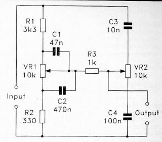
Fig.2.14 The circuit diagram for a simple passive tone control network
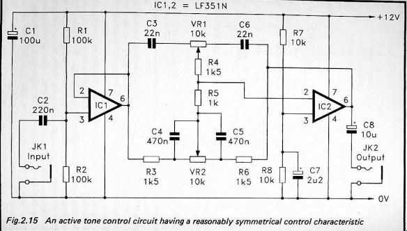
Fig.2.15
Figure 2.14 shows the circuit diagram for a simple passive tone control that will work reasonably well provided it is fed from a low source impedance and feeds into a reasonably high load impedance. Being a passive device it is not really correct to talk in terms of the controls providing boost and cut. The circuit always provides losses, and when set to provide bass or treble boost it is in fact providing reduced losses rather than a genuine boost to the signal level. This is not purely academic, and the system as a whole must be designed to take into account the basic loss of about 12dB through a circuit of this type.
My advice would be to not bother with passive circuits, and to instead opt for an active tone control circuit such as the one shown in the circuit diagram of Figure 2.15. This is basically just a passive tone control connected in the feedback circuit of a non-inverting amplifier, plus an input buffer stage to ensure that the main tone control circuit is driven from a suitably low source impedance. This gives a sort of inverted action, where boost from the tone controls gives more feedback and reduced gain, and cut from the controls gives less feedback and more gain. However, provided the tracks of the two potentiometers are wired to take this into account, you will get the correct action from them (i.e. clockwise rotation giving boost; counter-clockwise rotation giving cut).
The circuit provides a little in excess of 12dB of boost and cut at the extremes of the audio range. Figure 2.16 shows the approximate frequency responses of the two controls when set for maximum boost and cut. These responses have quite good symmetry, and the circuit gives something very close to a flat response when the controls are set at the middle position.
However, bear in mind that the tolerances of potentiometers are quite wide at about 20%, and that the mechanical mid-point is unlikely to be the true electrical mid-point. Any errors this produces in the supposedly flat frequency response should be quite minor though.
Construction of the tone controls presents no major difficulties. The voltage gain is so low, even when set for maximum boost, that there is no great risk of instability.
Remember to get the tracks of the controls wired round the right way. Treble control VR1 provides boost with the wiper set towards the C3 end of the track, or cut with it set towards the C6 end. Similarly, bass control VR2 provides boost with the wiper set towards the R3 end of the track, or cut with it at the R6 end of the track. Note that there is a small voltage gain of about four or five times through the circuit at the 0dB reference level.
Components for Figure 2.14
Resistors (all 0.25 watt 5% carbon film) R1 3k3 R2 330R R3 1k
Potentiometers VR1 VR2 10k lin carbon 10k lin carbon
Capacitors
47n polyester 5% or better
470n polyester 5% or better
C1 C2
2.15
2.16
C3
10n polyester 5% or better
100n polyester 5% or better
C4
Miscellaneous
Two control knobs, wire, solder, etc.
Components for Figure 2.15
Resistors (all 0.25 watt 5% carbon film)
100k
100k R1 R2 lk5 R3 lk5 R4 R5 1k R6 lk5 10k R7 10k R8
Potentiometers
VR1 VR2 10k lin carbon 10k lin carbon
Capacitors
100p 25V elect 220n polyester 22n polyester 5% or better 470n polyester 5% or better 470n polyester 5% or better 22n polyester 5% or better 2u2 63V elect 10m 50V elect C1 C2 C3 C4 C5 C6 C7 C8
Semiconductors
LF351N
LF351N IC1 IC2
Miscellaneous standard jack socket JK1
JK2 standard jack socket
Two 8 pin d.i.l. i.c. holders, circuit board, wire, solder, etc.
Loudness Filter
I always think that the name "loudness" filter is a rather inappropriate one for this type of filter. It is actually one that is for use when operating an audio system at low volume levels. It would therefore seem more apt to call it a "quietness" filter. Anyway, the idea of such a filter is that it should compensate for the seeming reduction in high and low frequency signals when listening at low volume levels. This is apparently due to the way the human hearing system operates, and the way in which the brain decodes the signals from the ears. The degree of boost needed is quite low, and most loudness filters provide only about 6dB or so of boost at bass frequencies, and somewhat less than this at high frequencies.
A pair of ordinary bass and treble tone controls can actually provide suitable filtering, but a separate loudness filter provides a more convenient means of achieving much the same thing.
The circuit diagram of Figure 2.17 is for a simple loudness filter which provides about 6dB of boost at bass frequencies, and around 3dB to 4dB of boost at treble frequencies. Figure 2.18 shows the approximate frequency response of the circuit.
The circuit is basically just a non-inverting amplifier with two types of frequency dependant negative feedback.
The bass boost is provided by C5 and R6. At most frequencies the impedance of C5 is low in comparison to that of R6, and R6 is therefore shunted across R5. At low frequencies the impedance of C5 becomes significant, and reduces the shunting effect of R6. This gives a higher feedback resistance, and somewhat boosted gain. The boost in gain is tamed by the inclusion of R5, which sets a suitable upper limit on the feedback impedance.
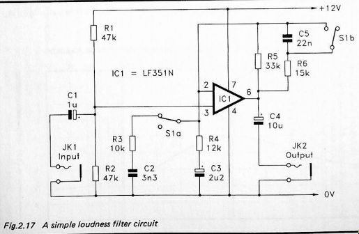
Figure 2.17
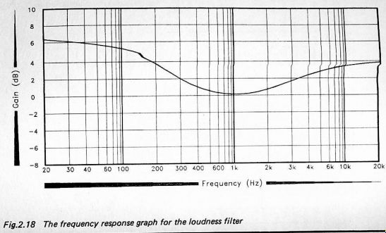
Figure 2.18
In the other section of the feedback network, R4 is shunted by R3, but only at high frequencies where C2 has a low impedance. This gives the high frequency boost, and R3 tames the response so that the required modest boost in gain is produced. SI enables the loudness filtering to be switched out without producing any significant change in the voltage gain at middle frequencies. SI a simply switches out R3 and C2 so that the high frequency boost is eliminated. Sib short circuits C5 so that R6 shunts R5 at all frequencies.
Once again, construction of this project should offer no real problems. The component layout is not critical. Although the circuit shows the unit as having input and output sockets, obviously it does not have to be built as a stand-alone unit.
If it is built into an amplifier the input and output sockets are unnecessary. The same is true of most of the circuits featured in this guide.
Components for Figure 2.17
Resistors (all 0.25 watt 5% carbon film)
47k R1 R2 47k R3 10k R4 12k R5 33k R6 15k
Capacitors
63V elect 3n3 polyester 2u2 63V elect 10 u 50V elect 22n polyester
C1 C2 C3 C4 C5
Semiconductor
LF351N IC1 Miscellaneous standard jack socket standard jack socket d.p.d.t. toggle 8 pin d.i.l. i.c. holder, circuit board, case, wire, solder, etc.
JK1 JK2 S1
Mixers
Mostly it is only necessary to feed a power amplifier from one signal source at a time. A rotary or push-button switch assembly is used to select the required input socket, or the output from the appropriate preamplifier, and connect it through to the input of the power amplifier. Some applications require a mixer though. This is usually where the equipment must be fed from two sources simultaneously, such as a tape deck providing background music and a microphone preamplifier for the "live" commentary. Mixer inputs can also be used to give a sort of pseudo automatic input selection.
Instead of selecting the appropriate signal source, you simply activate the one you require and it will be fed through to the power amplifier by the mixer stage.
Figure 2.19 shows the circuit diagram for a simple four input mixer. This is basically just an ordinary inverting amplifier circuit, but it has an input socket, input resistor, and d.c. blocking capacitor for each of four inputs. This is called a "summing mixer" circuit. The circuit operates much like a basic inverting mode amplifier, but the output must balance the sum of the input signals. It is from this summing action that this circuit configuration gets its name. This is actually the sort of circuit operational amplifiers were originally designed for, but using d.c. signals instead of a.c. types.
There is unity voltage gain from each input to the output, but the voltage gain could obviously be increased by making R7 higher in value. The voltage gain is set by feedback resistor values in normal inverting amplifier fashion. The input impedance is, of course, 100k at all four inputs.
Although the circuit is shown as having four inputs, in theory it is possible to have any desired number of inputs.
Just add an input socket, coupling capacitor, and input resistor for each input you require. In practice there are limits on the number of inputs that can be used. There is no strict upper limit though - it depends on how much noise and distortion you are prepared to tolerate.
The first point to note is that each extra input reduces the performance of the circuit. Having (say) ten 100k input resistors is much the same as having one 10k input resistor.
In other words, with ten inputs and unity voltage gain, the ...
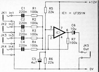
Fig.2.19 A basic
four input summing mode mixer
... operational amplifier has noise and distortion levels that are much the same as a circuit which has one input and a voltage gain of ten times. With the voltage gain at unity, you can obviously have quite a large number of inputs without the performance of the circuit dropping to an inadequate level.
However, if you opt for a certain amount of voltage gain through the circuit, using a lot of inputs might not be acceptable. For instance, ten inputs plus a voltage gain of ten times gives the operational amplifier an effective voltage gain of 100 times. This is unlikely to give acceptable results. If you wish to have a large number of inputs, keep the voltage gain low.
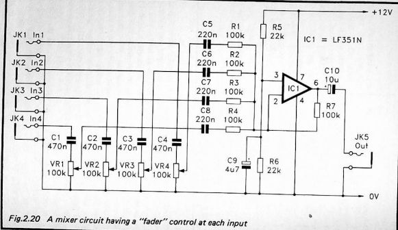
Fig.2.20
In reality it is often not the effective gain of the operational amplifier that governs the maximum number of inputs that can be used. Having a large number of inputs tends to produce a lot of wiring at the input of the circuit, which in turn results in significant pick-up of mains "hum", etc. If you are going to have a large number of inputs it is essential to keep all the input wiring as thoroughly screened as possible.
If a mixer having an input level control for each input is required, it is basically just a matter of adding a "fader" potentiometer at each input. The circuit diagram for a mixer of this type is shown in Figure 2.20. Again, this is shown as a four-input mixer, but by adding extra sets of input components it is possible to have more inputs. Note though, that this type of mixer has much more wiring per input, and is therefore more vulnerable to stray pick-up in the input wiring.
Adding the "faders" reduces the input impedance at each input from 100k to around 50k.
Construction of the mixer units should be fairly straightforward. However, as already pointed out, if you are using a large number of inputs the component and general layout needs to be carefully thought out so that there is minimal input wiring.
Components for Figure 2.19 Resistors (all 0.25 watt 5% carbon film)
100k
100k R1 R2 100k R3 100k R4 22k R5 22k R6 100k R7
Capacitors 220n polyester 220n polyester 220n polyester 220n polyester 4^7 63V elect 10u 50V elect
C1 C2 C3 C4 C5 C6
Semiconductor
LF351N IC1
Miscellaneous standard jack socket standard jack socket standard jack socket standard jack socket standard jack socket 8 pin d.i.l. i.c. holder, circuit board, wire, solder, etc.
JK1 JK2 JK3 JK4 JK5
Components for Figure 2.20
Resistors (all 0.25 watt 5% carbon film)
100k
100k R1 R2 100k R3 100k R4 22k R5 R6 22k 100k R7
Potentiometers
VR1 VR2 VR3 VR4 100k log carbon 100k log carbon 100k log carbon 100k log carbon
Capacitors
470n polyester
470n polyester
470n polyester
470n polyester
220n polyester
220n polyester
220n polyester 220n polyester 4pl 63V elect 10p 50V elect
C1 C2 C3 C4 C5 C6 C7 C8 C9 C10
Semiconductor
LF351N IC1
Miscellaneous
JK1 standard jack socket standard jack socket standard jack socket standard jack socket standard jack socket
Four control knobs, 8 pin d.i.l. i.c. holder, circuit board, wire, solder, etc.
JK2 JK3 JK4 JK5
----- Fig.2.21
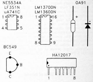
Semiconductor pinout details (I.C.s are top views, transistor is base view)
NE5534A LF351N uA74IC
LM13700N LM13600N
BC549 HA12017
---------
Index | Prev.