The R-C coupled AF voltage amplifier circuit is one of the simplest amplifier circuits available. It is widely used for amplification of signals in the audio range, up to 10,000 or 20,000 cycles per second. The circuit goes by the name of RC amplifier, which refers to the combination of resistive load and coupling capacitor.
It also is frequently referred to as a resistance-coupled amplifier.
CIRCUIT DESCRIPTION
When a signal voltage of a given amplitude (strength) 1s impressed on the control grid (input circuit), a signal voltage of larger amplitude will be delivered in the plate circuit, or output circuit. The accompanying diagrams portray the essential circuit actions occurring in two successive half-cycles. Fig. 1 depicts current ( electron) flow conditions during an entire half-cycle of the signal which will be referred to here as a negative half-cycle; and also the instantaneous-voltage conditions at the midpoint of that same half-cycle.
Fig. 2 depicts the same current flow for the entire second half cycle, and the voltage conditions at the midpoint of the second half-cycle. This, we will call the positive half-cycle.
The circuit components for the resistance-coupled AF voltage amplifier are:
R1-Grid load resistor for V1.
R2-Cathode biasing resistor.
R3-Plate load resistor.
R4-Grid load resistor for following stage.
C1-Cathode bypass capacitor.
C2-Coupling capacitor to following stage.
V1--Triode amplifier tube.
M1--Power supply.
There are three main currents at work in the circuit. Each has been shown in a separate color in Figs. 1 and 2. They are:
1. Grid-driving current for stage (blue) .
2. Plate current of the tube (red).
3. Grid-driving current for following stage (green).
The first current, flows in the input circuit and is called the grid-driving current (blue) . It is directly associated with the grid-driving voltage ( also shown in blue) , a more common term than grid-driving current in discussing tube operation.

Fig. 1. The R-C coupled audio amplifier-negative half-cycle.
The second current is the unidirectional tube current, shown in red and called the plate current. The current which flows into and out of output coupling capacitor C2 and the cathode filtering current are also shown in red because of their dependence on the unidirectional tube current.
The final current, which is actually flowing in the next tube circuit and is not intrinsically a part of the RC amplifier, is the grid-driving current for the next tube stage. It is shown here (in green) to make easier the comparison between input and output voltages and thereby further clarify the term amplification.
Undoubtedly the most important single characteristic of vacuum tubes having control grids is their ability to amplify voltages. The valving, or throttling, action of the control grid within the tube makes it possible for small voltage changes impressed on the control grid to cause fairly large changes in the amount of electron current flowing through the tube. These large changes in tube current can then be made to generate larger voltage changes in the plate circuit. The output voltage should faithfully reproduce the waveshape of the input voltage, with no distortion. however, this goal is not always attained. The degree to which this is achieved determines the fidelity of the circuit.

Fig. 2. The R-C coupled audio amplifier-positive half-cycle.
CURRENT FLOWS
In Fig. 1, a small electron current is shown, in blue, flowing downward through the grid resistor R1. The control grid will be at its maximum negative voltage when maximum current is flowing downward through the grid resistor. Since Fig. 1 represents an entire half-cycle, the moment of maximum negative grid voltage occurs roughly near the midpoint of this half-cycle. The unidirectional tube current, shown in red, will be throttled down to its minimum value by this negative grid voltage.
The second diagram shows this grid-driving current flowing upward through resistor R1, in response to the positive voltage impressed from the external circuit. The maximum flow rate, and the resultant maximum positive voltage at the grid, will occur roughly at the midpoint of the second half-cycle. The unidirectional tube current will then flow at its maximum value.
If no signal voltage were applied to the grid, the tube current (plate current) would flow in a steady stream through the path indicated-that is, up from ground through cathode resistor R2, through the tube, downward through plate-load resistor R3 and the power supply to ground, then back to the cathode resistor.
This is the quiescent, or static, operation of the tube. When a small signal voltage imposes fluctuations on the electron stream through the tube, these fluctuations develop larger voltage variations in the plate circuit, and the input signal is considered to be amplified.
This amplified signal voltage can perhaps best be explained by referring to Fig. 2. The increase in plate current ( due to the positive grid voltage) is causing electrons to be dammed up at the entrance to plate-load resistor R3. These electrons are shown pouring onto the left-hand plate of the coupling capacitor C2, thereby reducing the positive voltage stored on that plate. At the same time, on the other side of this coupling capacitor, electrons are being driven away from the capacitor and downward through R4, the grid resistor for the next tube stage. (This is the current shown in green). Thus, we can see that a phase shift has occurred in this amplifier stage, for when the first grid is at maximum positive voltage, the second grid is at its maximum negative voltage.
The voltage on the left side of coupling capacitor C2 does not actually become negative, but varies between low and high values of positive voltage. To indicate this, the two red plus signs at this point in Fig. 1 have not been replaced by minus signs, but are merely changed to a single plus sign to signify the reduction in voltage caused by the additional electrons from the plate-current stream.
Simultaneously with this action, more electrons will flow through plate-load resistor R3 toward the power supply, causing an increased voltage drop across this resistor. Since the voltage at the lower end is fixed (being connected directly to the power supply voltage), this increased voltage drop across the load will be evidenced by a decrease in the positive voltage at the top of resistor R3.
Thus we have two means of associating a drop in plate voltage with an increase in plate current. One is by the inflow of electrons into coupling capacitor C2, neutralizing an equal number of positive ions there. The second is by the increased electron flow through load resistor R3.
Fig. 1 depicts the half-cycle when the tube current is restricted by the negative grid voltage. Minimum plate current is indicated during this period. This decrease in current affords an opportunity for the low positive voltage on the left plate of C2 to build up again. Electrons will now be drawn out of this capacitor and toward the power-supply voltage. As they depart, there is an attendant increase in the number of positive ions remaining at this point and the voltage increases to a higher positive value.
This departure of electrons from the left plate of the coupling capacitor draws an equal number of electrons upwards through the grid resistor and onto the right plate (shown in green). Thus, we have two means of visualizing that the voltage changes imparted to the grid of the next tube will duplicate, or follow, the voltage changes in the plate circuit of the amplifier stage.
When electrons flow downward through R4 (green in Fig. 2), we know that the top of R4 is more negative than the bottom, or ground. This action coincides with the period of increased tube current which, as mentioned, has reduced the positive plate voltage.
CATHODE CIRCUIT
In the cathode circuit, capacitor C1 functions as a filter to pre vent degeneration. The resulting filtering current is being driven by the fluctuations in demand for electrons at the cathode. In the Fig. 1, the control grid is negative, so the demand for electrons to enter the tube is not great. However, since the upper plate of the capacitor is already charged to a positive voltage, this voltage will draw electrons upward through cathode resistor R2. During the first half-cycle they are shown flowing onto the upper plate of the capacitor and of course neutralizing some of the positive ions there which make up the positive voltage on the cathode.
During the second half-cycle (Fig. 2) when the control grid is positive, the demand for electrons in the plate current stream is greatly increased. This bigger demand is supplied by free electrons from the upper plate of the capacitor. The departure of these electrons naturally creates additional positive ions on the capacitor plate.
These changes in the quantity of positive ions naturally would indicate a change in the positive voltage at the cathode. However, normal amplifier operation requires an unchanging cathode voltage. The answer to this apparent paradox lies in the amount of voltage change which occurs because of this regular inflow and outflow of electrons. To determine the amount of voltage change, a factor known as the time constant must be considered.
Time Constant
The time constant of a circuit is the time required by a resistance-capacitance combination to complete 63.2% of its charging or discharging action. Numerically, the time constant is equal to:
T=RXC
where,
T is the time in seconds,
R is the resistance in ohms,
C is the capacitance in farads.
Any RC combination is defined as a "long time-constant" circuit when the value of T is "long" (five or ten times as long), compared with the time which elapses during one cycle of the frequency under consideration, and as a "short-time constant" circuit if significantly (five or ten times) shorter than the frequency under consideration.
Thus, if we make the time constant of the resistor-capacitor combination in the cathode circuit (C1 and R2 in Figs. 1 and 2-2) long, it will provide a relatively constant voltage at the cathode. If the signal frequency is 1,000 cycles per second, then the time required for one cycle is .001 second. Thus the time constant of this combination should be at least .005 seconds. Any combination of resistor and capacitor values whose product exceeds .005 second would theoretically meet this requirement. However, one additional consideration, which virtually dictates the size of the resistor, is the amount of positive voltage wanted at the cathode (cathode biasing voltage). Since all the tube current is going to pass through the cathode resistor, we can calculate by Ohm's law what size of resistor we would need, with a given optimum tube current, to achieve the desired cathode bias voltage.
Ohm's Law
Ohm's law states that the voltage developed across a resistor is proportional to the current through it, or:
E=IxR
where,
E is the voltage developed, in volts,
I is the current in amperes,
R is the resistance in ohms.
Any capacitor plate which is charged to a negative voltage can be looked upon as an electron pool, since electrons in concentration constitute a negative voltage. Likewise, when charged to a positive voltage (as is the upper plate of C1 in this example), a capacitor plate can be considered an ion pool.
The amount of voltage in any such charge is directly proportional to the quantity of electrons or ions which are so concentrated. This is expressed by Coulomb's law, which states that:
Q=CXE
...where, Q is the quantity of charge in coulombs, C is the capacitor size in farads, Eis the voltage.
One coulomb equals slightly more than half a trillion, trillion electrons (6.25 X 10^18, to be exact!). A coulomb of positive charge equals the same number of positive ions.
Filter Action
As indicated before, the actual number of electrons entering the tube is determined primarily by the construction of the tube, as is the size of the variations in this electron stream which are imposed by the alternating signal voltage. The size of the tube current variations determines the quantity of electrons which actually flow onto the upper plate of capacitor C1 during the first half-cycle and off it during the second. If the quantity of positive ions already stored there (which represent the positive cathode voltage) i:; substantially greater than the number of electrons which flow in during the first half-cycle, the positive cathode voltage will not be appreciably affected. But if the electrons flowing in and out of the capacitor during each cycle is a significant fraction of the total number of ions stored there, the ion level will rise and fall, and the positive cathode voltage, being dependent on the ion level, will rise and fall too.
As an example, suppose the desired cathode voltage is + 10 volts and the number of electrons flowing in during the first half cycle is exactly 1 % of the number of positive ions stored there.
Then the cathode voltage would be reduced by 1%, or 0.1 volt, thereby making its value 9.9 volts on this half-cycle. On the second half-cycle, with the same number of electrons leaving the capacitor, the stored voltage would again increase to the full 10 volts.

Fig. 3. Grid and plate waveforms for an R-C coupled audio amplifier.
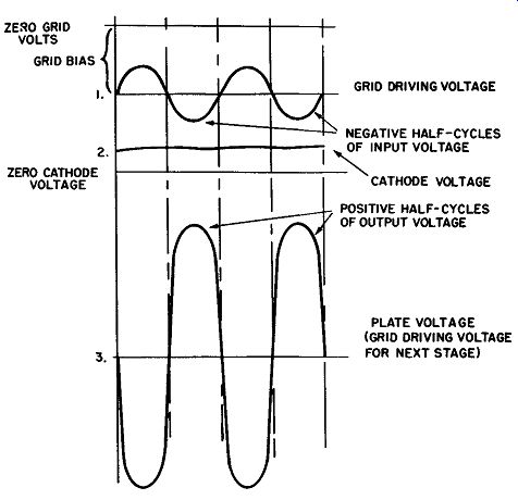
Fig. 4. Relationship between grid, cathode, and plate voltages in an R-C
coupled audio amplifier.
Filtering is completed by allowing current to flow between the lower plate of the filtering capacitor and ground. This current, shown in red, is driven downward during the first half-cycle by the inflow of electrons to the top plate, and upward during the second half-cycle by the outflow of electrons going toward the cathode. The electrons flowing along this path will always equal in quantity the electrons flowing to or from the other side of the capacitor. If this current were restricted somehow from flowing, filtering could not be done.
The variation in cathode voltage, as a result of the changes in tube current, is a measure of the degeneration which occurs. In other words, degeneration reduces the total amplification the tube can deliver.
WAVEFORM ANALYSIS
Fig. 3 is the conventional waveform diagram for relating the grid-driving voltage, the biasing or reference voltage, and the plate current. This relationship is achieved by means of the transfer characteristic curve of the tube.
For any instantaneous grid voltage, a line projected vertically to the transfer characteristic curve and thence horizontally to the plate-current scale will indicate in milliamperes the resulting plate-current flow.
The plate-voltage sine wave is given below the one for the plate-current. Of special interest is the fact that when plate current is maximum, plate voltage is minimum, and vice versa. This illustrates the phase shift which occurs between grid and plate voltages in most vacuum tubes. When the grid voltage is most negative, the plate voltage is most positive; when the grid voltage is least negative, the plate voltage is least positive.
Fig. 4 shows this phase relationship between input and output voltages more clearly. The cathode voltage has also been shown in Fig. 4. Notice that it is essentially a flat line, increasing very slightly during those half-cycles when the tube conducts most heavily.
FREQUENCY RESPONSE
Response Curve
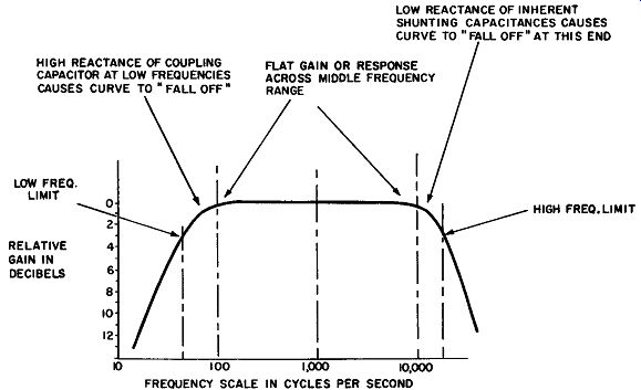
Fig. 5. An R-C coupled audio amplifier response curve.

Fig. 6. Current flow at low, medium, and high frequencies in the R-C coupled
audio amplifier-positive half-cycle.
Fig. 5 shows a conventional frequency-response curve for a resistance-coupled amplifier. Below 100 cycles per second (cps). the response of the amplifier falls off because the signal is attenuated, or "consumed," by coupling capacitor C2. Capacitive reactance varies inversely with the frequency of the applied signal, in accordance with the standard formula: where, 1 X('=- 2 pi fC X1, is the capacitive reactance in ohms, f is the frequency in cycles per second, C is the capacitance in farads.
Thus, at very low frequencies the coupling capacitor will couple, or "pass," only a small portion of the available signal from the plate circuit of the tube to the grid circuit of the next tube, and will attenuate most of the signal as it passes through.
The response of an amplifier circuit is a measure of how well it amplifies a voltage at any particular frequency. The response curve is a means of comparing how well it responds to, or amplifies, voltages at any frequency within the range of the amplifier.
The curve will also indicate the frequency limits within which the amplifier is designed to operate. It is very important in design consideration that an amplifier response curve be flat and that the sides be as steep as possible. A flat response curve indicates that the circuit will provide equal amplification for applied voltages of any frequency within its range. An amplifier which did otherwise would provide very poor sound reproduction indeed.
The high-frequency limit of operation for a resistance-coupled amplifier is determined by the interelectrode capacitances of both tubes and by the distributed or wiring capacitances of the entire circuit. Fig. 6 shows the equivalent circuit of the RC amplifier in Figs. 1 and 2. The cathode, grid, and plate of the next succeeding triode stage have been added in Fig. 6 because they have a definite bearing on the high-frequency limit of operation.
Three different currents are shown passing simultaneously through the amplifier tube:
1. Low-frequency current, (green)
2. Medium-frequency current, (red)
3. High-frequency current, (blue)
Let us define these terms. The low-frequency current is one having a frequency lower than the low-frequency limit of the response curve in Fig. 5, and the high-frequency current is one having a frequency higher than the high-frequency limit. Each of these limiting points is defined as being the point at which the amplifier response has fallen 3 decibels from the response achieved across the flat area of the curve.
It should be assumed that equal amplitudes or amounts of each of these three frequency components are applied at the input point, meaning the control grid of the first tube, V1. These three components of current are all shown as flowing upward through grid driving resistor R1 in Fig. 6. Since the frequencies of these three currents are drastically different, the time durations, or "periods," for single cycles at the three frequencies will differ greatly from each other. Consequently, the actual condition depicted in Fig. 6, where the three currents appear to be flowing in phase with each other through the grid resistor, would be achieved only rarely. There is an infinite variety of combinations when three such currents of three widely separated and variable frequencies can be somewhat out of phase with each other. But there is only one combination when they can all reach their maximum amplitude, in the same flow direction, at the same instant, thereby being truly in phase with each other as depicted in Fig. 6.
As an example, consider the following possible frequencies and resulting periods for one cycle of each of the three currents. The period of a sine wave is related to the frequency by the formula: where,
T is the time for one cycle in seconds, F is the frequency in cycles per second.
Current
Low Frequency Middle Frequency High Frequency
Frequency, F
50cps 1,000 cps 20,000 cps
Time for One Cycle, T
.02 sec.
.001 sec.
.00005 sec.
In addition to the normal "manufactured" circuit components in Fig. 6, there are inherent characteristics which place the upper limit on the frequency response of a resistance-coupled amplifier like this one. These inherent characteristics include:
1. The output capacitance of amplifier tube V1. This is shown in dashed lines between the plate of V1 and its cathode, and is labeled C0
2. The distributed capacitance between all the w1rmg of the circuit and the nearest ground points. This is normally shown in equivalent circuits as a single, or "lumped," capacitance and is labeled Cd.
3. The input capacitance of the next amplifier stage. This consists of the inherent interelectrode capacitance between the control grid, and the cathode and plate of the next amplifier stage (designated C1 in Fig. 6). Let us consider now what effects these inherent capacitances may have on the passage of currents at the three chosen frequencies-low, intermediate, and high.
Low-Frequency Limitation
The primary limitation on the passage of low-frequency currents is the reactance of the main coupling capacitor, labeled C,. in Fig. 6. Because of the excessive reactance which all capacitors exhibit at low frequencies, only a very small portion of the avail able low-frequency current can enter this capacitor. An equally small portion of current, at the same low frequency, will be driven out of the opposite plate and be available to flow downward through the grid-driving resistor for the next stage labeled as R4 in Fig. 6). The amount of grid-driving voltage developed at any frequency depends on the amount of current, at this same frequency, which can be made to flow through the grid-driving resistor. In Fig. 6 the low-frequency current flowing in the circuit to the right of capacitor Cc is in dashed green lines to indicate the severe attenuation it suffered in getting through the coupling capacitor.
The classical method of verifying the extent of this attenuation is to calculate the reactance of the capacitor at the particular frequency, and to compare it with the resistance of the grid driving resistor, since these two components comprise the complete path of this current. At the low frequency of fifty cycles per second, the reactance of capacitor C,. will be twenty times as great as it is at 1,000 cps, and two hundred times as great as it is at 10,000 cps. (Reactance, of course, is the measure of a capacitor's opposition to electron flow.) At 50 cps the coupling reactance so greatly exceeds the grid resistance that most of the low-frequency signal is lost in the capacitor.
Middle-Frequency Current Passage
The middle-frequency current, shown in red in Fig. 6, can have any frequency in the entire middle range between the low and high-frequency limitations shown in Fig. 5. In passing through the coupling capacitor, the current has only insignificant losses. Most of it is available to flow up and down through R4 ( on alternate half-cycles, of course) and develop grid-driving voltage for tube V2. The inherent capacitances (Cd and Ci) have small values, on the order of 10 micro-microfarads each; consequently, their reactances are prohibitively large throughout the entire range of low and middle frequencies, and little or none of the signal currents bleed off at these frequencies.
High-Frequency Limitations
The range of higher audio frequencies is where the inherent capacitances of vacuum tubes and their circuitry limit the operation of audio-frequency amplifiers. The reason is that excessive quantities of the available current are bled off, leaving little or none to flow through grid resistor R4 and develop driving voltage for the next stage. The high-frequency currents are indicated in blue in Fig. 6. We see that some portion of the high-frequency currents are bypassed back to the cathode of tube V1 by the output capacitance, C_O , of the tube. At the high frequencies this action reduces the amount of signal current available for coupling across C1, to the next stage.
The signals suffer no intrinsic loss at the higher frequencies as they pass through coupling capacitor C,., since the reactance of all capacitors decreases as the frequency increases. It is thus possible to say that there is negligible voltage drop, or only slight attenuation of its voltage, as the signal is passed through the coupling capacitor.
That portion of higher-frequency current which succeeds in getting through coupling capacitor C,., finds four alternate paths available to it, all in parallel. Consequently the current will divide into four parts, the amount going to each part being inversely proportional to the impedance offered by each particular path.
Only the current which manages to flow up and down through grid resistor R4 will develop driving voltage for the next stage; the other three are losses.
The distributed, or wiring, capacitance of the circuit has been represented by the simulated capacitor Cd. In Fig. 6 we see the high-frequency current flowing freely into this simulated capacitor and thus being bypassed to ground. This is the first of the three loss currents referred to in the previous paragraph.
The second loss current flows directly into the interelectrode capacitance between the control grid and cathode of tube V2. In Fig. 6 a component of high-frequency current is shown flowing between the cathode and the ground connection. This component is driven by the current flowing toward the control grid from the coupling capacitor, but contributes nothing to the operation of amplifier V2.

Fig. 7. Equivalent circuit at high frequencies in the R-C coupled audio
amplifier-negative half-cycle.
The third loss current associated with this amplifier stage flows in the inter-electrode capacitance between control grid and plate.
In Fig. 6 a component of this loss current is shown flowing away from the plate, since it is being driven by the electrons flowing toward the grid from the coupling capacitor. This current also contributes nothing to the operation of the amplifier stage.
Fig. 7 shows the equivalent circuit of Fig. 6, but redrawn with only the high-frequency currents flowing, since the inherent capacitances discussed earlier are significant at the higher frequencies only. The flow directions of currents in Fig. 7 are the reverse of those in Fig. 6. Fig. 6 represents conditions during a positive half-cycle of operation, and Fig. 7 represents a negative half-cycle.
Therefore, in Fig. 7 the high-frequency signal current is flowing downward through resistor R1, making the control grid of tube V1 negative. As a result, the plate current through tube V1 is reduced and the plate voltage rises. Some portion of the high plate-voltage peak, which would otherwise have been obtain able, will be lost. The reason is that the shunting effect of output capacitance of the tube permits some instantaneous electron current to be drawn upward from the upper plate of C0 • These additional electrons reduce the positive plate-voltage peak somewhat, and consequently are another loss current when the circuit is operated at high frequencies.
As the plate voltage rises (Fig. 7) and falls (Fig. 6), this loss current flows alternately up and down fairly freely, bypassing some of the high-frequency voltage back to the cathode. From here it has an easy bypass path through cathode filter capacitor C1 to ground.
The rise in plate voltage in Fig. 7 also draws current onto the right plate of coupling capacitor C, .. If there were no shunting capacitances to worry about, all of this current would be drawn up ward through grid resistor R4 and a maximum positive voltage peak for application to the control grid of tube V2 would be developed across R4. In reality, some current will be drawn through each of the inherent capacitances and only a small remainder will flow upward through the grid resistor. This explains why all three loss currents are now flowing toward coupling capacitor C,., instead of away from it as in Fig. 6.
FEEDBACK
Often, the output waveform will be distorted, that is, it will not be an accurate reproduction of the input waveform. Feedback is often employed to compensate for any distortion introduced by the circuit and to extend the frequency response of the amplifier.
Figs. 8 and 9 depict two successive half-cycles in the operation of a two-stage resistance-coupled amplifier which utilizes both negative and positive feedback. The positive feedback is achieved by coupling the plate voltage from the second stage back to the control grid of the first stage. The negative feedback is achieved through the degeneration process, by leaving the cathode resistor for the tube unfiltered, or unbypassed. Let us examine these two important actions in more detail. In order to do so, it will prove desirable to review the actions occurring in the entire circuit.
The essential components of this two-stage amplifier are:
R1-Grid input resistor for V1.
R2-Grid input and feedback resistor.
R3-Voltage-divider resistor used in feedback path.
R4-Cathode resistor used for developing negative feedback.
R5-Plate-load resistor for tube V1.
RS-Grid driving, or input, resistor for V2.
R7-Cathode biasing resistor for V2.
R8-Plate-load resistor for V2.
R9-Grid-driving, or input, resistor for next stage.
C1-Coupling capacitor between stages.
C2-Cathode filter capacitor for V2.
C3-Feedback capacitor.
C4-Output coupling capacitor to next stage.
V1 and V2-Triode amplifier tubes.
M1--Common power supply for both tubes.
There are seven electron currents operating in this circuit:
1. Three grid driving currents (green).
2. Two plate currents (solid red).
3. One positive feedback current (blue) .
4. One cathode filter current (dotted red).
Analysis of Operation
By inspection of Fig. 8 we see that at the end of the first half-cycle, the control grid of V1 is positive, the control grid of V2 is negative, and the control grid of the next succeeding amplifier stage is positive. These voltage polarities reflect the normal 180° phase shift between the control-grid and plate voltages in an R-C vacuum-tube stage. Since the control grid of the second tube, V2, reaches its most negative value at the end of the first half-cycle, the plate current through this tube will be reduced to its minimum value and its plate voltage will rise to its maximum positive value. This rise in plate voltage is coupled into the feed back network by drawing electrons off the right plate of feed back capacitor C3. As these electrons flow out of the capacitor, toward the power supply, they draw an equal number upward from ground and through voltage divider R2-R3.
This upward flow of electrons makes the voltage at the bottom of resistor R1 positive with respect to ground; this instantaneous feedback polarity is indicated by a blue plus sign. The instantaneous grid voltage for the first tube, V1, is also positive as a result of the grid driving current. Consequently, the sum of these two positive voltages will be a higher voltage at the grid than the input-signal voltage can provide by itself. Because these two voltages are in phase, the feedback voltage (in blue) reinforces the signal voltage (in green) and the feedback is said to be positive.

Fig. 8. An R-C coupled audio amplifier utilizing both positive and negative
feedback-positive half-cycle.

Fig. 9. An R-C coupled audio amplifier utilizing both positive and negative
feedback-negative half-cycle.
This type of feedback is called voltage feedback, since it is in parallel with the plate voltage and in effect is driven by changes in the latter.
During the second half-cycle (Fig. 9), the control grid of V2 becomes positive, releasing a large amount of plate current through that tube and thus lowering its plate voltage. This reduction in plate voltage is coupled into the feedback network. It is convenient to visualize this action as consisting of the excess plate current electrons pouring onto the right plate of capacitor C3, until they can be drawn through load resistor R8 to the power supply. As the electrons enter C3 they drive an equal number off the left plate of the capacitor, and downward through voltage divider network (R3-R2) to ground. This downward flow of electrons tells us the resulting voltage at the top of resistor R2 must be negative with respect to ground, since electrons will always flow away from a negative voltage, to a less negative or a more positive voltage. This instantaneous feedback-voltage polarity has been indicated by a blue minus sign.
The alternating grid voltage for V1 is also negative at this instant, as a result of the downward flow of grid driving current through resistors R1 and R2. Since these two voltages are now both negative, their sum is a higher negative voltage at the grid than the driving signal can achieve alone. Looking at the results from both half-cycles, we see that the feedback voltage reinforces the signal voltage during the whole cycle. This logically gives rise to its designation as positive feedback.
Current Feedback
During the first half-cycle in Fig. 8, the positive grid voltage on V1 releases a large amount of plate current through this tube.
This plate current flowing upward through resistor R4 to the cathode produces positive voltage (indicated by the plus signs)
at the cathode.
When the control grid V1 is negative (Fig. 9) the plate current through the tube decreases. This causes a smaller voltage drop to be produced across the cathode resistor, and thereby lowers the positive voltage at the cathode. The result of these two actions is a continual fluctuation in the cathode voltage-rising when the grid voltage goes positive, and falling when it goes negative.
An increase in the positive voltage at a cathode has the same effect as a decrease in grid voltage-namely, the amount of plate current flowing across the tube is restricted. The reason for this behavior is that the cathode "recaptures" some of its own electrons after initial emission occurs. This recapturing process comes about in the following manner: When an electron is first emitted into the tube, it "sees" or "feels" (is subject to) whatever voltage exists on any electrode. The high positive plate voltage will try to attract the electron across the tube. A positive voltage at the grid, indicated in Fig. 8, will encourage this process, by allowing a large number of electrons to flow from cathode to plate, resulting in a heavy plate current. However, as the cathode voltage becomes more positive, it will tend to re-attract the emitted electrons after emission. The cathode has two advantages over the other electrodes-(1) the instant after emission, the electron is closer to the cathode than to any of the other electrodes, and (2)
the electron has not yet had the opportunity to build up any velocity as it travels away from the cathode. Consequently, even a slight increase in positive voltage at the cathode causes many of the emitted electrons to fall back onto the cathode, making fewer electrons available for plate current.
In the example of Fig. 8, the increase in the cathode voltage nullifies part of the effect of the positive voltage applied to the control grid by the input signal. Recall that the definition of instantaneous grid bias is the instantaneous difference in voltage between the grid and cathode of a tube. It is this difference between the two voltages that determines what portion of the emitted electrons will be permitted to cross the tube and become plate current.
In Fig. 9 we find an opposite set of conditions. The negative voltage at the grid of a tube will tend to repel most of the emitted electrons back to the cathode. However, since the positive cathode voltage has now been reduced, the cathode exerts less attraction for these electrons and so partially counteracts the negative grid voltage.
This is classified as a form of negative feedback since these continuing changes in the voltages at grid and cathode are "out of phase" with each other. Here the term "out of phase" refers to the effects of changing each of the two voltages, rather than to changing their polarities. Viewed in this light, a rise in the positive grid voltage is out of phase with a rise in the positive cathode voltage.
This type of negative feedback has the more familiar title of degeneration. The obvious result of degeneration is some loss in the amplifying capability of the circuit. Degeneration is usually avoided by the addition of a filter capacitor of suitable size across the cathode resistor, to make a long time-constant combination.
This is why capacitor C2 and resistor R7 are in this circuit.
This type of feedback is also classified as current feedback, because the feedback voltage is developed directly by the plate current stream flowing through the cathode resistor. It is an interesting anomaly, and one which may provide some confusion, that a separate "feedback current" does not exist as such. In the voltage-feedback example discussed previously, a feedback current has to flow through the voltage-divider network (R2-R3) in order for the necessary feedback voltage to be developed. Often, voltage feedback is used for the negative feedback circuit, too.
Such a feedback circuit is discussed in the next Section in conjunction with the transformer-coupled AF amplifier and ·could be used equally well in an R-C coupled circuit.
There is nothing unique about the remaining operations in the circuit. Each of the grid driving currents (shown' in green) develops a larger, or more amplified, version of the signal voltage than the one at the preceding stage. That is, the alternating voltage across resistor R9 is greater than the voltage across R6, and the latter in turn is greater than the voltage developed across R1 and R2.
AMPLITUDE DISTORTION
Fig. 10 is the transfer characteristic curve of a typical triode tube. Note that it is similar to the curve of Fig. 3. Two cycles of input (grid) voltage are shown, along with the resulting two cycles of output (plate) current. Cycle A, which is similar to the grid driving cycle of Fig. 3, causes the tube to operate along the linear portion of the curve. Being a fairly faithful reproduction of the input waveshape, the resulting plate current is considered to be distortionless.
Cycle B is large enough to make the tube operate at both ends of the transfer characteristic curve. Because the curve is nonlinear at both ends, each half-cycle of Cycle B is badly distorted. Likewise, if either half-cycle of grid voltage drives the tube into one of the nonlinear portions of the curve, the resulting distortion would occur on that half-cycle only, but would still be unacceptable. This could happen if the grid-bias voltage were too small for Cycle A. Then, the grid-bias line would shift to the right, and the positive half cycles of plate current would be distorted. Alternatively, the negative half-cycles would be distorted if the grid-bias voltage were too large (shifting the grid-bias voltage line to the left).
Fig. 10. How amplitude distortion is introduced when tube is operated on nonlinear portion of transfer characteristic curve.
PHASE DISTORTION
Fig. 11 shows two voltage sine waves of different frequencies, both before and after passing through an amplifier (such as the resistance-capacitance amplifier of Fig. 9). The purpose in showing these sine waves is to demonstrate the meaning of phase distortion.
Recall that for each stage of amplification, the signal should be inverted; that is, the output waveform should be 180° out-of-phase with the input. Therefore, in the two-stage amplifier of Fig. 9, the signal should be inverted twice or shifted 360°-a complete cycle. Hence, the output voltage waveform should be exactly in phase with the input waveform. Often, in passing through an amplifier, some frequencies will not be shifted exactly 180° in phase.

Fig. 11. The effect of phase distortion on a waveform.
Phase distortion occurs in an amplifier when currents or voltages of some frequencies suffer only a negligible variation from the normal phase inversion, whereas currents or voltages of other frequencies suffer a somewhat greater shift in phase.
In lines 1 and 3 of Fig. 11, the high-frequency voltage "in" has the same phase as the high-frequency voltage "out." This means the two voltages achieve their peak values, pass through zero, etc., at the same moment. These conditions tell us that no phase shift has occurred in this particular voltage during amplification.
However, lines 2 and 4 show that the low-frequency voltage "in" is not in phase with the low-frequency voltage "out"; the latter has been shifted 90°, or a quarter of a cycle, in phase. This means the output voltage achieves its peak value a quarter of a cycle later than the input voltage.
Phase distortion normally is not a serious problem in the re production of sound because the ear cannot detect it. A moment's reflection will clarify why this is so. When we listen to a sustained chord of music we are listening to several tones of different pitches, each of a different frequency. Assume the low-frequency sound represented by the voltage waveforms of lines 2 and 4 is middle C, which has a frequency of 256 cycles per second. A 90° shift in phase means we will now hear each peak about a thousandth of a second later. Obviously, much greater phase differences, amounting to many whole cycles, can be created by the artist without noticeably degrading the over-all result.
Phase distortion is a more serious problem in the amplification of complex waveshapes. These usually represent the algebraic sum of many simple shapes, such as sine waves of many frequencies. If some (but not all) of these subordinate waveshapes have undergone shifts in phase, the resultant waveshape in the output is likely to look entirely different from the input waveshape.