
by W. Marshall Leach, Jr. [Associate Prof., Georgia Institute of Technology, School of Electrical Engineering, Atlanta, Georgia 30332, USA.]
Introduction
Everyone who enjoys building audio gear has probably given thought to constructing a high-power amplifier which will drive even the most inefficient loudspeakers to super loud levels. When it comes to power, most people agree that the higher the power reserve in an amplifier, the better the sound. There is a simple and logical reason for this. Audio signals can have very high peak power levels that run 10 to 20 times the average power level. Thus the peak power output capability of the amplifier becomes an important consideration if it is not to clip on peaks. As an example, let us consider an amplifier rated at 100 watts average power. (This is erroneously called "watts rms." The abbreviation "rms" stands for "root mean square" and is correctly used only in the specification of the amplitude of a.c. voltages or currents, e.g. volts rms or amperes rms, but not watts rms.) Because the power rating is measured with a sine-wave signal which has a peak-to-average power' ratio of only 2, it follows that the peak power capability of our 100-watt amplifier is 200 watts.
With audio signals having a peak-to-average power ratio of 10 to 20, the amplifier could be operated at an average power level of 10 to 20 watts if it is not to clip on peaks. With a typical loudspeaker efficiency of 0.5 percent, only 50 to 100 milliwatts of undistorted acoustic power could be obtained.
This corresponds to a sound pressure level in the reverberant field of a normal listening room of 99 to 102 dB. Should this be insufficient or if the amplifier is to be used in large rooms or outdoors, a higher power rating will be required.
How much power is enough? This is a question which will certainly receive many answers, depending on who is asked.
Someone with efficient loudspeakers who listens to quiet chamber music may say 10 watts. The audiophile with the latest inefficient loudspeakers who likes to demonstrate them at ear-splitting levels with the newest direct-to-disc re cording may say the sky's the limit. However, most people probably consider a power rating of 250 watts per channel to be an adequate rating for a so-called high-power amplifier.
From the standpoint of circuit design, 250 watts represents a power level which is about the maximum that can be achieved without compromises in the design, exorbitant costs, or both. The only method that can be used to increase the power rating of an amplifier is to increase the peak-voltage swing capability of its output signal. This can be done by designing it with a higher voltage power supply, strapping it, or by adding a transformer between the amplifier and the load which steps up the output voltage. To increase the power supply voltage can require circuit design compromises such as the use of a quasi-complementary output stage rather than a fully complementary one. Strapping and a step-up transformer are also design compromises. Both effectively reduce the load impedance seen by the amplifier which can cause overload or excessive triggering of the amplifier protection circuit. Also, the transformer is incompatible with a direct coupled design, and it can cause intolerable phase shifts and distortion at very low frequencies.
Transistors are inherently low-voltage, high-current devices. Therefore, reliable circuit designs require that the voltage across transistors be held to a value that is low enough to permit them to safely deliver the load currents required for the maximum desired output power. This is especially important when reactive loads such as electrostatic loudspeakers or highly inductive crossover networks must be driven. Thus, there is a basic conflict between the requirement for a reliable design and the desire to increase the power rating by increasing the power-supply voltage. Fortunately, both of these objectives can be achieved by connecting transistor pairs in series, where normally only a single transistor would be used, so that each in the pair shares only one-half the total voltage that a single transistor would be required to drop. With this technique of using series-connected transistors, a power rating of 250 watts can easily be achieved with out design compromises.
Dynamic distortions such as transient intermodulation distortion (TIM) and slewing induced distortion (SID) are important considerations in any design. Both are primarily a result of an insufficiently high-frequency overload margin in the critical low-level input stages combined with an overdose of lag compensation in the following stages that determine the gain-bandwidth product of the amplifier. Therefore, large-signal bandwidth and open-loop linearity become important design considerations in any amplifier if dynamic distortions are to be eliminated. The techniques for minimizing both dynamic distortions and static distortions (e.g. total harmonic distortion and intermodulation distortion) can be conflicting (1). A proper design should consider all distortion mechanisms equally without optimizing the circuit to specifically minimize any one at the expense of the other. Fortunately, this is possible if the amplifier is designed to reject supersonic and inaudible input signals that can overload the critical low-level input stages and if sufficient local negative feedback is used in each stage to eliminate the need for excessive lag compensation for stability and freedom from oscillations.
Oscillation problems can certainly be one of the most perplexing problems that can plague a negative feedback circuit, particularly for the home builder. Therefore, frequency stability is a primary consideration in any amplifier design, and it, too, can require compromises in other design objectives. For example, an amplifier with two stages of voltage gain is probably the best-known circuit configuration. By operating both stages at a maximum gain, static distortions in the closed-loop amplifier can be minimized because this maximizes the negative feedback. However, when the gain of any stage is increased, its bandwidth is automatically reduced since the gain-bandwidth product of any stage is fixed by the particular transistor used in that stage. This decreased bandwidth can cause excessive phase shifts at high frequencies, requiring an overdose of lag compensation to prevent oscillations. The excessive lag compensation increases the amplifier susceptibility to dynamic distortions. In addition, the slewing rate can be degraded to an unacceptable level.
A good overall amplifier design philosophy is to use two stages of voltage gain followed by a current gain stage that is operated with a voltage gain of unity. The current gain stage is the power output stage which supplies all load current to the loudspeakers. Because high-current transistors have a lower gain-bandwidth product than low-current transistors, it is logical to operate the output stage at unity voltage gain so that it will have a maximum bandwidth. In this way, phase shifts in the output stage can be minimized, thereby reducing the amount of lag compensation required for stability.
There are two commonly used ways to realize a unity-gain output stage. The first is to operate both the driver and the output transistors in the common-collector of emitter-follower configuration. This results in the highest gain-bandwidth product in the output stage. The second method is to operate the driver transistors in the common-collector configuration and the output transistors in the common-emitter configuration. In this case, the emitters of the driver transistors and the collectors of the output transistors are connected to the loudspeaker output, and the bases of the output transistors are driven from the collectors of the driver transistors. Because this connection forms a negative feed back path from the collectors of the output transistors back into the emitters of the driver transistors, a large reduction of static distortions in the output stage can be realized. It is felt, however, that the first connection results in a more stable and better sounding amplifier. This is because the output transistors in the second connection are operated in their slowest configuration. The driver transistors are forced to supply a higher and higher share of the load current as the frequency is increased, which in turn causes the high-frequency output impedance of the amplifier to increase, resulting in a reduced high-frequency damping factor. In addition, the feedback loops formed by the driver and output transistors involve 100 percent voltage feedback around a very high gain loop, and this makes such an output stage susceptible to oscillations which can be load-dependent and may not show up under normal testing. Although the first connection exhibits a higher static distortion, this can be overcome by operating the output stage at a higher bias current which causes the amplifier to operate Class-A over a larger signal swing.
The second stage of voltage gain drives the output stage.
For a unity-gain output stage, this second stage must put out a signal equal in voltage amplitude to the loudspeaker output signal. Thus, it should be operated at a high gain in order to minimize the signal level that is required to drive it. When this is done, it follows that this stage will have the lowest bandwidth of any stage in the amplifier because of the limitations imposed by a fixed gain-bandwidth product. There fore, it is this stage which determines the dominant pole in the amplifier and the stage which should be lag-compensated for frequency stability and freedom from oscillations.
The input stage to the amplifier also deserves special consideration. This stage must have two signal inputs, one to which the amplifier input signal is applied and the other to which the feedback signal is applied. The output signal from the input stage must be proportional to the difference between these two signals. A differential amplifier is a logical choice for this circuit. The design of the differential amplifier is very important, for it is this stage that primarily determines the susceptibility of the amplifier to dynamic distortions.
First, it must have a bandwidth that is very much greater than that of the second stage to minimize the amount of lag compensation required for stability. This is achieved by operating the stage at a low gain and by lead compensating it for increased bandwidth. Second, it must have a sufficient bias current in order to drive the high-frequency capacitive input impedance of the second stage. If this bias current is insufficient, the slewing rate of the amplifier will be degraded.
Third, the input stage should be designed so that it rejects any supersonic and inaudible input signals that lie outside the large-signal bandwidth of the second stage [2]. If these design objectives are properly achieved, the amplifier will be essentially free of dynamic distortion mechanisms: It cannot slew or produce transient intermodulation distortion before it clips.
The circuit architecture or topology is important in any power amplifier. To minimize static distortions, a fully complementary design is important. This is especially true for the critical output stage which must supply the full load current to the loudspeakers. A complementary circuit theoretically cancels the predominant even-order nonlinearities of the active devices, leaving only the odd-order nonlinearities to be cancelled by the negative feedback. To minimize these be fore overall negative feedback is applied to the circuit, it is important to use local negative feedback in each internal stage. In this way, the open-loop distortion can be made sufficiently low so that the overall negative feedback is not so high that an overdose of lag compensation is necessary for stability. With a careful balance between local feedback and overall feedback, it is possible to achieve a higher overall feedback ratio at high frequencies because of the reduced need for lag compensation, which reduces both static and dynamic distortions.
This article describes an amplifier which has been designed with these objectives and considerations in mind. The circuit has been designed so that transient intra-loop signal overload cannot occur, even with ultra-fast square-wave signals applied to the input. Because no internal stage is subject to transient overload problems, the amplifier is theoretically free of TIM distortion and it cannot slew. When properly constructed, the amplifier can be used with the finest associated equipment. It is highly stable with reactive loudspeaker loads such as electrostatic loudspeakers. Because it is capable of delivering large high-frequency transient current demands to the loudspeaker, its sound is clean and free from the so called "transistor sound," even with music which contains loud high-frequency material and percussive sounds. In the critical midrange region, the feedback ratio is sufficiently high so that the midrange retrieval and definition are primarily determined by the source material. Although the circuit is d.c.-coupled from input to output, its low-frequency response is rolled off below 0.3 Hz. This low-frequency roll-off is accomplished by the feedback circuit rather than with a coupling capacitor in the forward signal path. By rolling off the d.c. response of the amplifier, the loudspeaker is protected from d.c. offset voltages and currents which could result from temperature effects or from a d.c. offset at the output of the preamplifier. However, the 0.3-Hz roll-off frequency is sufficiently low so that the phase shift at 20 Hz and higher is negligible [3].
Circuit Description

Fig. 1--Complete circuit diagram of amplifier.
The complete circuit diagram of the amplifier is shown in Fig. 1. The circuit is a fully complementary design which is direct-coupled from its input to output to ensure full reproduction of even the lowest bass frequencies without phase shift distortion. A fully complementary circuit means that there is a pnp transistor for each npn transistor and vice versa.
Although expensive, this approach assures low static distortion performance [1] [4] [5], especially for a single or dominant pole design that does not use maximum negative feed back, which is the present case.
The input stage consists of transistors Q1 through Q6. Q1 through Q4 are connected as a complementary differential amplifier. (As far as the author can determine, the use of the complementary differential amplifier in power amplifiers was pioneered independently in the late 1960s and early 1970s by John Curl, Bascom King, and Daniel Meyer [6].) To reduce the voltage across the transistors in the differential amplifiers to about one-half the power supply voltage, transistors Q5 and Q6 are added to the circuit and are connected in a common base configuration. By connecting the input transistors in series in this manner, each transistor in the input stage has a voltage across it that is no more than about one-half the power supply voltage. The bias current in the input stage is set at 4 mA by resistors R13 and R14. A constant current source in place of these resistors was not used to set this bias current because only the common-mode rejection ratio of the differential amplifiers would be improved. This is meaningless when it is not required to drive the differential amplifiers in the differential mode, as would be the case when driving an amplifier from a 600-ohm balanced line.
The addition of Q5 and Q6 to the input stage converts the differential amplifiers to what is called a cascode amplifier [7]. Transistor Q5 in cascode with Q1 acts like a single common-emitter transistor which has almost negligible internal feedback and a very small output conductance. Similarly, Q6 is in cascode with Q3. The gain of the input stage is set by the emitter degeneration resistors R9 through R12 and the collector resistors R15 and R16. It is approximately 6 dB. Capacitors C4 and C5 lead compensate this stage by cancelling a pole in its transfer function at 20 MHz.
The connection of capacitors C1, C2, and C3 and resistors R3 and R4 to the input stage forms a second-order active low-pass filter [2] to protect the amplifier from inaudible and unintentional ultrasonic signals such as bias signals from a tape recorder, multiplex subcarrier signals from an FM tuner, or oscillations from a defective preamplifier. The upper-3 dB frequency of this filter is about 40 kHz. Above this frequency, it rolls off at 12 dB per octave. The filter alignment is the linear phase Bessel alignment, and it exhibits less than 0.11 degrees of phase shift distortion at 20 kHz. Rather than being a separate outboard active filter preceding the power amplifier, this filter is an integral part of the amplifier input stage itself. In addition to protection from possible damaging ultra sonic signals, the Bessel filter performs the important function of suppressing those mechanisms which cause dynamic distortions such as TIM and SID. With the filter, it is impossible for the amplifier to slew before it clips [3]. In addition, intra-loop current overshoots in the differential amplifiers are suppressed to a level much lower than that at which TIM and SID would occur. Thus, the amplifier is essentially free of dynamic distortion mechanisms.
The second stage of voltage gain consists of transistors Q9 through Q12. To the author's knowledge, this is the first amplifier circuit to employ this particular cascode configuration.
Transistors Q9 and Q10 act as complementary common-emitter amplifiers. Local negative feedback for intra-loop linearity is provided by the emitter-degeneration resistors R22 through R25. The collector output signals from Q9 and Q10, respectively, are connected to the emitter inputs of Q11 and Q12, respectively. Because Q11 and Q12 act as common-base amplifiers in the forward loop signal path, the addition of these two transistors to the circuit converts the second stage of the amplifier to a complementary cascode amplifier. however, unlike ordinary cascode amplifiers, the bases of Q11 and Q12 are not maintained at constant voltages. Instead, negative feedback signals derived from the output stage are fed back into the bases of Q11 and Q12 to cause these transistors to act as dynamically varying collector loads for Q9 and Q10. (The operation of this stage will be further explained after the output stage is described.) Transistor Q13 is connected as a temperature compensated constant voltage source which regulates the bias current in the output transistors. Negative thermal feedback is provided by diodes D3 through D6 for thermal stability of the output stage. Mounted on the main heat sinks with the output transistors, these diodes sense the heat sink temperature to maintain constant quiescent bias current in these transistors when the heat sinks heat up under load. There are two main heat sinks, and two of the bias diodes are mounted in series on each. Potentiometer R28 is used to adjust the bias for minimum distortion.
The signal is coupled from the collectors of transistors Q11 and Q12 to the bases of the main output transistors by the Class-A discrete Darlington driver stage formed by transistors Q16 through Q19. The advantages of this Darlington driver configuration have been discussed in [4]. In brief, the very high input impedance to the drivers presents a load impedance to transistors Q11 and Q12 that is essentially independent of the loudspeaker load impedance. This makes it possible to operate the second stage at a very high gain in order to minimize static distortions in the amplifier. The extremely low output impedance of the Darlington drivers makes it possible to bias the output transistors for zero cross over distortion in the Class AB mode. Thus, biasing the amplifier in the inefficient Class A mode or the use of feedback to dynamically vary the bias voltage for a quasi-Class A mode of operation will result in no improvement in performance.
The reason for this is that the output impedance of the driver stage is low enough so that the output transistors operate at their maximum bandwidth, which is equal to their gain-bandwidth product. Because this is greater than the unity-gain loop bandwidth of the amplifier, the speed of the amplifier is not set by the speed of the output transistors but by the stages that drive it.
The main output transistors in the output stage are transistors Q20 through Q23, which are operated in the emitter-follower or common-collector configuration for maximum bandwidth. They are biased in the Class AB mode for minimum distortion and minimum power dissipation. In the Class AB mode, all output transistors are conducting during no or small-signal inputs. However, as the input signal dynamically increases, two of the output transistors will progressively conduct more and the other two will progressively conduct less during any half cycle of the input signal until the latter two transistors cut off. During the signal transition through the zero signal or crossover region, all output transistors are conducting and the amplifier operates Class A. This eliminates all traces of the spike in the distortion waveform caused by crossover distortion.
The collector voltage across each output transistor is varied dynamically with the output signal to reduce the voltage across these transistors to one-half the voltage each would 'have to drop in a conventional design. This greatly improves the reliability of the output stage because high-power transistors can reliably deliver high load currents only at low collector to emitter voltage. This dynamic variation of the voltage is accomplished by transistors Q24 through Q31, which operate in the Class A mode. Because resistors R52 and R53 are equal, the voltage at the base of transistor Q28 is equal to the loudspeaker output voltage plus one-half the difference between the positive power supply voltage and the loudspeaker output voltage. Similarly, because R54 and R55 are equal, the voltage at the base of Q29 is equal to the loudspeaker output voltage plus one-half the difference between the negative power supply voltage and the loudspeaker output voltage. If the relatively small base-to-emitter voltage drops for transistors Q24 through Q31 are neglected, it follows that the voltage at the collectors of Q16, Q18, Q20, and Q21 is forced to vary so that it is always approximately halfway between the loudspeaker output voltage and the positive power supply voltage. Similarly, the collector voltage for transistors Q17, Q19, Q22, and Q23 is dynamically varied so that it is halfway between the loudspeaker output voltage and the negative power supply voltage. Thus, for the 85-volt positive and negative power supplies, the output transistors can never have more than 85 volts across them. This is 55 volts less than the rated open base breakdown voltage of 140 volts for these transistors. The output stage is therefore operated conservatively to prevent the transistors from operating outside their safe operating area. To the author's knowledge, such a technique for dynamically varying the collector voltage of the output transistors in a power amplifier was first published in 1974 by James Bongiorno [8].
There have been other methods described recently for varying the supply voltages to the output stage in power amplifiers that involve diode or-gates which abruptly switch in which the output signal level exceeds the threshold of the or-gate, e.g. the so-called Class G circuits which typically use a poorly regulated high voltage power supply to provide transient peaks. Although these circuits are more efficient and thus can be designed with lighter heat sinks and transformers, the present technique is much preferred be cause it dynamically varies the collector supply voltages to the output transistors so that these voltages linearly track the output signal. Although this is a more expensive approach, it circumvents the problem of switching distortion which can be caused by the higher voltage power supplies switching in on high power peaks.
The dynamically varying collector voltages for transistors Q16 through Q23 are fed back to the bases of transistors Q11 and Q12 in the second stage of voltage gain. Because the base-to-emitter voltage drops for Q11 and Q12 are small, it follows that the voltage across Q9 and Q10 is approximately one-half of what the voltage would be in a conventional design. The other one-half is dropped by Q11 and Q12. The bases of Q11 and Q12 are the signal inputs to an internal negative feedback loop that encircles the output stage. This is a unique feature of the amplifier which greatly reduces static distortions produced in the output stage. Thus, the feedback signal to the differential amplifiers contains fewer distortion components, permitting the differential amplifiers to be operated at a lower gain for lower dynamic distortions, greater frequency stability, and a higher slew rate.
The protection circuit consists of transistors Q7, Q8, Q14, and Q15, and diodes D7 through D12. The amplifier output voltage and current are sensed by Q14 and Q15 to automatically limit the output current in the event that the loudspeaker wires are accidentally short circuited or if a severely reactive load is driven which could damage the output transistors. With a short circuit on the output, the protection circuit will limit the peak output current to about 6 amperes.
With a load resistance of about 2 ohms or greater, it will not limit. When the limiter circuit is tripped, Q14 or Q15 saturates, which short circuits the base drive signal for Q16 and Q17. Because this short circuits the collector outputs of Q11 and Q12 to the amplifier output terminal, these two transistors must be protected by limiting the maximum current they can deliver. This is accomplished by transistors Q7 and Q8, which sense the current drawn by Q9 through Q12 and limits it to approximately 30 to 35 mA. Diodes D11 and D12 are damper diodes that protect the output stage from inductive transients which can be caused by an excessively inductive load impedance. Diode D7 prevents Q14 from limiting on negative output signal swings while D8 prevents Q15 from limiting on positive swings. Diodes D9 and D10 protect Q14 and Q15 from inductive transients. All diodes in the protection circuit are fast-recovery, low-capacitance diode types, minimizing false triggering of the limiter circuit and assuring a quick recovery should limiting occur. Capacitors C17 and C18 slow the response of the limiter so that it will not trigger on fast transients. Capacitors C15 and C16 suppress oscillations that could occur in the limiter circuit if it is triggered.

Fig. 2--Circuit diagram of the amplifier power supply.
Although limiter circuits have a bad reputation among some audiophiles, they are a necessary evil in any application where the amplifier will be moved around or where the loudspeaker leads will be connected or disconnected during operation such as in sound reinforcement work. It is recommended that the amplifier be built with the limiter to protect the circuit in the event of construction errors. After the amplifier is operational, transistors Q14 and Q15 may be removed to disable it. However, this is not recommended.
Without the limiter, the amplifier can be seriously damaged in the event that the loudspeaker output leads are accidentally short circuited. An excellent discussion of the design of amplifier protection circuits such as the voltage-current sensing limiter used in this design is given in [9].
The feedback network consists of resistors R19 through R21 and capacitors C6 through C9. This network has two feedback paths--an a.c. path and a d.c. path. The signal outputs from these two paths are summed to form the total feedback signal. The a.c. loop is formed by resistors R19 and R20, which set the closed-loop gain of the amplifier at approximately 26 dB. The d.c. feedback network continuously monitors the loudspeaker output voltage for a d.c. offset which could damage the loudspeaker. If a d.c. offset voltage appears at the output of the amplifier, it will be fed back with no attenuation through R21 into the differential amplifiers, where a correction voltage will be generated to cancel the offset. Capacitors C6 and C7 in series form a non-polar electrolytic that determines the lower-3 dB frequency of the amplifier which is 0.3 Hz. Below this frequency, these capacitors become open circuits and remove the a.c. feedback to the inverting input of the differential amplifiers. This gives 100 percent d.c. feedback for stability of all d.c. bias voltages and currents in the circuit. The phase shift associated with the gain roll-off below 0.3 Hz is less than one degree at 20 Hz. Capacitor C8 is a metalized polyester capacitor which bypasses the electrolytics at high frequencies.
One of the most important considerations in the initial design stages of an amplifier is the specification of the desired gain-bandwidth product. This is the upper frequency at which the open-loop gain has reduced to unity. When this frequency is divided by the desired closed-loop gain, the up per-3 dB frequency of the closed-loop amplifier is obtained.
The gain-bandwidth product is another example of how the uncertainty principle affects almost everything in physics and engineering. The higher the gain-bandwidth product of an amplifier, the wider its bandwidth and the lower its distortion. However, the higher the gain-bandwidth product, the more susceptible the amplifier is to oscillations. This is especially true for the case of reactive loudspeaker loads, since they can be connected to the amplifier by so-called "high definition" cables that exhibit high capacitive load effects on the amplifier. (It is felt that some of these cables are marketed with erroneous and deceptive claims. The fact that a number of them have caused some amplifiers to self-destruct is evidence of their high capacitive loading effect. Some amplifiers oscillate with capacitive loads and can either self-destruct or sound different, particularly if the capacitive load trips the protection circuit. If the amplifier does not mis behave with these cables, it is doubtful that the loudspeaker will sound any different with them than with an equivalent gauge zip cord.) It was decided at the start of this project that stability margin would not be sacrificed for gain-bandwidth product and that the amplifier would be designed for unconditional stability in the sense that its square wave response, with the signal applied after the Bessel input filter, would exhibit no overshoots or ringing and that the amplifier would remain stable if its open-loop gain were reduced. Condition ally stable amplifiers can be designed for extremely low static distortion levels by staggering pole zero combinations in the open-loop gain function at frequencies below the unity loop-gain frequency, thus achieving very high levels of feed back. Such amplifiers are available on the commercial market and their design has been discussed in the literature [101 However, it is felt that conditionally stable amplifiers are more susceptible to dynamic distortions and load-induced oscillations. In addition, their stability margin is reduced should the open-loop gain of the amplifier decrease with age.
During the experimental phase of this design, it was found .that a 10-MHz gain-bandwidth product could be obtained with no square wave overshoots. The amplifier is stable with a higher value at the expense of a slight overshoot in the square wave response. However, it is felt that the 10-MHz figure is adequate, for it gives a closed-loop upper -3 dB frequency of 500 kHz when the amplifier is operated at a closed-loop gain of 20. Once the desired gain-bandwidth product has been specified, it is possible to design the input stage to set the slewing rate of the amplifier. This was chosen to be 80 volts per microsecond, a figure that is about 10 times that required to reproduce a full power sine wave at 20 kHz without slew-rate limiting. Conversely, the slew rate is high enough so that the amplifier can reproduce a full power sine wave up to a frequency of about 200 kHz. However, the builder is cautioned never to try this test, for the output transistors could be damaged. For a gain-bandwidth product of 10 MHz and a slewing rate of 80 volts per microsecond, the required ratio of the transconductance to bias current for the transistors in the input differential amplifiers can be calculated [11]. It is 0.79 Mho per ampere. Thus for the 4-mA bias current in the differential amplifiers, the required transconductance of this stage is 0.0031 Mho. This value is achieved by the addition of the 270-ohm emitter degeneration resistors R9 through R12. Capacitors C4 and C5 lead compensate this stage by cancelling a pole in its transfer function at 20 MHz. The gain-bandwidth product of the overall amplifier is set at 10 MHz by capacitors C12 and C13 in the second stage of gain. These capacitors also act as pole-splitting capacitors to increase the frequency of higher order poles in the second stage for a better stability margin. Capacitors C9, C24, and C25 complete the frequency compensation of the amplifier. C9 lead compensates in the feedback network to cancel a 2-MHz pole that occurs in the current gain of the output transistors. C24 and C25 stabilize the internal negative feedback loop that encircles the output stage.
By taking the present approach to design the amplifier for a specified slew rate and gain-bandwidth product, the use of nonlinear Class B slew-enhancement techniques in the input stage to increase slew rate as described in [10] can be avoid ed. Another technique which is used by some designers to achieve a high slew rate is to operate two identical amplifiers in a bridged or strapped configuration. The slew rate of the bridged combination is twice the slew rate of the unbridged amplifiers. However, the highest frequency at which the bridged combination can reproduce a full power sine wave without slew rate limiting is not doubled; it is equal to the large-signal bandwidth of the individual amplifiers. Thus bridging cannot be used to increase large-signal bandwidth as can be achieved by increasing the slew rate of the individual amplifiers.
The power supply is shown in Fig. 2. The transformer is a heavy duty, 12-ampere transformer weighing 38 pounds. Because the power supply voltage is plus and minus 85 volts, it is necessary to use 100-volt or higher capacitors in the power supply filter because the next lowest standard voltage for electrolytic filter capacitors is 75 volts. Unfortunately, it is very difficult to locate large-value 100-volt electrolytic capacitors, especially on the money saving surplus market. In the author's amplifier, two 8,600-uF capacitors were connected in parallel for each power supply filter. This gives a total power supply capacitance of 34,400 uF. This value can be increased, but it is felt that any improvement will be minor because the amplifier is designed so that the output transistors cannot saturate when the amplifier clips. This prevents power supply ripple from being coupled into the loudspeaker load through saturated output transistors. Instead, when the amplifier clips, either Q9 or Q10 becomes saturated. Be cause these transistors are isolated from the power supply by low-pass filters, the ripple on the power supply lines cannot be coupled through Q9 and Q10 and into the loudspeaker.
Specifications and Measurements
The average sine wave power rating of the amplifier is 250 watts into an 8-ohm load, corresponding to a load voltage of 45 volts rms or 63 volts peak. Continuous sine wave power measurements load down the power supply more than audio signals because audio signals of the same peak level have a much lower average power level. Thus, a meaningful specification is the peak voltage output of the amplifier into an open circuit, i.e. the maximum transient peak that the amplifier could supply to any load impedance before the voltage on the power supply filter capacitors drops. This peak voltage for the amplifier is 78 volts, and it follows that, if the power supply were perfectly regulated, the average sine wave power rating into 8 ohms would be 380 watts. This is 1.8 dB higher than the average sine wave power rating and corresponds to the dynamic headroom of the amplifier. (Dynamic headroom can be a misleading specification. An amplifier with a perfectly regulated power supply will have a dynamic headroom of 0 dB. Therefore, the smaller this number, the better the power supply but the larger this number, the higher the transient peak power capability.)

Fig. 3--SMPTE IM distortion of the amplifier when driving an 8-ohm load.
Points are connected by straight lines for plotting. The two curves show
uncertainty in the low-level measurements caused by noise in the measurement
system.

(left) Fig. 4--DIM-100 input test signal consisting of a 3.18-kHz square
wave and a 15-kHz sine wave added with the ratio of 4 to 1. Vertical scale
is 1 V per division; horizontal scale is 50 NS per division.
(middle) Fig.
5--Output signal of the amplifier when driving an 8-ohm load with the DIM-100
input test signal. Vertical scale is 25 V per division; horizontal scale
is 50 1.4S per division. (right)
Fig.
6- Spectral analysis of the amplifier output signal when driving an 8-ohm
load with the DIM-100 input test signal. Vertical scale is 10 dB per division;
horizontal scale is 2-kHz per division from 0 to 20 kHz.

Fig. 7--Square wave response of the amplifier at 50 Hz measured at 200
watts with an 8-ohm load. Vertical scale is 20 V per division; horizontal
scale is 5 m S per division.

Fig. 8--Square wave response of the amplifier at 10 kHz measured at 200
watts with an 8-ohm load. Rounded rise and fall portions of waveform are
caused by Bessel low-pass input filter which rolls off amplifier response
at 12 dB per octave above 40 kHz. Vertical scale is 20 V per division;
horizontal scale is 20 N S per division.

Fig.
9--Square wave response of the amplifier at 20 kHz with the Bessel input
filter bypassed. Measured at 20 V peak-to-peak with an 8-ohm load. Vertical
scale is 10 V per division; horizontal scale is 10 uS per division.
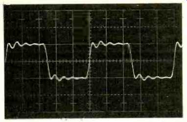
Fig. 10--Square wave response of the amplifier at 10 kHz measured at 10
V peak-to-peak with a 2 uF capacitor load. Vertical scale is 10 V per division;
horizontal scale is 20 uS per division.

Fig. 11--Sine wave response of the amplifier at 20 kHz with 2 dB of overdrive
measured with an 8-ohm load. Vertical scale is 25 V per division; horizontal
scale is 10 uS per division.
To test the amplifier for distortion, it was decided to abandon conventional total harmonic distortion (THD) measurements and investigate only the intermodulation distortion (IM) characteristics of the circuit. This is because THD measurements only identify distortion components which are harmonically related to the test frequency, and these components often lie outside the audible frequency band. Thus, some THD specifications can be meaningless, particularly those made above 10 kHz. The most audible and annoying distortion is not harmonically related to the signal frequency.
This type is called IM distortion, and it is generated when two or more signals with different frequencies interact inside the amplifier to produce what are called intermodulation products. The ear is most sensitive to IM distortion because, by definition, it is non-harmonically related to the signal, whereas THD is.
Two types of IM measurements were made on the amplifier. These were the SMPTE IM measurement and the DIM 100 measurement. The SMPTE IM standard, written by the Society of Motion Picture and Television Engineers, is a measurement technique that identifies static distortion mechanisms, i.e. those that are dependent only on the amplitude characteristics of the signal. Crossover distortion is an example of static distortion, and the SMPTE IM test is extremely sensitive to it. A good discussion of this test and its implementation is provided in [12]. The SMPTE IM distortion of the amplifier was measured with a Crown IMA intermodulation analyzer which uses two simultaneous sinusoidal test tones, one at 60 Hz and one at 7 kHz with an amplitude ratio of 4 to 1. The IM distortion is determined by measuring the percentage amplitude modulation on the 7-kHz tone caused by the larger amplitude 60-Hz tone. The measurement results are shown in Fig. 3. At 250 watts into 8 ohms, the IM level of the amplifier was 0.054 percent. At lower levels, it decreased to 0.004 percent at 800 milliwatts, increasing below that level.
Noise in the measurement system had a strong affect on the low-level distortion measurements, and the data in Fig. 3 have been corrected for it. The upper curve in this figure is the rms difference between the distortion and the residual noise, and the lower curve is the algebraic difference between these; the actual distortion should lie somewhere between the two curves. The residual noise was determined by turning the level of the output signal on the IMA analyzer to zero and recording the percentage distortion reading on the analyzer meter. It was determined that the source of this noise was the analyzer, for the percentage distortion dropped to zero when the phono input jack on the amplifier was short circuited, indicating the noise was not being generated by the amplifier. There is no evidence of crossover distortion in the IM measurement data. This would have shown up as a large peak in the IM level in the critical power range from 10 milliwatts to 1 watt. (Author's Note: The noise was later traced to improper grounding of the IMA analyzer.) The DIM-100 test is one that can be used to identify IM distortion components that fall in the audible range which are caused by distortion mechanisms dependent on both the amplitude and frequency characteristics of the signal. Examples of such distortions are TIM and SID, and this test is extremely sensitive to them. The DIM-100 measurement technique uses a spectrum analyzer to identify and measure the IM components when a square wave and a sine wave are simultaneously applied to the amplifier. Such a measurement technique was originally described by Schrock [13], although no method was given to quantify the measurements. In a later paper by Leinonen, et. al. [14], a method to do this was presented, and the test was called a dynamic intermodulation (DIM) test. It specifies a 3.18-kHz square wave and a 15-kHz sine waved added with the amplitude ratio of 4 to 1 for the amplifier test signal. The square wave is specified to be low-pass filtered with a single-pole filter. The upper -3 dB frequency of this filter is specified to be 30 kHz (DIM-30) for normal testing and 100 kHz (DIM-100) for measurements on the highest class of equipment. This latter test was the one chosen for the amplifier. The percentage of DIM-100 is specified as 100 percent times the ratio of the rms sum of the IM distortion components at the 9 IM frequencies which lie in the audio band to the rms amplitude of the 15-kHz sine wave. These 9 IM frequencies are 0.90, 2.28, 4.08, 5.46, 7.26, 8.64, 10.44, 11.82, and 13.62 kHz. A spectrum analyzer or frequency-selective voltmeter must be used to measure these.
It has been shown that high-frequency THD measurements can be used to identify dynamic distortion mechanisms in operational amplifiers [15]. These tests are also valid in testing power amplifiers but were not used for several reasons, the main one being that the THD must be measured with the amplifier operating near its slew-rate limit. A slew rate of 80 volts per microsecond would require full power THD measurements at 200 kHz and higher, which could damage the output transistors, and the accuracy of distortion analyzers above 200 kHz may not be good. Second, the measurements do not identify IM products that could fall back into the audio range, and these are the distortion components we hear. Finally, THD measurements above the 40-kHz cutoff frequency of the Bessel input filter would require unrealistically large input signals. For example, it would take 56 volts rms at the amplifier input for it to put out a full power sine wave of 45 volts rms at 200 kHz.
Two Hewlett Packard 3310A function generators were used to generate the DIM-100 test signal, and a Hewlett Packard 5381A frequency counter was used to adjust the frequency of each generator to correspond to those specified for the DIM 100 test. An oscillogram of this signal is shown in Fig. 4. Be cause there is no harmonic relationship between the frequencies of the sine wave and the square wave, the oscillogram shows several cycles of the sine wave superimposed on the square wave. The levels were chosen so that the square wave term produced a 100-volt peak-to-peak square wave at the amplifier output while the sine wave term produced a 25 volt peak-to-peak sine wave. The total peak-to-peak signal swing was thus 125 volts, or 1.5 volts less than that of a 250-watt sine wave into 8 ohms. The amplifier output signal when driving an 8-ohm load is shown in Fig. 5. The average power delivered to the load with this signal was 322 watts, which was high enough to cause the load resistors to get quite hot during the test. (A sine wave with the same peak-to-peak signal level would correspond to an average power level of 244 watts.) To determine the DIM-100 distortion components in the output signal, the amplifier output was connected through a variable attenuator to the input of a Tektronix 5L4N spectrum analyzer, and its display is shown in Fig. 6.
Figure 6 shows a spectral analysis of the amplifier output signal displayed over a dynamic range of 80 dB from 0 to 20 kHz. There are seven frequency components in the figure, occurring at 3.18, 6.36, 9.54, 12.72, 15.00, 15.90, and 19.08 kHz.
With the exception of the 15-kHz sine wave term of the test signal, all are harmonics of the square wave term. (The even-order harmonics were caused by an asymmetry in the 3.18-kHz square wave and would be absent with a perfect square wave.) There are no identifiable IM components at any of the nine specified frequencies for the DIM-100 test. The amplifier thus has no DIM-100 components that are greater than-80 dB below the fundamental frequency component of the 3.18-kHz square wave, and the same was true for tests at lower signal levels. It is important to point out that the DIM-100 test does not measure high-frequency IM products lying outside the audible band, so distortion mechanisms which could affect high-frequency THD measurements are not measured. This is because these mechanisms can only affect the sound quality of an amplifier if the distortion components they produce fall back into the audible frequency band--in which case the DIM-100 test will detect them.
Figures 7 through 11 summarize the waveform responses of the amplifier. The 50-Hz and10-kHz square wave responses at 200 watts into 8 ohms are shown in Figs. 7 and 8. The slight amount of tilt in Fig. 7 is caused by the use of 100 percent feedback at d.c. to stabilize the quiescent bias voltages and currents. The waveform in Fig. 8 exhibits the characteristic response of a second-order Bessel low-pass filter, and the upper -3 dB frequency of this filter is 40 kHz. This is low enough so that the maximum first derivative or time rate-of-change of the output signal can never approach the slew-rate limit of the amplifier when reproducing a worst-case signal, which is a full power square wave. The -3 dB frequency is high enough, however, so that deviations from ideal amplitude and phase response below 20 kHz are negligible [3].
Figure 9 shows the 20-kHz square wave response with the signal applied after the Bessel filter. The absence of over shoots or ringing in the waveform indicate unconditional stability with a phase margin that is close to 90 degrees. Thus, the amplifier is not subject to oscillations because of load effects or if the open-loop gain should decrease with age.
The 10-kHz square wave response into a 2-uF capacitor is shown in Fig. 10. This figure reveals only a small amplitude ringing with very little overshoot, indicating outstanding stability of the amplifier into a reactive load. Figure 11 shows the 20-kHz sine wave clipping response into an 8-ohm load.
The input signal overload for this test was 2 dB, and the figure shows a symmetrical clipping characteristic with very little evidence of "sticking." The tests reported in Figs. 10 and 11 are torture tests which, in general, should not be performed by the inexperienced unless the tester is aware of the consequences. The author has seen some amplifiers self-destruct during these tests.
The signal-to-noise ratio of the amplifier was measured with a Bruel and Kjaer 2609 measuring amplifier. With the phono input short circuited to ground, the output noise measured 0.67 millivolts unweighted and 0.174 millivolts "A"-weighted. These translate into signal-to-noise ratios referenced to 250 watts into 8 ohms of 96.5-dB unweighted and 108.2 dB "A"-weighted.
The damping factor was measured by driving the amplifier output terminal from the output terminal of a second amplifier, with an 8-ohm resistor connecting the two. The damping factor is one plus the ratio of the voltage at the output of the second amplifier to the voltage at the output of the amplifier under test. A Hewlett Packard 3575A gain phase meter was used to measure this ratio. At 20 Hz, the damping factor was found to be in the range of 300 to 500, the uncertainty caused by the effects of noise on the measurements. At 20 kHz, the damping factor was 60. It follows that the output impedance of the amplifier at 20 Hz is between 0.016 and 0.027 ohms, and at 20 kHz it is 0.13 ohms. The increase in the high-frequency output impedance is primarily caused by the inductor L1.
Construction details of the amplifier will be provided next issue in Part II.
References
1. Leach, W. M., Jr., "Transient IM Distortion in Power Amplifiers," Audio, Feb., 1975, pp. 34-41.
2. Leach, W. M., Ir., "Author's Reply," Jour. of the Audio Engr. Soc., Vol. 26, No. 6, June, 1978, pp. 453-454.
3. Leach, W. M., Ir., "Relationships Between Amplifier Bandwidth, Slew-Rate Requirements, and Phase Distortion," AES Preprint No. 1415, presented at the 61st AES Convention, New York, Nov., 1978.
4. Leach, W. M., Ir., "Build a Low TIM Amplifier," Audio, Feb., 1976, pp. 30-46.
5. Leach, W. M., Ir., "Build a Low TIM Amplifier-- Part II," Audio, Feb., 1977, pp. 48-56.
6. Meyer, D., "Tigersaurus- 250 Watt Hi-Fi Amplifier," Radio-Electronics, Dec., 1973, pp. 43-47.
7. Millman, I. and C. C. Halkias, Electronic Devices and Circuits, McGraw-Hill, New York, 1967.
8. Bongiorno, I., "High Voltage Amplifier Design," Audio, Feb., 1974, pp. 30-40.
9. Scholfield, M. and G. R. Stanley, "Functional Protection of High-Power Amplifiers," AES Preprint No. 775 presented at the 39th AES Convention, New York, Oct., 1970.
10. Takahashi, S. and T. Chikashige, "Design of High Slew Rate Amplifiers," AES Preprint No. 1348 presented at the 60th AES Convention, Los Angeles, May, 1978.
11. Soloman, I. E., "The Monolithic Op Amp: A Tutorial Study, IEEE journal of Solid-State Circuits, Vol. SC-9, No. 6, Dec., 1974, pp. 314-332.
12. Stanley, G. and D. McLaughlin, "Intermodulation Distortion: A Powerful Tool for Evaluating Modern Audio Amplifiers," Audio, Feb., 1972.
13. Schrock, C., "The Tektronix Cookbook of Standard Audio Tests," Tektronix, Inc., Beaverton, Ore., 1975.
14. Leinonen, E., M. Otala, and I. Curl, "Method for Measuring Transient Intermodulation Distortion (TIM)," AES Preprint No. 1185 presented at the 55th AES Convention, New York, Nov., 1976.
15. lung, W. G., M. L. Stephens, and C. C. Todd, "An Overview of TIM and SID," Audio, June, July, and August,1979.
16. Morrison, R., Grounding and Shielding Techniques in Instrumentation, John Wiley & Sons, New York, 1967.
(adapted from Audio magazine, Apr. 1980)
Also see:
Build a Class-A Amplifier (by Nelson Pass) (Feb. 1977)
Construct a Wide Bandwidth Preamplifier (Feb. 1977)
Transient IM Distortion in Power Amplifiers (Feb. 1975)
Trends for the Future (April 1980)
Crown's Self-Analyzing Power Amplifiers (Feb. 1981)
= = = =