By Daniel Minoli [of International Telephone and Telegraph, Domestic Transmission Systems, Inc., New York, N.Y.]
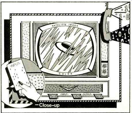
Digital techniques are revolutionizing the high-fidelity industry [1]; this trend is in fact part of a wider phenomenon which is making a marked impact on all signal processing industries (telecommunications, satellite image analysis, pat tern recognition, seismic and radar data analysis, and automatic voice generation, to mention a few).
Digital systems are becoming more and more widespread since the introduction of cheap, reliable, and compact logic (microcomputer) at the turn of the last decade, since this allows storage of the data in a way which can be easily and rapidly accessed, processed and restored. In addition, sophisticated error control techniques allow integrity of the data (and, hence, immunity from noise, crosstalk, fading, and other types of errors).
This series is aimed at explaining the fundamental principles of digital techniques so that the audiophile can have an appreciation of the issues involved. A discussion of the basic architecture of a typical computer is followed by a description of the binary representation of numbers. The key aspects of signal processing in general and PCM in particular also are presented, along with issues in error correction/detection, storage media, editing, and digital and analog-digital-analog discs. Some interesting results are also listed from the mother discipline of digital sound reproduction, namely voice codification, so much used by the telecommunications industry (when one makes a long distance call the voice is actually PCM encoded/decoded on the long-haul network).
Architecture and Operation of a Computer
The operation of a computer is not as mysterious as many people think; we furnish some key facts here, with the goal of setting the ground for the digital data formats to be discussed below. A complete understanding, however, is not required to be able to follow the rest of the article.
A digital computer (i.e. using numbers, in contrast to analog computers which use mathematical functions) is invariably composed of the following units (see Fig. 1): Memory, arithmetic and logic processor, control, and input and output mechanism (I/O). These subunits are interconnected by several lines which provide paths for data, control signals, and computer instructions; the lines are commonly called buses.

Fig. 1--Computer architecture.

Fig. 2--The central processing unit (CPU).
The memory (also referred to as on-line storage unit) stores actual data as well as instructions that tell the control unit what to do with the data. The arithmetic/logic processor temporarily stores data received from the memory and performs calculations and logic operations on this data. The arithmetic/logic processor contains one or more registers which, in turn, contain the data being operated on as defined by the instruction.
The control unit, as its name implies, controls the flow of data in the system, fetches instructions from memory, and decodes the instructions. The control unit executes instructions by enabling the appropriate electronic signal paths and controlling the proper sequences of operations performed by the arithmetic/logic and input/output units. Finally, it changes the state of the computer to that required by the next operation.
The input/output unit provides the interface and, in some systems, buffering to peripherals connected to the computer, transferring data to and receiving data from the outside world. The control unit and the arithmetic/logic processor units with registers are referred to as the central processing unit (CPU) [2]. For now we can think of the memory as a city, where each dwelling (memory location) has an address or telephone number; by specifying the address we are able to focus uniquely into one of these cells and read out the current content or store a new item of data.
Let's look at the CPU in closer detail to obtain insight in the computation process. The basic elements in the CPU are the instruction register, the decoder, the control unit, the program counter, the adder and comparer, the accumulator, and the status register. The block diagram in Fig. 2 illustrates how these elements are interconnected.
A typical processing cycle can be divided into two sub-cycles: Instruction or fetch cycle and execution cycle.
The following chain of events takes place during the fetch cycle: (1) The control unit fetches memory address n from the program counter; (2) the decoder decodes this address; (3) the control unit logic fetches the contents A of memory word n addressed; (4) the control unit logic interprets memory word n as an instruction (not data) and loads instruction A into the instruction register; (5) the control unit logic increments the program counter by 1 for the next cycle (the counter therefore acts as a memory address pointer), and (6) the control unit fetches the contents of instruction register A and decodes the instruction.
The control unit is now ready to implement the second sub-cycle, the execution cycle. The steps followed in the execution cycle depend on the type of instruction to be executed. One of the common instructions is addition or ADD. A typical ADD instruction is based on the following sequence of steps: (1) A piece of data arbitrarily designated "a" stored in memory location m+n is added to the contents of the accumulator. Assuming that the previously stored quantity in the accumulator is "b," the new amount after addition will be a+b, and (2) the new contents of the accumulator are stored in location m+n, which will now contain a+b [2].
One of the greatest steps forward in computer evolution was not explicitly distinguishing the format of the data from that of an instruction. Let us clarify this with an example.
Assume that we have a computer with 15 memory locations (1, 2,...15). When we are talking about instructions, let 01XX mean add (01) what is in memory location XX to the current value in the register; 02XX is multiply, 03XX divide, 04XX sub tract, 05XX read memory location XX and put it into the accumulator, 06XX copy the accumulator into memory location XX, and 07XX print the memory location XX on a piece of paper. For example 0513 means read memory slot 13 and bring it into the register. On the other hand, when we talk about data, 0513 is the number 513. Assume also that each memory location allowed room for four decimal digits (i.e. 00 to 9999), and you've got yourself a fancy calculator.
The program loaded in the memory in Fig. 3 brings the content of location 11 (4444) into the register (working area, scratch pad), adds the content of location 12 (112), stores the results into location 13 (which must be empty otherwise what is there is over-written), brings such result back into the register, divides by 2 (content of memory location 14) and then, after storing the final result in location 15, prints it out.
Note that at the top (program storage area) 112 means add to content of location 12, while at location 12 it means the number 112. The control here does basically two things; it directs the data in the right spot like a policeman directing traffic, and it augments the instruction counter, which in effect provides the continuity of activity. Thus, in a subcycle the next "instruction" is fetched, as soon as the old one is executed, and put into the control, which then decides what to do (which doors to open); the ALU actually performs the required computations.

Fig. 3--Example of a computer.
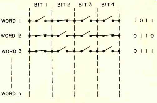
Fig. 4-A relay-based memory.
And so you've got yourself a computer. You have memory addresses, instructions (the collection of instructions is called the instruction set), I/O instructions (e.g. "print"), register, and all the other key components of a real computer.
Memory Architecture
Now that we know how a computer works (or roughly), let's take a closer look at the memory. There are two functionally different types of on-line (always directly and quickly accessible) memory: Read Only Memory (ROM) and Random Access Memory (RAM) by which one means that all cells are equally well (randomly) accessible; their functional purpose should be evident from the nomenclature. These memories are usually accessible in nano-seconds, or at worst microseconds, and can store (in a typical minicomputer) 120,000 or 500,000 words (instructions or data items).
In addition to this easily available memory (the computer can perform one instruction, that is fetch plus execution, usually in nanoseconds or microseconds), one has bulk storage--say up to 120 million items of data. However fetch from bulk storage takes in the millisecond range (fixed head disk) to seconds (tape); this interval is a very long time for the computer (it could have performed a million operations while it was idling waiting for the data). Fortunately once the data header is found, the transfer rate is very high so a large block of data can be brought in virtually in no additional time.
But how does a memory work? From an engineering point of view, the simplest (and hence most efficient) way to store data is to use a dichotomous or binary approach (Boolean algebra and related disciplines can then be used directly). In other words, we want our system to be able to recognize (read) and create (write) two symbols, say an "A" and a "Z," or a "WHITE" and "BLACK," or more conventionally a "0" and a "I," or also a "presence" and "absence" of something, or finally "+5" volts and "0" volts. It's like asking a legally blind person just to distinguish between light and darkness rather than expecting him to see every detail of the world around. Our computer is the legally blind individual; it can only see a 0 or a 1. After all, a computer is only a machine and we can't expect it to understand the details (many symbols). Everything it sees is by inference, not actual sight.
While some computers are based on an octal (8) or hexadecimal (16) system, the fundamental logic is still binary (0, 1).
The dichotomous nature of the storage is easily implementable via elementary physical processes. For example, a magnetized pellet (or bubble or core) (1) vs. a non-magnetized pellet (0); this is the principle of core memory. A charge on a device (1) versus no charge (0) is the principle of charge-coupled devices; a saturized magnetic strip on a tape (1) versus a zero magnetization field (0) is the principle of magnetic tape; a hole on a paper tape (1) vs. no hole (0)--paper tape; a closed relay contact (1) vs. an open contact (0)--first computer--see Fig. 4. All these storage techniques are robust in the sense that it is very improbable that the data become corrupted. It is very improbable that a hole would be punched in the right spot on a piece of paper; it is very improbable that a saturation on the tape would develop, even if a mild (stray) magnetic field nearby influences the tape.
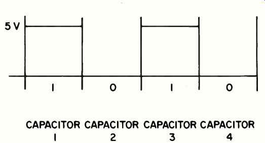
Fig. 5--Example of a memory.

Fig. 6- Robustness to fluctuations in time/speed.
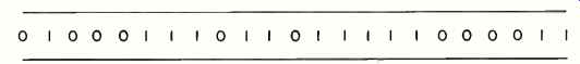
Fig. 7--Serial bits on a tape (idealized).

Fig. 8- Bit map for memory of Fig. 3.
The robustness is implemented via a threshold technique.
Consider a set of capacitors, where we assume that 0 V represents 0 and +5 V represents 1. Then the usual technique is to say that if the charge is between +2.5 V and (say) 20 V, we have a 1; if the charge is between +2.5 V and (say)-10 V, it is a 0. Imagine that the computer writes in a memory, as in the example above, the number 1010 by storing +5 volts in capacitor 1, 0 volts in capacitor 2, +5 volts in capacitor 3, and 0 volts in capacitor 4. See Fig. 5. Assume now that some noise and leakage occurs, so that after 10 minutes the actual readings are 6 V, 1.3 V, 4.2 V,-0.5 V; the threshold approach shaves off or reshapes the signal, on reading, to interpret this combination as 1010. In a real memory such "refreshment" (i.e. reading and resetting the memory to the precise nominal value) is done automatically and constantly (say 10,000 times a second); this refreshment is one of the responsibilities of the memory, and circuitry is built in to take care of itself. In addition to this intrinsic robustness, we also have, right on the memory, error detection/correction algorithms (hard ware) to further insure integrity (see below).
The robustness is also intrinsic in the way the data are read, say off a magnetic disk. Assume that the disk is spinning and at some clock time the material is tested for the bit content (say saturated vs. non-magnetized). Equivalently one can think of a stationary data stream, but with a clock which initiates the read. See Fig. 6. If the disk were spinning at the precisely engineered specification, the bits would be read correctly at the center of the signal, and even if the speed varied or fluctuated somewhat (or if the read clock/crystal was not perfect), the correct bit pattern would still be read as the lower part of the figure clearly indicates.
A few final facts about computer memories before we go on. To have access to the memory, an address must be sup plied (practically a memory is a one-dimensional string of values, i.e. a long list of numbers; see Fig. 7). One must specify the offset (location) from the head (position D) where the item of interest is to be found or written. Magnetic on-line memory (remember tape is not considered on-line memory) was common a few years ago; today semiconductor memories are catching on very rapidly because of their excellent density. On a 1/2-inch by 1/2-inch chip you can store up to 120,000 0s or 1s--equivalent of 16,000 numbers as we will see below; two chips can store this entire article.
These are memories for which read or write is equally possible (read and write instruction time is equal and small); other memories such as optical microphotograph techniques have extremely high densities but the writing is impossible (consider microfilm) and/or access is limited to sequential, rather than random in which you go directly to any address you want to. In other words, for a sequential memory to get to location n, you must first read location 1,2,...n-1. While this is a stringent limitation for computer applications, it is actually ideal for video discs or PCM discs operating on the same principle.
Binary Representation
We have seen that the best way to store data is to use 0s and 1s. The question is: How do we translate everything we are familiar with to 0s and 1s? Well, think of the Morse code, dash = 1, dot = 0, and you have got it. Since for this article we are interested only in coding numbers, we avoid dwelling on the issue of how to code alphabet letters (for those who are interested, research the ASCII code).
Here is the technique. First assume that the largest integer you are ever interested in is M. (For example: Don't worry if a form asking for your net worth has only 6- boxes to the left of the decimal; if you had more then $10 million you would have other things to worry about). Then you will need S "bits" to code that number (a bit is a 0 or a 1)
with S = [log2 M]
and [ ] the ceiling function, or for those who don't know what this is, get S as follows: Divide M by 2; divide what you get by 2, divide what you get by 2, and so on until you get the first number less than 1; S is the number of divisions you performed. Example: If M = 33, then S = 6; 33/2 = 16.5, 16.5/2 = 8.25, 8.25/2 = 4.125, 4.125/2 = 2.0625, 2.0625/2 = 1.03, 1.03/2 = 0.50. A code based on six bits would represent 33 (actually would be good up to 63); now that we know the length of each "word" needed to perform operations on numbers of size up to 33, we need to know how to assign all the codes we get, 100000, 000001, 101010, 011101, 111111, etc., to the numbers.
Here is the technique: When we speak about numbers in the usual or "decimal" representation (1,2,3,...) and say 4732, we really mean
4732=4x1000+7x100+3x10+2
or, how they taught us in elementary school, we have thou sands, hundreds, tens and units. More precisely, we have
4732 = 4 x (10 x 10 x 10) + 7 x (10x10)+3x(10)+2x(1).
Note that the 10 keeps popping up; that's why we call it decimal.
Finally if we let 10^n = 10 x 10 ... x 10, n times, a mathematically precise representation is
4732 = 4 x 10^3 + 7x10^2+3x10^1+2x10^0.
Now when we want to code a number in binary code we use the same (unique) procedure; we set
M=C1x2^s-1+C2x2^s-2+C3 x2^s-3 + ... +Cs+1x2^0.
For example, consider 33:
33=1 x2^5+0x2^5+0x2^3+0x2^2+0x2^1+1x2^0 or 100001 (remember 2^0=1).
Another example:
63=1x2^5+1x2^4+1x2^3+1x2^2+1x2^1+1x2^0 or 111111.
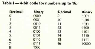
Table 1--4-bit code for numbers up to 16.
And now you've got binary coding. Precise techniques exist for obtaining the constants Cs directly but we shall not discuss these here. Table 1 depicts the code up to 16. The memory of Fig. 3 would now really look like that of Fig. 8.
But how do we perform operations in this coded environment? We must answer: Extremely simply. We consider only multiplication. Remember the multiplication table from elementary school, 100 items to be remembered? 1x1, 1x2, 2x1, 2x2,..., 9x9, 10x1, 10x2. Well, here (remember the computer is legally blind--how much can we expect from it?) we must teach the computer the following simple multiplication table.
| x | 0 | 1 |
| 0 | 0 | 0 |
| 1 | 0 | 1 |
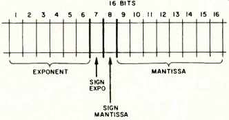
Fig. 9--Floating point notation.
Yes, that is all. (Well, except that before you can multiply you must also know how to add to take care of the carry. Take it for granted: 0+1=1, 1+0=1, 0+0=0, 1+1=10.) Now consider the following:
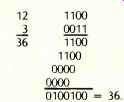
Thus, you do your multiplication the usual way, but when it comes to adding 1+1 you get 10; write 0 and carry 1.
Floating Point Numbers
There is a clear need to work not only with integers, but also with fractional and/or negative quantities. A representation technique for these numbers is referred to as floating point representation. Many variations on a basic theme exist; the key approach is to represent all numbers with a standard template consisting of four parts as in Fig. 9. Here we have a mantissa, the sign of the mantissa, the exponent, and the sign of the exponent. For example, 3/512 and the template of Fig. 9 (which is actually a statement of how powerful the computer in question is) give:
0010011011100000011
since 1/512=1x2^-9 and 9=001001,-=0, +=1, 3=00000011.
With this template, we can represent numbers between 2^- 59 to 2^59 (or 5.7x10^17 to 1.7x10^-18).
Note also that we have 8 binary significant digits (this implies truncation for such things as 1/3=0.333333.... With this system, integers between 0 and 28 can be represented exactly; beyond that one gets truncation or the so-called "scientific notation" in the base 2.
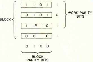
Fig. 10--Block parity.
Error Correction
Various techniques for error detection/correction at various degrees of reliability and overhead exist. We illustrate only two such error detection schemes; correction is more difficult in the audio context we have in mind. In general, correction is done by asking the computer to re-read a block of data or retransmit such block; hence the computer industry has stressed the detection issue (to achieve specific "un detectable error rates") and usually relied on a retransmission protocol (hand shake) to achieve the correction.
The simplest schemes are word and block parity. (Refer to Fig. 10). In this case one counts all the 1s in a word of real data, and (say we are in an even parity scheme) if this number is odd, a 1 is placed in the parity bit so that the total number of 1s is even. If the number of 1s is already even, a 0 is placed in the parity bit (similarly for odd parity). One thus must add one extra bit to the code (this means using up more space, getting less out of the space you have); for our earlier example of a six-bit code to represent 33, we would have to accept 7-bit code.
For example, suppose the data were 111001, then the code with detection capabilities is 1110010; if the data were 111000, then we have 1110001. (Note that the parity bit is the last bit; this bit must not be considered when we use the 2" expansion described above). The detection would work as follows. Assume that the stylus of a fully digital audio system (as the one to be introduced by Philips) picked up the sequence 1110000 and passed it along to a CPU for conversion, etc. But the computer, on checking the parity bit (adding up all the 1s in the word) would have noticed that an intrinsic error existed since in even parity the sum of 1s must always be even. Thus the CPU could instruct a re-read, etc.
The 1-bit parity approach allows the detection of only 1-bit flip, or 3-bit flips, etc., but could not guard against 2-bit flips.
Assume that the original word was 1100110, then if the CPU sees 0100110, it knows we have an error (1 flip). If it sees 0010110, it reaches the same conclusion (3 flips). But if it sees 0000110, it can't tell. This is not a flaw in the system, it is only the degree of checking you get for the price (of adding a single bit). If we assume statistical independence among the bits (this is not always a good assumption), the probability that this technique will fail to detect an error is better than one in 10 million. For its simplicity, this scheme produces remarkably good results, and this is why it is frequently used.
Figure 10 also depicts block parity bits; this is obtained by calling n words a block (n = 4 in this case) and then counting the number of 1s vertically and horizontally; this is why these schemes are also called horizontal and vertical parity checks.
This scheme also allows the correction part (if only one bit becomes corrupted). Assume that the bit marked * had flipped but we didn't know it yet. The third horizontal check indicates an error somewhere in the third word; the second vertical check indicates an error in the second column; it is now possible to achieve the correction.
In general, one can obtain any degree of protection by paying the appropriate price in bits. For example, we can leave two bits of the end of each word and obtain the sum of 1s modulo 3; this is either 0, 1, or 2 (thus two bits since 2 = 10). Here we have more protection.
Next month we'll start with a look at signal processing techniques and how they have been applied to speech for telephone transmission.
Next: Digital Techniques in Sound Reproduction-- Part II (May 1980)
References
1. Stock, Gary, "Digital Recording: State of the Market," Audio, Dec., 1979, pp. 70-76.
2. Weitzman, C., Minicomputer Systems Structure, Implementation and Applications, Prentice-Hall, 1974.
3. Bayless, T. et al., "Voice Signals: Bit-by-Bit," IEEE Spectrum, October, 1973, pp. 28-34.
4. Blesser, B.A., "Digitization of Audio: A Comprehensive Examination of Theory, Implementation, and Current Practice," Jour. of the Audio Eng. Soc., Oct., 1978, Vol. 26, No. 10, pp. 739-771.
5. Flanagan, I.L., "Speech Coding," IEEE Trans. On Comm., Vol.com -27, No. 4, April, 1979, pp. 710-737.
6. Stockham, T., "Records of the Future," Jour. of the Audio Eng. Soc., Dec., 1977, Vol. 25, No.11, pp. 892495.
7. Rhoades, B., "Digital Impact at SMPTE and AES," Broadcast Engineering, Feb., 1979, pp. 60-63.
8. "He is making Caruso sound like Caruso," News in Perspective, Datamation, March, 1977, pp. 168-171.
9. Consumer Guide to 1980 Stereo Equipment.
(adapted from Audio magazine, Apr. 1980)
Also see:
Dr. Thomas Stockham on the Future of Digital Recording (Feb. 1980)
Telefunken Digital Mini Disc (June 1981)
= = = =