
The device shown in Fig. 1 and above is a measurement tool with which you
can properly evaluate the signal-to-noise performance of your hi-fi preamplifiers,
power amplifiers, integrated amplifiers, or any other signal-processing equipment
that operates in the audio-frequency range.
Signal-to-noise ratio measurements are generally made by measuring the output voltage of an audio device with no input signal, and comparing this voltage to the output voltage normally present when the unit is properly driven. However, there are a few factors which complicate this simple technique. First, the noise output of modern hi-fi equipment is so low that it will not register on most a.c. voltmeters. Second, even sensitive a.c. voltmeters have input noise levels of their own that are high enough to obscure the measurement of extremely good audio equipment. Third, S/N ratio specifications published by audio manufacturers are determined from weighted measurements, i.e., just the noise within a certain frequency range is measured. Therefore, what M.J. Salvati you need (besides an a.c. voltmeter) is a preamplifier of known gain and extremely-low internal noise to boost the noise output of the audio equipment under test to a level readable on an ordinary voltmeter, and a filter network that will duplicate the weighting used by the manufacturer. The device described in this article does exactly this.

Fig. 1--The measurement tool for evaluating the S/N performance of today's
high fidelity signal processing equipment.
Theory of Operation
The device consists of two main sections, a low-noise preamplifier and a filter. The preamplifier boosts the level of the signal (noise) being measured to a level high enough to provide a readable voltmeter indication and to negate the effects of filter and voltmeter internal noise. The filter passes only those noise components within specified, selectable pass bands.
Preamplifier Capacitor C1 couples the input signal from jack J1 to transistor Q1. This transistor and transistor Q2 form a d.c.-coupled, negative feedback complementary pair with an open-loop gain of about 4000. Feedback through pot R9 and resistor R5 sets the closed-loop gain at 40 dB (100X). The gain throwaway of 400 stabilizes the closed-loop gain and makes the gain essentially independent of transistor characteristics and battery voltage. Further d.c. stabilization is provided by deriving the bias voltage for transistor Q1 from the junction of resistors R10 and R11.
Pot R8 sets the d.c. output voltage of the preamp at zero. Pot R9 provides fine adjustment of the feedback so the preamp gain can be precisely adjusted to 100X. Diode D1 protects the input transistor from negative-going input spikes. Capacitor C2 adjusts the upper -3 dB point of the amplifier passband to 100 kHz, and provides high frequency stability (phase margin). Switch S1 allows the preamp to be energized independently of the filter section.
Filter Section
The Input terminals of the filter section go directly to filter network #1. This network (whose exact configuration depends on the option you choose) forms various RC high-pass filters in conjunction with resistor R17. These HP filters determine the lower -3 dB corner frequency of the filter-section passband. It is the lower corner frequency that constitutes the main difference between the A, B, and C weighting networks.
The C network has a 20 Hz corner frequency and a 6 dB per octave rolloff rate. The B network has a 160 Hz corner frequency and also has a 6 dB per octave attenuation rate. The A network consists of two cascaded filters each having a 280 Hz -3 dB corner frequency. This provides an overall -3 dB point around 800 Hz and a 12-dB-per octave ,rolloff rate, so the A network really wipes out low-frequency noise components.
Dual FET Q3 forms a high-impedance, unity-gain buffer to drive filter network #2. Transistor section Q3A is a source follower; section Q3B is a constant-current source for Q3A. By using matched source resistors (R13 and R14), the d.c. output voltage of the buffer is zero.
The capacitor(s) in filter network #2 forms an RC low-pass filter in conjunction with resistor R15 and the output impedance of the buffer. This LP filter establishes the 10 kHz upper -3 dB corner frequency characteristic of the A, B, and C weighting networks.
An operational amplifier connected as a unity-gain follower serves as the output stage so the filter can drive low-impedance loads when necessary. Switch S2 allows the filter section to be energized independently of the preamp.
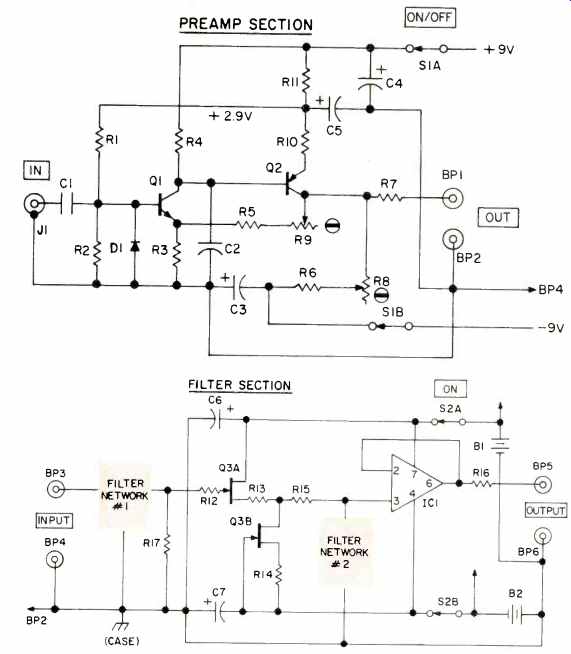
Fig. 2--Schematic diagram.
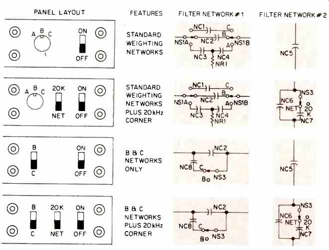
Fig. 3-Weighting network filter options.

Fig. 4-Inside view with the protective metal cover removed.

Fig. 5--Test setup for S/N ratio measurements.
Construction Notes
Options
The first thing to do before buying parts is to decide what you would like in the way of combinations of filters and connectors. The left-hand side of Fig. 3 shows the physical layout of several possible filter sections; the right-hand side of Fig. 3 shows the corresponding schematic.
When you decide which filter combinations you want, insert the schematic section of Fig. 3 into the corresponding spaces in the main schematic (Fig. 2) for a complete customized schematic.
The input connector must be a fully-shielded connector like an RCA phono jack (specified) or a BNC connector (as on author's version). The other connectors can be nearly anything you prefer; the author's version uses double 5-way posts for maximum convenience.
Parts Standard transistor radio batteries are adequate for hobby, service, and most lab applications. However, for critical lab applications where extreme a.c. & d.c. stability is important, use 8.4 volt mercury batteries.
Network capacitors NC1 and NC8 are not standard values. They are "made" by connecting in parallel the standard-value capacitors indicated in the Parts List.
For home use, or other applications where precision is not needed, wider tolerance resistors (5%) and capacitors (10%) can be substituted for the precision parts specified in the Parts List.
Construction the size of the case depends on the amount of panel space needed to accommodate the switches and connectors used on the option you build. The actual circuitry occupies very little space, as you can see from Fig. 4. The largest thing inside the case is the pair of batteries.
However, the case must be one that completely encloses the circuitry in metal; plastic cases or open-ended metal boxes are no good. (The author's unit shown in Fig. 4 has a metal cover that fits tightly over the open side.) The labeling of the filter-section switches can be handled in either of two ways. In Fig. 3, the identification of switch positions is by network designation. This is preferable for audio applications. In my unit (Fig. 1), the switch positions are identified by frequency. This is preferable when the unit is used for other applications besides audio work.
Parts Availability
The Sony transistor types I used in my unit are available from Sony Parts Distributors throughout the nation. However, there are several less expensive American made transistors with suitable noise characteristics. The 2SC1632-xx48 can be replaced by the Motorola MPS A18 and 2N5089. The first substitute is especially recommended since it has the lowest noise figure I've yet seen.
The 2SA705 can be replaced by any good small-signal PNP transistor such as the 2N4058 or 2N5087. The 2N3957, 2N5087, and 2N5089 are available from Ancrona Corp., P.O. Box 2208, Culver City, Calif. 90230.
=============
Table of Specifications

Gain
Frequency response
Input impedance
Output impedance
Max. input level
THD Cd max out
Noise rti (50-ohm source)
Power required
Gain
Input impedance
Output impedance
Max. input/output level
THD Ca 2.5 V out
Noise rti
Power required
Preamp Section
: 40 dB (100X)
: 2 Hz - 100 kHz (-3 dB)
: 100 kilohms
700 ohms
: 15 mV rms
: 0.15 percent
: 0.5 µV over 20 Hz 10 kHz bandwidth
0.65 µV over 20 Hz 20 kHz bandwidth
1.1 µV over 10 Hz 100 kHz bandwidth
: 1.1 mA C4 9 volts
Filter Section
: 0 dB (1X)
: 100 k-ohms
: 50 ohms
: 5 V rms
: < 0.007 percent
: 9 pV over 157 kHz bandwidth
: ± 2.5 mA Ca 9 volts
=============
Adjustment & Calibration
The filter section requires no calibration or adjustment. For the pre amp section, proceed as follows: Adjustment Connect a d.c. voltmeter to the Out terminals of the pre amp section. Two minutes after setting S1 to On, adjust pot R8 for a meter indication of 0 ±0.1 volt.
Calibration
Connect an audio oscillator to the In jack of the preamp section, and adjust the input level to 10 mV rms as indicated on an a.c. VTVM. Then connect the a.c. VTVM to the Out terminals of the preamp section and adjust pot R9 for a meter indication of 1V rms.
Use
To measure S/N ratio with this device, assemble the test setup shown in Fig. 5. Energize all of the equipment and proceed as follows:
1. Set up the controls of the amplifier under test for the input you wish to test. Insert shorting plugs into that input.
2. Connect a short piece of wire between the red preamp Out and red filter Input terminals.
3. Set the filter network switches to the network (A, B, or C) specified in the manufacturer's literature for the input under test.
4. Adjust the voltmeter range switch for a near full-scale meter indication.
If the reading is 1.0 volt or less, calculate the S/N ratio as follows: S/N ratio (dB) = 20 log 100 x Rated output voltage
Step 4 voltage
5. If the indication in Step 4 is over 1.0 volt, disconnect the wire jumper installed in Step 2 and move the cable at the preamp In jack to the filter Input terminal.
6. Readjust the voltmeter range switch for a near full-scale meter indication. Calculate the S/N ratio as follows:
S/N ratio (dB) = 20 log Rated output voltage
Step 6 voltage
If you built one of the options with selectable upper corner frequency, you can also measure the S/N ratio over the traditional audio passband (20 Hz 20 kHz) by setting the network switch "C" (to set the 20 Hz lower corner) and the 20K/NET switch to "20K" (to set the 20 kHz upper corner).
==============
PARTS LIST

Reference Designation | Description
Q1 Q2 Q3 IC J1 BP1,BP3,BP5 BP2,BP4,BP6 S1,S2 B1,B2 D1 R1 R2 R3 R4 R5 R6 R7,R16 R8 R9 R10 R11 R12 R13,R14 R15 R17 C1 C2 C3,C4,C6,C7 C5
SONY 2SC1362-xx48 NPN transistor (see text)
SONY 2SA705 PNP transistor (see text)
2N3957 or 2N3958 dual FET 741 integrated circuit, TO-5 or DIP-8 case RCA phono jack (Switchcraft 3501FR) Red 5-way binding post Black 5-way binding post DPST slide switch
9-volt transistor radio battery
High-frequency silicon diode (1N914, 1N4148, etc.) 470 kilohm 1 percent 1/4W metal-film resistor (Dale CMF-65)
150 kilohm 1 percent
1/4W metal-film resistor (Dale CMF-65)
1000 ohm 5 percent 1/4W carbon resistor
68 kilohm 5 percent 1/4W carbon resistor
91 kilohm 5 percent 1/W carbon resistor 8200 ohm 5 percent 1/4W carbon resistor 51 ohm 5 percent VIW carbon resistor 2.2 kilohm trimmer pot 22 kilohm trimmer pot 100 ohm 10 percent 1/4W carbon resistor 6200 ohm 5 percent 1/4W carbon resistor 4700 ohm 10 percent 1/W carbon resistor 1000 ohm 1 percent 1/4W metal-film resistor (Dale CMF-65)
33 kilohm 1 percent 1/4W metal-film resistor (Dale CMF-65)
100 kilohm 1 percent 1/4W metal-film resistor (Dale CMF-65)
0.68 µF 100V mylar capacitor 330 pF 5 percent mica or ceramic capacitor 10 µF 16V electrolytic capacitor 47 µF 6.3V electrolytic capacitor 12 x 21/2 x 21/4 aluminum case (see text) 9V battery connector (2 req.)
=================
(Source: Audio magazine, May 1977; M.J. Salvati)
= = = =