|
|
Is it time to update your signal generator? Follow these tips from an audio expert.
I use an intermodulation distortion (IMD) signal generator based on the FET-based design by Erno Borbely. It produces a CCIF 19 + 20kHz and a multi-tone (MIM) 9 + 10.05 + 20kHz test signal. It has served me well for the last eight years. The only downside is the noise floor around —90dB. Progress in audio equipment design has made this noise floor the limiting factor in some of my measurements. I also have an occasional need for the CCIF 11 + 12kHz test signal, which my old IMD generator does not produce.
The other problem is its size—a 19” x 12” x 4.5” rack unit chassis. This is because it also contains a steep 80dB 1kHz bandpass filter to isolate the 1kHz IMD product and direct it to an external meter. Ever since I purchased a 16-bit audio spectrum analyzer, I no longer use the 1kHz filter portion of the IMD generator, and with all the other test equipment at my bench, I also wanted a smaller IMD unit.
A lamp-stabilized Wien bridge sine-wave oscillator design has a minimum number of components, and can achieve a low distortion level of 0.0025% One of the weaknesses of this circuit is the higher distortion at low frequencies due to the response lag in the lamp. This would not be a problem in my design because the lowest frequency I planned on developing is 9kHz.
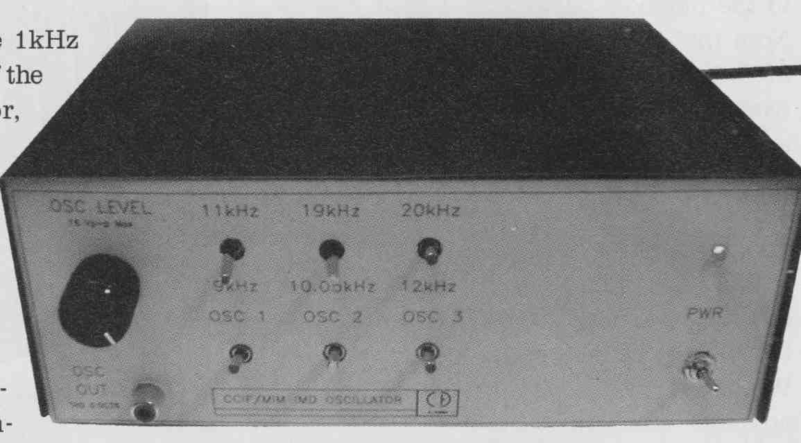
PHOTO 1
Parts cost, including the chassis, is less than $90.
POWER SUPPLY
The power supply for the IMD genera tor circuitry is shown in Fig. 1. The raw supply of ±27V DC is obtained by full- wave rectifying the output of center-tapped transformer Ti and rectifying it with diodes D1-D4. R-C snubber net works are connected across each diode to attenuate transients due to rectifier switching. LED 1 serves as the power-on indicator.
The resulting DC voltages are filtered by C25 and C26, and then applied to linear regulator ICs U5 and U6 to produce power-supply voltages of ±19.8V DC.
I wanted as high an output voltage as possible to drive low-gain amps and preamps. The regulated supply voltage is 90% of the maximum 22Vcc rating of the oscillator op amps, and is my upper limit to ensure long-term reliability. C29 and C30 reduce the output noise from the regulators. Capacitors C3 1 and C32 are the regulated DC output filter capacitors. Diodes D6-D11 protect the linear regulators in case of accidental faults.

FIGURE 1: Power-supply schematic.

FIGURE 2: IMO generator schematic.
The schematic diagram of the IMD generator is shown in Fig. 2. The unit is composed of three low-distortion sine wave oscillator circuits (U1-U3) and summing amplifier U4. Each oscillator provides one of two different output frequencies, and can be disabled when not in use.
Because all three oscillators are identical except for the resistors that determine the frequency of oscillation, I will explain the oscillator at U1. S2 selects between two pairs of matched 1% metal film resistors (R1—R4) that select the tuned frequency. The parallel BC Wien network is provided by the resistors selected by S2 (R1 or R1 in parallel with R3) and capacitor C1. The series BC Wien network is provided by resistor R2, or R2 in parallel with R4, and capacitor C2. These networks provide the positive feedback across UI and the phase shift necessary for oscillation.
The gain of U1 is set by R5 and the resistance of lamp L1. The negative feedback control for gain stability is provided by the positive temperature coefficient of lamp Ii. When power is first applied, the lamp is at its cold resistance of about 87-ohm. The gain is about 4.5, so the oscillator voltage builds up.
As the output voltage increases, the current through Ti increases and so does its resistance. This reduces the gain of U1. With the proper selection of R5, the oscillator establishes a stable operating point, and a low-distortion sine-wave output results. Note that I used a #1819 lamp instead of the more commonly used #327. This is based on my earlier experiments with lamp-based Wien-bridge oscillators.
Each oscillator drives the output inverting summing amplifier U4 through a series select-at-test (SAT) resistor. The exact SAT resistor value is based on the stable oscillator output voltage, which depends on the individual lamp. It is necessary to adjust the gain of U4 to just below its clipping output voltage whether only two oscillators are in use for the CCTF test tones, or all three are in use for the multi-tone output.
Take the case in which the 19 + 20kHz CCIF signal is used. S4 selects the 19kHz tone from U2 and S6 selects the 20kHz tone from U3. S3 is opened and turns off the third (U1) oscillator by disconnecting C2 from the output of U1, thus opening the positive feed back path. This is necessary to prevent crosstalk that would occur if the unused oscillator were left running. S3 also removes the short across R19, so the overall voltage gain of U4 is set to -2.91. This produces an output voltage at U4 pin 6 of 12V RMS.
When all three oscillators are operating for the multi-tone IMD signal, switches S3, S5, and S7 short R19, decreasing the gain to -2.91 to reflect the additional summing voltage component from U1. This reduced gain maintains the output voltage at U4 pin 6 to 12V RMS.
Operating just one of the oscillators at a time produces a single sine-wave output, but at a reduced output voltage of just over 6V RMS since the gain of U4 remains -2.91. This is also the mode used to check the THD, amplitude, and frequency of each individual oscillator.
The IMD output signal is applied across pot R21, and R22 sets the output impedance to 600-ohm. C11 limits the -3dB bandwidth of U4 to 455kHz. The 22pF caps at each op amp are necessary since the 5534A is not stable for gains less than 5 without these compensation caps. Caps C12 through C19 are local decoupling capacitors located at the IC package supply pins.
The circuitry is quite versatile. You can add additional oscillators for other IM measurements such as SMPTE, or even a square-wave oscillator section for DIM testing. The switching will be come more complicated because the gain of U4 will need to be adjusted for each type of IM signal you want to generate, but 3PDT miniature toggle switches are readily available.
CONSTRUCTION
The circuitry makes use of high-quality components to ensure that THD and stability are the best possible. The frequency accuracy depends on how well the oscillator BC network components are matched. Matched pairs of polystyrene caps were selected for each individual oscillator from a large sample of 5% tolerance parts. Similarly, matched pairs of metal film resistors were selected for each individual oscillator from a large sample of 1% parts. Note that R1, R2, R15, and R16 are actually parallel pairs of resistors. These were needed to achieve the exact output frequency to within 0.2%.
Photo 1 shows the front view of the IMD signal generator. The three upper toggle switches select the oscillator frequencies. The lower switches turn the oscillators on or off. The output level control is to the left above the phono output jack.

PHOTO 2
Photo 2 shows a top view of the perfboard that allows all the components to fit within the 8.25 x 6.125 x 3.06”chasiss specified in the parts list. The transformer and rectifier/snubbers are on the right side of the unit with a galvanized steel shield between the power section and the oscillator/amplifier section. I used an IEC line cord receptacle for the AC power. Scrape the paint off the chassis where the green IEC ground wire connection is made. The three lamps are mounted on the rear wall of the chassis with rubber grommets to isolate them from vibration.
Figure 3 shows the mechanical layout of the chassis. The power-supply regulators are on the perfboard. I used star ground and DC supply connections to minimize oscillator crosstalk. The oscillator and amplifier circuits float with respect to the chassis to avoid any ground loops between the IMD generator and the equipment under test.
Figure 4 shows the front panel designations for the switches and controls. Make an exact size copy for use in locating the holes for the components. You can use transfer lettering, or photocopy the figure to scale on a sheet of matte self-adhesive drafting appliqué film as I did. This film is available at drafting and art-supply houses under the brand name Letraset Letracopy Creative or Chartpack DAF8 appliqué film.
A light-color paint (which the specified chassis has) is required since the photocopy lettering is black. Apply the lettered film to the front of the unit in the proper location. Cut through the film at the drilled holes and then spray it with two coats of clear polyurethane for protection.

FIGURE 3: Chassis layout.
= = = =

TABLE 1: PARTS LIST.
ADDITIONAL ITEMS: Perfboard, control knob, nylon spacers, LEO mounting ring, hookup wire, power cord, solder, hardware, and so on. Drafting applique’ film (Letraset Letracopy Creative or Chartpak DAFB) is available at art or drafting supply houses. Other options are Clear Laser Labels by Avery (Various sizun, four-digit part numbers start with #566), BEL Inc. ink jet decals, or Worth Poly polyester laser labels from Worth Data.
= = = =
INITIAL TESTING
Before installing the four op amps, plug in the unit and check for the proper power-supply voltages at the corresponding IC socket pins (+19.8V at pin 7 and -19.8V at pin 4). If all is well, power down the unit (waiting for the power-supply caps to drain) and in stall the ICs. Apply power again and check for oscillation at U1, U2, and U3 pin 6. You are looking for approximately 2.1V RMS from each oscillator. If any of the oscillators do not operate, you may need to adjust the value of R5, fill, or R17. If you have a THD meter, you can also adjust R5, fill, and R17 for minimum distortion.
Next, check all six operating frequencies. You may need to adjust the values of the series and parallel Wien network resistors to achieve the exact frequencies. The three MIM frequencies are more critical because the two lowest even-order and odd-order IM products (950Hz and 1050Hz) are very close together.
Finally, adjust the values of R6, R12, and R18 for any differences in the oscillator voltage amplitude (you could use a cermet pot here, but lamp life should be unlimited because the voltage across the lamp is but a small fraction of its rated voltage). Each individual oscillator should produce about 6.2V RMS at the output jack with the level control at maximum.
The response flatness is very good for the Wien-bridge oscillator, so there should not be any amplitude difference between the two frequencies from any given oscillator.
MEASUREMENTS
Figure 5 shows the 19 + 20kHz CCIF spectrum of my original IMD tester, with its noise floor rising as high as -90dB. Figure 6 shows the same CCIF signal from the lamp-based IMD generator that is the subject of this article. Figure 7 shows the 11 + 12kHz IMD signal, and Fig. 8 shows the 9 + 10.05 + 20kHz MIM signal. The 0dBfs output in all cases is 12V p-p.
REFERENCES
1. "Multi-Tone Intermodulation Meter," TAA 2/89, p. 7, 3/89, p. 13, 3/90, p. 18; Borbely, Erno.
2. "Build your own Audio Oscillator," Popular Electronics 7/97, 9/97, 10/97; Miller, Franklin.
3. " Wien Bridge Based Oscillators," Linear Technology Application Note 43, 1993 Linear Applications Handbook Volume I Figure 39, pp. AN43-29, 30.
4. "Precision Sine Wave Oscillator," Hansen, C., Audio Electronics 5/98, pp. 8-23.
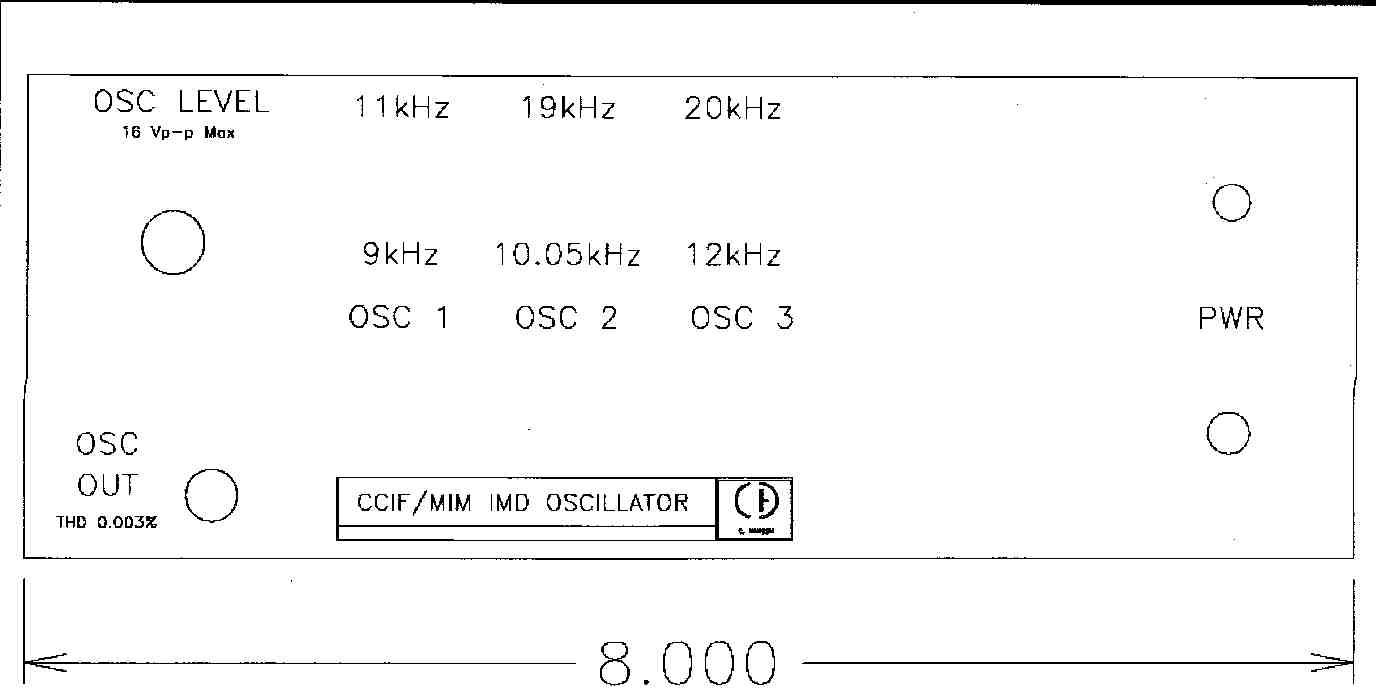
FIGURE 4: Front panel designations.

FIGURE 5: Original MD tester 19 + 20kHz CCIF signal.

FIGURE 6: 19 + 20kHz CCIF signal.

FIGURE 7: 19 + 20kHz CCIF signal.

FIGURE 8: 9 + 10.05 + 20kHz MIM
SUPPLIERS: Digi-Key Corp., Mouser Electronics
============