|
|
(source: Electronic Technician/Dealer, Jan. 1980)
High power audio amplifiers frighten many technicians.
Trouble seems to compound itself all too easily when servicing them. Here are rules and procedures to keep you out of trouble.
By James Sims, CET In the past several years, and in ever increasing numbers, the high powered dc coupled amplifier has been accepted for uses ranging from the home audio system to large rock bands. Here we will discuss the most safe and sure ways to execute repairs.
Basic rules
These repairs can be time consuming and expensive if a few golden rules on servicing techniques are not followed.
Let's assume that a large high powered amplifier is brought into your shop for service with the complaint "it blows fuses as soon as it is switched on." Rule No. 1: Never attempt to power up the amplifier before removing the covers and giving the amplifier a good visual inspection. Look for signs of over -heating. Also check for wiring modifications, possibly for handling extra speakers. Examine the printed circuit boards for signs of cracking.
Some amplifiers which are used by rock 'n roll bands are thrown around a lot.
Rule No. 2: Never switch on the amplifier with any kind of load on its output stage. If you can't see anything wrong after a visual inspection, power it up slowly with NO LOAD. After initial power -up, measure the dc voltage on each speaker terminal and check to insure that both positive and negative power supplies are balanced. If you fin that the supplies are unequal, or any pa of that supply on either speaker terminal switch it off immediately!!
Rule No. 3: When replacing components, be sure that the component you select has the correct characteristics required for the circuit you install in into.
A typical amplifier
Shown in Fig. 1 is an example of a high powered dc coupled amplifier with its covers removed. Notice the split power supply for both positive and negative feed for the output stages. In this case, the power transformer is a toroid. This type of transformer can deliver more power much more efficiently from the source and is usually smaller in size.
Filtering is done primarily by one large electrolytic capacitor for each supply line.
The output stage consists of 12 output transistors, two driver transistors, and two output resistor boards. Six TO-3 power transistors are (as shown) on the top heat sinks and six are below. One driver transistor is mounted on each output resistor board. Notice the two cooling fans. Again, this allows for a reduction in heat sink area and cuts down total amplifier size. Usually these fans are temperature controlled and do not turn on until a preset heat sink temperature has been attained. At that point, the added forced air cooling allows for maximum power dissipation with a reduced risk of thermal runaway.
Equipment and procedures
The test equipment that is required should be found in any service shop.
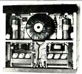
Fig. 1--A typical high power audio amplifier.
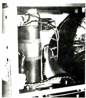
Fig. 2--A corner of the amplifier power supply showing the bridge block.
Here are the essentials needed.
1. Digital volt meter.
2. Variable ac supply with meters [0 Vac to 130Vac ].
3. Oscilloscope-single or dual beam.
4. Four 4 ohm load resistors wire-wound at 100 watts each. Connect for 200 watts per side at 8 ohms.
5. Low distortion audio sine-square generator.
6. A VOM with a good low ohms scale
The easiest method of servicing would be to break up the amplifier into four basic parts:
1) Power supply;
2) Output stages;
3) Driver boards; and
4) Shutdown section.
First of all stabilize all the dc operating conditions, then pass a signal through the amplifier. This may require further troubleshooting with respect to the ac operating conditions. Plug the amplifier into the variable ac source and insure that it is switched off and set at zero.
Power supply
Usually power supply faults are obvious and do not consume much time.
Generally, the components found here are designed to handle great amounts of power and are fairly rugged. If fuses are blowing in the power supply section, check the bridge rectifier block (Fig. 2).
Use your VOM on RX1 and check for shorted diodes. It may be advisable at this time to locate and disconnect any supply line leads which go directly to either output stage. A shorted output device can sometimes cause the supply to appear shorted. Check for signs of extensive heating or burned wiring. The odd time you may run across a defective electrolytic, but this is very rare. Finally, check for poor solder contacts, especially on common grounds. Where grounds are made through a mechanical connection, insure that these are tight.
Output stage
The output stage is responsible for supplying the great amounts of power required for the load (Fig. 3). Shown are six parallel devices on top and another six on the lower portion of the heat sink. Make sure that all supply connections and output connections are tight. A schematic diagram of an even larger output stage is shown in Fig. 4.
Notice that all the output devices are in parallel to insure maximum current.
These output transistors are Q8 through Q17. Any one of these devices may be shorted or "leaky;" so if you change one, make sure you also change its adjacent device. When selecting replacement power transistors, check for differences in gain characteristics and insure that power dissipation and breakdown voltage specifications are adequate.
Resistors R29 through R38 must be carefully inspected for signs of overheating and/or cracking. Use your VOM to check that each resistor is close to its specified value. Insure that both back swing clipper diodes D3 and D4 are not shorted. A biasing voltage is supplied by Q3 which is attached thermally to the heat sink.
Driver Next, we look at the driver boards. This is the heart of the amplifier. The driver board is direct coupled to the output stage and usually trouble on one means trouble on the other. (See Fig. 5.) Shown is an excellent example, for it contains most of the commonly used circuitry.
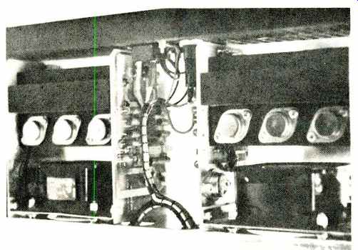
Fig. 3 The amplifier output stages.
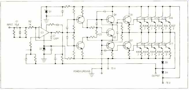
Fig. 4 A high power single channel amplifier, the output stage of which
uses ten power transistors.
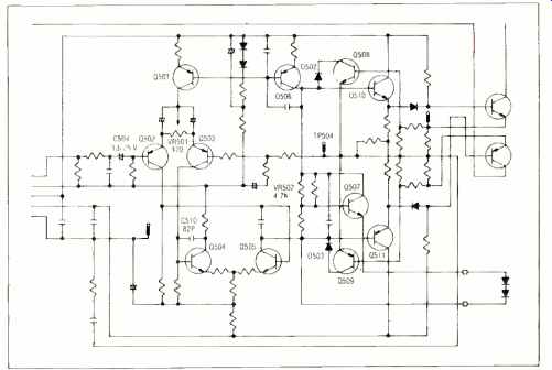
Fig. 5 Typical direct coupled driver stages for a moderately high power
output stage.
There are several important functions of a driver circuit other than the amplification of the input signal.
a) It insures zero dc voltage at the center point (speaker terminals) under normal operating conditions.
b) It supplies the correct amount of dc bias current to the output stage. This normally tracks directly with output stage operating temperature.
c) In most cases, some form of over current shutdown is also employed.
Insure firstly that all power supplies are fully discharged. Next, with your VOM, check the forward and reverse resistances of all diodes, resistors under 1K ohm and transistor junctions. If you have an in-circuit transistor checker, check ALL semiconductors dynamically.
If you are using a VOM, check for shorted collector-emitter junctions or open base-emitter junctions. When changing bad diodes, make sure your replacement is exact. In many cases, diodes in a shutdown circuit are vastly different from those used in biasing circuits. When changing a differential amplifier transistor, always change both, even if the adjacent device is found to be undamaged. One of those devices could be partially damaged from the original fault and go into "second breakdown" after initial run-up, which would surely cause a second repair equal to the first.
It is not worth sacrificing reliability for the cost of one or two more transistors.
Assuming the output stage is now repaired, switch the variable ac supply on and slowly increase the line voltage until approximately 50% of full supply.
Watch for excessive primary supply current and overheating. If either of these two conditions occur, reduce your supply voltage to the point at which input current is reasonable or switch off the power and reassess; you may have overlooked something obvious. While running at 50% of the supply, it should enable you to make all necessary dc voltage measurements. Firstly, check for an excessive amount of dc on the center point or speaker terminal. In this case, that would be test point 504 (see Fig. 5). If an excessive dc voltage is present, its source could be a defective output device, driver device (Q511 and Q510), or defective differential amplifier, here being Q502 and Q503. To help find just which device is causing the problem, determine the dc polarity. This should point directly to either the PNP side or the NPN side of the driver board.
On this driver board (Fig. 5), you are able to make small dc offset voltage adjustments by varying VR501. This pot is found across the two emitters on the input or differential amplifier. A defective bias transistor or bias pot, here Q507 and VR502, could cause overheating of the output stage. If this occurs, switch the amplifier off and replace the bias transistor.
Your attention can easily be distracted working on the input, while a brand new output stage goes up in smoke. This is precisely the reason for not applying a load across the amplifier or running at full line voltage.
One other common driver circuit is that of Fig. 4. Here an operational amplifier is used as an input amplifier.
This introduces many benefits to the circuitry, such as improved slew rate, stable dc offset and source current limiting, which are all features of most operational amplifiers. Here it is best to start at the input. Check both dc supplies for the operational amplifier. These are zener diodes D1 and D2 (Fig. 4). Also check to see that there is no dc voltage present on the inverting input on the op amp via C1 and R2. Transistors Q1 and Q2 provide the voltage gain, while Q4 and Q5 supply the current gain.
To insure proper signal performance, it is necessary to look at both the output stage and driver boards together. After replacing all of the defective devices and checking all of the remaining ones, run your supply up slowly to 100%. Try to pass a 1Khz signal. Watch for premature clipping on one side of the wave. This would also indicate a dc offset voltage present on the speaker terminal. If this is the case, a driver, buffer or output transistor could be breaking down under load, yet check out properly in the quiescent state. When this occurs, a great deal of supply current is drawn and this may blow supply line fuses or actuate any current limiting or shutdown circuits. To help establish just where the current is being sourced, use your digital volt meter and check for excessive voltage drop across any of the output emitter resistors (see Fig. 6). If this does not reveal the source, check the driver transistor currents while passing a signal. It may be necessary to defeat any current sensing circuits in order to find the defective device (see Fig. 5). Here disconnect one end of D502 and D503.
This will disable transistors Q508 and Q509. Remember that you will lose any driver or output stage current limiting, so slowly run the amplifier back up to one-half supply only. Again, refer to Fig. 5. Transistor Q501 serves as a constant current source for the input amplifier.
Insure that this device is not damaged.
If the signal is reasonably symmetrical, yet disturbed, check the collector of Class A driver Q505. This transistor supplies signal for the driver and output stages, and should indicate the source of any distortion. The base of Q505 should also be checked. A severe loss of voltage gain here will certainly produce a poor low level output. Check Q506; this transistor serves as a constant load for Q505.
If the problem is no signal at all, insure that the input amplifier is operating and a signal is being passed via C504. It is possible that excessive voltage was applied directly to the input causing damage to this capacitor and possibly the differential amplifier.
High frequency oscillation could be caused by a loss of any RF suppression capacitors, such as C510 across C504.
Or, as in Fig. 4, C7 from the output to the inverting input of the operational amplifier. Be careful of high level, high frequency oscillations for they tend to cause excessive drive, thermal runaway, and eventual breakdown. Also check for open path of ground foil on the driver PCB or open feedback lines which in turn will cause excessive circuit gain and possible oscillation.
After you are satisfied that the amplifier is operating properly, establish its total RMS output power into an eight ohm load with both channels operating.
Watch for a decrease in input line voltage as your power output increases. Correct for this by resetting the variac to 120Vac. If you do not have any specifications at hand, total output power can be established by measuring either the positive or negative dc supplies. Take this measurement with both channels running just before clipping and use this formula (B +2/8)/3. Remember, this will give you a good close estimate and not an exact specification. For example, when measuring the positive supply voltage with the amplifier nearly at clipping, you will read positive 50vdc.
50 x 50 = 2500 + load impedance or 8 = 312.5 + (converts to approximate RMS value) = 104.16 watts RMS.
In most circuits, there are provisions for setting the center point or output offset voltage and the idle bias. These settings should be checked after the amplifier has warmed up. Set your audio generator to 1 kHz and run the amplifier at approximately 45% of full RMS output. Then make these adjustments slowly and with no input signal.
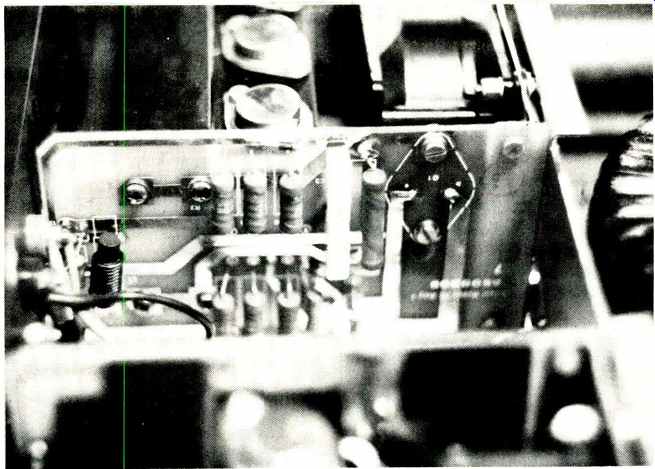
Fig. 6 This circuit board mounts the individual emitter resistor for
each of the paralleled output transistors.
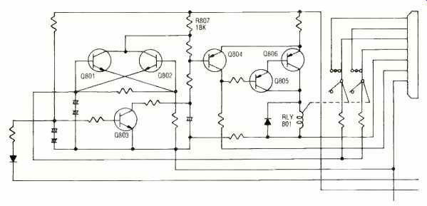
Fig. 7 An overvoltage shutdown circuit, employed to protect the speakers.
Protection circuits
The primary function of these circuits is to protect internal components and external loads after the normal operating parameters of the amplifier have been exceeded. This is done in several ways.
1) Fuse protection. These fuses can be found in the primary of the power transformer, in the secondary ac side or after rectification as B+ and B- fuses.
Fuses may also be found directly in series with each main audio output line.
This limits maximum signal current and protects both output stages and speakers.
2) Over voltage shutdown. (See Fig. 7.) If an excessive dc voltage is produced at the speaker terminal, it enters at the base of Q801. When this voltage is positive, Q801 becomes conductive, and when it is negative, Q802 becomes conductive. As a result, a current runs in R807, decreasing the base voltage of Q804, causing it to become conductive.
This, in turn, shuts Q805 off and the speaker relay opens, insuring that no dc reaches the load. A turn on time delay is also incorporated here to protect the speakers from any high level transients.
3) Over current shutdown. (See Fig. 5.) This is probably the most widely used form of protection. The transistors involved are Q508 and Q509. If a specific value of resistance is placed in series with each base (Q508 and Q509) and the center point, networks R and R'; any increase in output current would cause a proportionate voltage increase across the resistance. This value of resistance is set so as to cause 600mv on each base at maximum specified output current. Q508 and Q509 then become conductive bypassing current from each driver transistor Q510 and Q511. In actuality, both driver bases are pulled together and the output stage current is severely reduced.
Many different variations of these circuits are also used. However, the most protected amplifiers employ all three kinds, as mentioned above. For example, if a shorted speaker were to be used on a dc coupled high power amplifier, the protection would reduce the risk of internal circuit breakdown.
Firstly, the turn on time delay would prevent any high power transients from damaging internal components.
Secondly, when the output relay closed and connected the shorted load across the output stage, overcurrent limiting would reduce the risk of exceeding any maximum current specifications.
However, if one or more power or drive transistors did become shorted, full supply would be felt at the speaker terminal. At this point the over -voltage shutdown would immediately open the output relay and disconnect the load completely. One should remember that these protection devices will not always prevent amplifier failure, but will make the circuitry much less susceptible to human error and component failure.
Finally, when the repair has been completed, explain to the customer that the amplifier is operating now, but will not continue to do so if proper operating procedures are not followed at his end.
Suggest to this customer that he check his speakers and cables, for it is too often that an amplifier is returned repaired and used again under the same set of conditions that caused the original failure.
You can see that by following a few simple precautions and familiarizing yourself with service procedures, a more reliable and profitable repair can be accomplished.