Before the advent of FM there were two main types of receivers on the market, the t.r.f. and the superheterodyne. Both types were used for the reception and detection of a-m signals. So far as these receivers are concerned, it is well known that the superheterodyne has definitely taken over the field, and the t-r-f receiver is outmoded.
Whenever the term "radio" or "receiver" was used, the type of modulation was understood to be AM and very seldom, if ever, was the type of modulation mentioned, especially in referring to the commercial type receiver. The coming of FM changed the method of talking and writing about receivers because either a-m or FM signals may be meant.
Similarities and Differences Between the A-M and FM Receiver
Section 1 briefly summarized some of the similarities and differences between a-m and FM receivers. The three basic types of super heterodyne receivers were illustrated in Fig. 1-15 and are redrawn here for ease of discussion. The a-m superheterodyne receiver illustrated in Fig. 7-1 (A) is of a general type, while two main types of FM receivers are illustrated in Fig. 7-1 (B) and (C). As pointed out previously, the main differences between the a-m and FM receivers are in their methods of detection.
We are more or less familiar with the common methods of a-m detection, such as diode detection, grid detection, and plate detection.
The analysis of these detector circuits is primarily concerned with a modulated signal that is varying in amplitude, and it is these amplitude variations which are to be reproduced. In the FM receiver, the detector circuit and its associated networks must respond to a modulated signal that is varying in frequency and not in amplitude, so their design is completely different. It is the purpose of this guide to analyze in detail only those circuits dealing with FM.
In present-day receivers the three types of FM detector circuits used are the discriminator detector, the ratio detector, and the oscillator detector; these detectors will be analyzed in detail later. The latest detector, the FreModyne, is analyzed on page 413 of the appendix.

Fig. 7-1. Block diagram of conventional a-m and FM superheterodyne receivers.
Note that the difference occurs only after the i-f amplifier stages.
Except for the detector circuits, not much difference can be noted between the a-m and FM receivers in the block diagrams of Fig. 7-1.
However, the r-f, oscillator, and i-f circuits differ as far as their actual physical designs are concerned. If a comparison of the physical construction for both the a-m and FM receivers is made, the r-f coils in the FM receiver will be found to contain as few as one half or one turn of wire in some instances, compared with quite a number of turns in those coils in an a-m receiver. The i-f coils too have correspondingly few turns. This immediately establishes the importance of . FM design as far as wiring and other physical factors are concerned, be cause the added inductance of such wiring and the stray capacitance present might affect the circuit at the FM frequencies and might de tune the set or produce unwanted oscillations.
The primary functions of the r-f, oscillator, and i-f stages are the same in both types of receivers. This is amply evidenced by the fact that many of the combination a-m and FM receivers use the same r-f, oscillator, mixer, and i-f tubes for both AM and FM The associated circuits, however, are different for each type of signal. The selection of the tuned circuits for each type of modulation is made by special switching arrangements within the receiver.
The primary purpose of the audio stage in reproducing the audio intelligence conveyed by the modulated signal is the same in both; FM and AM Many combination a-m and FM receivers use the same audio system, but usually the audio response is not high fidelity to the extent possible with FM In a-m broadcasting the usual maximum audio frequency that can be transmitted is 7.5 khz (due to regulations imposed by the FCC), but in FM audio frequencies as high as 15 khz can always be transmitted. For faithful reproduction of audio signals in either case, the audio stages should be able to pass the maximum audio frequencies involved. A detailed analysis of the audio system is given in a later section of this Section.
One of the greatest differences between an a-m and FM receiver is the effect of interference. Due to the type of modulation involved and the circuits employed, the FM receiver needs a much lower signal-to-noise ratio than the a-m receiver for rejection of noise or other interference. In FM the signal-to-noise ratio required is only 2 to 1, in most cases, whereas in AM it is 100 to 1. This means that in FM the strength of the desired signal need only be twice as great as the interfering or noise signal, whereas in AM the strength of the desired signal must be at least 100 times as great as that of the interfering or noise signal.
In understanding the advantages of minimized interference effects, the nature of the FM signal and the nature of the detector and limiter stages (if any) of the FM receiver are of primary importance. The former was dealt with in the first part of this guide. The transmitted signal, being frequency modulated, has very little chance of changing in frequency or phase due to interference. The greatest change will be in amplitude, since most interference phenomena are amplitude variations. Taking the detector and/or limiting stages of the FM receiver into account, we find that these stages of the receiver will eliminate amplitude variations due to interference.
THE R-F STAGE
As mentioned previously, there often is no difference in the schematic form of the r-f circuits of both a-m and FM receivers. however, if the schematics showed the proportional number of turns involved in the coils (that is, indicated the relative values of inductance), some differences would be noted. The differences in design factors of the r-f stages in a-m and FM receivers are quite numerous.
The main problems in the design of the r-f stage, as well as most FM stages, result from the frequencies of operation and the band width involved. In the a-m broadcast band the frequencies involved are between 550 and 1700 khz compared with the frequencies of 88 to 108 mhz for the FM broadcast band. Based on these frequency differences alone, the problem of circuit design for FM becomes very critical, because the introduction of small amounts of lead inductances and stray capacitances, which under normal circumstances will not affect the a-m band, will affect tuning at such high frequencies. Due to the frequency deviation involved in FM and, due also to the many sidebands, the effective bandwidth for FM is much greater than that for AM The r-f tuned circuits in the FM set must, therefore, be broad enough to accept the wide-band FM signals without distortion.

Fig. 7-2. Input circuit to the grid of the first r-f amplifier section.
The in put transformer provides an impedance match between the low impedance
of the transmission line and the high impedance of the grid circuit.
Several other factors besides the frequency and bandwidth determine whether or not the set should use a separate r-f stage and the type of tube employed in such a stage. Some of these factors are: whether the receiver needs increased sensitivity (better gain), added selectivity, or improvement of the signal-to-noise ratio. All these factors will be discussed in the order of the importance each has in the operation of the r-f stage. Other factors, not mentioned here but also important to the operation of the r-f stage, will be included.
The first circuit component met with in following the signal from the antenna to the input of the FM receiver is the input transformer.
This transformer may be the type with completely separate primary and secondary windings, or it may be a tapped coil connected as an autotransformer. In either case, the transformer is supposed to match the impedance of the first r-f stage (whether it be a separate r-f tube or the r-f section of a converter system) to that of the transmission line and antenna system.
Fig. 7-2 illustrates impedance matching by the input transformer to the grid of the r-f stage. Impedance matching between the antenna and the transmission line was discussed in the Section on FM receiving antennas, so we know how the signal arrives at the primary of the input transformer. For the maximum amount of signal energy to be transferred from the transmission line to the grid of the first r-f stage, the input transformer must match the high impedance of the grid to the relatively low impedance (generally about 300 ohms) of the transmission line. As seen in Fig. 7-2, the impedance Zi, looking into the secondary of the input transformer, should be equal to z., the input impedance of the r-f tube. The turns ratio and impedance relationships of the primary and secondary of the input transformer have to be known for an exact mathematical analysis of impedance matching. The manufacturers of FM receivers consider the fact that impedance matching to the antenna and transmission line is required for maximum energy transfer, and use an input transformer that has a low primary input impedance. As mentioned before, most manufacturers use a 300-ohm receiver input impedance as standard.

Fig. 7-3. When the Q of a circuit is high, the frequency response is
sharply peaked (A) and when the Q is low, the response curve (B) is broad,
which is the desired condition for FM r-f circuits.
For the r-f tuned circuit to accept the signal and all its effective sidebands without discrimination, the circuit must be broadly tuned.
The broad tuning effect can be accomplished in a number of ways, but the two most common methods are the use of a low Q coil or insertion of a resistance in the tuned circuit, thereby lowering the Q of the circuit. If the Q of the circuit (or coil) is high, the response characteristic of the circuit is sharp, and, thus, a somewhat pointed resonance peak occurs on the response curve. This is indicated by the typical response curve of Fig. 7-3 (A). If the Q of the circuit is low, the peak of the response curve will be broadened as shown by the curve of Fig. 7-3 (B). It can readily be seen from these two curves that if fr is the resonant frequency of both curves, then the curve of Fig. 7-3 (B) will accept a signal of greater bandwidth than will the curve of Fig. 7-3 (A). By a low Q coil is meant that the ratio of inductive reactance of the coil to its effective series resistance is low. This low Q coil effect can be accomplished either by reducing the inductive reactance or increasing the resistance of the coil. At the high frequencies used for FM the value of inductance for the tuned circuit is very small compared with that used in AM In the r-f tuned circuits, as well as in the oscillator circuit, the inductances used as part of the tuned circuits are so small that they are as little as one half to one turn of wire.
Some of the receivers on the market use the small inherent inductances of parts of the switches as the inductances for some tuned circuits. R-F Sensitivity and Gain Let us now digress from the analysis of the circuit components of this stage and deal with the important aspects of sensitivity and gain.
It was mentioned that some FM receivers employ a separate r-f tube before the converter or mixer stage and others use just the r-f section of the converter tube as the input stage. Both methods are satisfactory but their employment must be considered with respect to the rest of the receiver circuit. There are instances where no r-f tube is employed and the receiver does not operate satisfactorily due to the high signal voltage required for proper operation of the detector system of the set.
Until recently the FM detector circuit almost universally employed was the Foster-Seeley, or phase discriminator, type of detector circuit. This type of circuit requires the use of a limiter to reduce the effect of amplitude variations in the FM wave. For this purpose, the input signal voltage to the limiter stage has to be high enough, so that after limiting action has taken place, the output will be of sufficient strength to be detected by the discriminator network. When a receiver employs a limiter, a fairly high degree of amplification is needed, and ff no r-f stage were used, the necessary amplification would have to be obtained from the i-f amplifiers. This is not usually desirable, however, because of the danger of instability due to increased amplification from the i-f stages. If an r-f amplifier is used, the necessary gain is partially supplied by this r-f stage and, thus, the danger of i-f in stability is greatly diminished.
[This method is used in the oscillator circuit of Model T-521 of the Pilot Radio Corporation. ]
No matter what type detector is used, it is generally highly advantageous to use an r-f stage, because it will improve the signal-to-noise ratio, increase the gain of the receiver, make for better selectivity, as well as help in the rejection of interfering signals. As mentioned in part I of this guide, we have to deal with two main types of noise: noise characteristics incorporated in the FM signal before it reaches the antenna and the inherent noise within the receiver. The main part of the receiver noise is contributed by the tubes. Most of the tube noise is introduced by the mixer or converter tube and the signal level at this stage is particularly low, if no r-f stage is used. When an r-f input stage is used before the frequency conversion system, the signal voltage will be increased due to the amplification of the tube and, therefore, the signal-to-noise ratio at the converter will be higher.
The tuned r-f circuit also helps in rejecting unwanted signals because of its selectivity characteristics. There have been cases of interference in FM receivers using a single r-f tuned stage. But, when two r-f tuned circuits are used, the selectivity is proportionately increased.
While one tuned circuit may pass an interfering signal, the two will probably reject it. Use of two r-f tuned circuits does not mean that two stages of r-f amplification are employed. One of the tuned circuits is the input to the r-f amplifier, and the other tuned circuit is the r-f input to the mixer or converter tube.
The sensitivity of FM receivers employing limiters is lower than that of the average a-m set. Due to the need for greater amplification in such FM receivers, the required signal input is usually greater than in a-m receivers. However, the sensitivity requirements for other types of FM receivers are not so high. A detailed explanation of sensitivity and selectivity is given in a later section of this Section.
Owing to the high Lf. of 10.7 mhz used in most FM receivers operating on the 88-to-108-mhz band, there is no chance of image frequencies in the FM broadcast band being pushed through the r-f tuned circuit.
The image frequency is that signal which is equal to the desired signal plus or minus twice the intermediate frequency of the receiver being used. Since this intermediate frequency is 10.7 mhz, the image frequency would be the desired signal plus or minus 21.4 mhz. As 21.4 mhz is greater than the frequency range of 20 mhz of the FM band of 88 to 108 mhz, image frequencies of FM broadcast transmitters cannot be received.
Physical Characteristics of the RF Stage
The tubes used as r-f amplifiers range from the regular size, such as 6SG7, to the miniature type, such as the 6AG5. In choosing the proper tube a number of factors related to the high frequencies involved must be considered. Some of the more important of these are a high gm, for better gain characteristics, a minimum of inherent noise, and small values of interelectrode capacitances. The tube chosen should have a low input capacitance and a high input resistance.
In wiring any part of the front end of an FM receiver, special care should be taken to make the lead wires no longer than necessary because of the added inductive effect greater length has on the circuit. Such special care should be taken in wiring the cathode of the r-f to ground. If the inductance presented by the cathode lead is appreciable at the frequencies involved, a feedback voltage will develop across this inductance, which will lower the input resistance of the tube. If the input resistance of the tube changes, the impedance match existing between the receiver input and the antenna will be upset and a mismatch will occur.
Both capacitance and permeability tuning are used in the r-f tank circuit, but since the r-f tuning is ganged to the oscillator tuning, these types of tuning will be discussed in the section dealing with oscillators and converters.
MIXER-OSCILLATOR AND CONVERTER SYSTEMS
The mixer-oscillator and converter circuits found in FM sets are similar to those used in a-m receivers. The purpose of heterodyning to produce an intermediate frequency is the same in FM as in AM.
However, again due to the frequencies used in FM, certain circuit modifications must be made to produce the proper i-f signal.
Present-day FM receivers employ two types of frequency conversion systems; one type using a single tube, a converter, to perform the complete function of frequency conversion and the other type using separate oscillator and mixer tubes to perform the same function. The use of a single-tube converter is quite acceptable at the frequencies in the a-m broadcast band, but increased frequencies present a greater chance for interaction between the oscillator and mixer sections of the converter tube. Some of these difficulties were found with converter systems that operated on the old FM band of 42 to 50 mhz.
As the frequency increases beyond these values, interaction of the system and instability of the oscillator section becomes more pronounced. To reduce the effects of these conditions, one of two things is done: separate tubes are used for the mixer and oscillator, or the converter tube employs some means of neutralizing the effect of interaction. Specially designed converter tubes for high frequencies sometimes handle frequency conversion quite adequately. In the majority of cases, however, a separate oscillator tube is used.
A typical converter system is illustrated in Fig. 7-4. The type 6SB7-Y tube employed is specially designed for high-frequency work and is used in a number of the FM receivers on the market today. The circuit is more or less the same as that of an a-m converter system. For instance, the first grid is used as the oscillator grid in a Hartley oscillator circuit. The third grid is the r-f signal input grid, and the r-f signal input is either fed directly from the antenna circuit or from a separate r-f stage. There are, however, certain circuit changes or additions made in these circuits which stem from the high frequencies involved. As already mention, the coils contain fewer windings be cause of the need for smaller values of inductance, but other changes are also noticeable.

Fig. 7-4. A converter circuit that is used in several FM receivers.
The 6SB7-Y tube was especially designed as an h-f oscillator and mixer.
For example, in the circuit of Fig. 7-4 the r-f transformer T has an inherent frequency response characteristic such that at the high end of the band the response, (that is, gain) falls off, and there is a loss of amplification at these frequencies. The capacitor C is inserted between the high side of the primary and secondary of transformer T to increase the coupling at the higher frequencies and, thus, better the amplification at these frequencies. As the frequencies are increased, the capacitor offers less reactance and consequently the high-frequency currents take this reactive path because it offers a lower impedance than the transformer T, and, thus, the over-all frequency response is equalized. Such capacitors sometimes are used in the short wave band of a-m receivers.
Interaction between the oscillator and signal grid circuits exists in most pentagrid converter tubes, causing undesired coupling between the two circuits. This interaction is caused by an effective capacitance existing between the r-f signal grid and the oscillator grid. This effective tube capacitance consists of two parts. One is the interelectrode signal-grid-to-oscillator-grid capacitance which is not too great for most converter tubes, but which definitely has an effect at high frequencies. The other part is due to space charge coupling between these two grids. This space charge effect is very important, because it occurs in most converter tubes. It is briefly explained as follows: There is a space charge region around the signal grid which is continually varying at the oscillator frequency. Due to the resultant effect of this space charge, a voltage of oscillator frequency is coupled into the signal grid circuit. The effect is the same as if a very small capacitor were connected in the tube between the signal grid and oscillator grid, and some of the oscillator voltage were injected into the signal grid tuned circuit through this effective capacitance causing unwanted interaction between these grid circuits.
A very small capacitor, from 0.5 to 2 µµf, connected between the oscillator and signal grid circuits neutralizes the interaction caused by the effective capacitance existing inside the tube. Primarily caused by the space charge coupling effect, the interaction materially reduces the conversion gain of the tube. When pentagrid converter tubes are used and there is interaction between the oscillator and signal circuits, some means of neutralization should be employed for the circuit to function properly.
Most of the defects found in the use of converter tubes are eliminated by the use of a separate oscillator and mixer tube as illustrated in Fig. 7-5. This type of circuit is also used in many different a-m circuits employing a separate oscillator tube, but for high frequencies it is definitely recommended. The 6AG5 mixer tube and 6C4 oscillator are miniature type tubes especially designed for high-frequency work.

Fig. 7-5. The tubes used in this mixer and oscillator circuit are of
the miniature type and were designated for use at high frequencies. The
use of separate mixer and oscillator tubes eliminates many troubles that
are inherent in a circuit in which a converter tube is used.
Their input, output, and interelectrode capacitances are smaller than the regular size tubes, making them readily adaptable to high-frequency work. The separate oscillator is a conventional Hartley circuit in which the cathode is tapped to the coil. The 6AG5 mixer tube is a pentode with the control grid used for the r-f voltage input and the cathode circuit for the injection of the oscillator voltage.
The method used to inject the oscillator voltage into the mixer tube is readily noticed in Fig. 7-5. Some of the oscillator voltage is tapped off part of the oscillator tank coil and fed directly into the cathode circuit of the 6AG5 mixer tube through the cathode's resistor-capacitor bias combination. Within this 6AG5 tube the r-f signal and oscillator signal are mixed together and the intermediate frequency is selected by the i-f output tuned transformer circuit.
The other forms of oscillator-mixer circuit arrangements are too numerous to mention here. However, they resemble the one in Fig. 7-5 and are quite similar in operation. The circuit illustrated is one that is commonly found in FM receivers employing a separate oscillator tube. Many of the FM oscillators employ a Colpitts type circuit, because this circuit affords a means of reducing the effects of certain interelectrode capacitances of the tube used.
Extra capacitive and inductive effects are very important at the high frequencies involved because of factors already mentioned. There is, however, something about high-frequency oscillator circuits, as used with converter tubes and separate oscillators, that we have not yet considered, and that is the important factor of oscillator frequency stability.
Stability of High-Frequency Oscillators
High-frequency oscillators are more subject to drift from the original frequency of operation, due to such factors as heat, humidity, and changes in the B-supply voltage on the elements of the oscillator tube, than are low-frequency oscillators. The oscillator drift caused by heat and humidity is a slow process, wherein the elements of the oscillator tube and the circuit components change their inductance and capacitance values in accordance with the slow changes in temperature and humidity surrounding the complete oscillator circuit.
The effect of humidity on oscillator drift is not readily apparent in locations where the atmosphere is arid and the humidity does not undergo much change; however, it is definitely apparent in places having a humid atmosphere which is constantly changing. The effect of humidity is such that a certain amount of moisture condenses on the coil and capacitor of the oscillator tank circuit and causes a change in the dielectric surrounding them. As far as a variable air capacitor is concerned, the moisture collects on the plates and changes the dielectric between them. Since the dielectric is a determining factor in the amount of capacitance, it is evident that the collection of moisture on the plates changes the value of capacitance, which in turn changes the frequency of operation of the oscillator. The moisture that collects on the coil of the oscillator tuned circuit changes the dielectric properties of the surrounding medium, which in turn changes the distributed capacitance of the coil, resulting in oscillator frequency drift.
The bad effects of humidity are usually controlled by adding some unit that will produce a constant high temperature in the vicinity of the oscillator, thereby keeping the circuit dry. Another method is to prevent moisture by placing the oscillator tank circuit in some form of impregnated can. Still a third method is to coat the active coil and capacitor elements that may be affected by humidity with some moistureproof material.
Frequency changes due to humidity do not occur very often compared with those due to heating effects. Changes in temperature surrounding the oscillator circuit will cause the inductive and capacitive tank circuit components to change in value, thereby causing the oscillator to drift in frequency. It should be remembered that we are dealing with very high frequencies (the oscillator in FM receivers operating in the vicinity of 100 mhz) and that changes in the shape of an inductance or capacitance, although minute, will cause a definite change in oscillator frequency.
Increases in temperature cause the windings of the coil and plates of the capacitor to expand, thereby inherently increasing the inductive and capacitive values of the oscillator tank circuit. The amount of expansion is determined by the material from which the coil and capacitor are made, and a constant called the temperature coefficient is a ready means of determining how much the component will expand. A low temperature coefficient means that the component will have a small amount of expansion and, therefore, contribute little to oscillator frequency instability. Low-temperature coefficient coils and capacitors are desired in high-frequency oscillator circuits. Since it is more difficult to obtain a variable capacitor with a low-tempera ture coefficient than a variable inductor with this feature, permeability tuning is preferable to capacitor tuning, wherever temperature changes are evident in the oscillator circuit.
Oscillator instability due to temperature changes is chiefly con trolled by the insertion of a negative temperature coefficient capacitor which is placed across the oscillator tuned circuit. When the tempera ture increases, the capacitance of this negative coefficient capacitor decreases, offsetting the increase in the values of the oscillator tank circuit components and thereby maintaining stability of the oscillator against temperature changes. The chief drift in the oscillator is during the initial warm-up period of the receiver.
Change in the B-supply voltage on the oscillator tube is one of the chief contributors to oscillator instability. This supply voltage fluctuation is caused primarily by hum interference, line voltage variations, and audio feedback due to the common plate supply impedance. The changing supply voltages cause the transconductance and plate resistance of the tube to change, which causes drifts in the oscillator frequency. To reduce the causes of supply voltage fluctuation, de coupling arrangements suitably placed in the receiver diminish the effects of feedback and hum. Two other methods, somewhat more expensive than decoupling but better in performance, are either to use voltage regulation on the oscillator tube or to apply an automatic frequency control system (afc) similar to that discussed in Section 3.
Another method to keep the stability of the oscillator constant, as well as reduce interaction between the oscillator and r-f circuits, is sometimes employed in frequency-conversion systems where a separate oscillator is used. (Even with separate oscillator tubes, a possibility of interaction between the oscillator and signal circuits remains, but not to the same degree as with a converter tube.) The output of the oscillator that is coupled to the mixer tube is operated on the second harmonic of the fundamental .frequency to which the grid circuit of the oscillator is tuned. A tetrode or pentode tube can be used with the tube operated as a Hartley electron-coupled oscillator.
The control grid of the tube is tuned to one half the desired frequency and the plate circuit tuned to the desired frequency, which is the second harmonic of the oscillator grid circuit.
An oscillator in the 50-mhz region can be made appreciably more stable than one in the 100-mhz band. When the oscillator frequency is doubled, any drift will also be doubled, just as the deviation in the output of a frequency modulator is doubled when the center frequency is doubled. However, if the drift at the fundamental of the low frequency oscillator is considerably less than half the drift at the higher frequency, then even though the drift is doubled, an improvement in the stability can still be obtained. For the oscillator output voltage to be strong enough for proper mixing with the signal input, the oscillator fundamental frequency signal must be stronger than usual.
Coupling of Oscillator to Mixer
In using a separate oscillator and mixer tube, the oscillator is coupled as loosely as possible to the mixer stage to avoid any inter action between the circuits. In Fig. 7-6 (A), (B), and (C) are illustrated three other types of oscillator-mixer combinations found in receivers. Fig. 7-6. Three types of oscillator mixer circuits, which employ different means of coupling the oscillator signal to the mixer tube.
In Fig. 7-6 (A), a simple Hartley oscillator is employed wherein the oscillator voltage is coupled to the signal grid of a pentode mixer tube through a "gimmick." The effect of the gimmick is such that a small amount of capacitance exists between the turns of the gimmick and the grid circuit wiring. This capacitance couples the oscillator grid voltage to the mixer tube. The degree of coupling can be varied by physically changing the number of turns in the gimmick or by changing the distance between the mixer grid and the gimmick. The mixer in Fig. 7-6 (B) is a pentagrid tube where the first and third grids are used as the oscillator injection grid and r-f signal grid respectively. The oscillator is of the tuned grid tickler coil type where the oscillator voltage is taken off the grid circuit and capacitively coupled through capacitance C to the oscillator injection grid of the mixer tube. The tickler coil in this oscillator is in the cathode circuit of the tube. The proper choice of the value of C will determine the closeness of coupling between the oscillator and signal circuits.
In Fig. 7-6 (C), the frequency conversion system uses a pentode mixer tube in conjunction with a tuned grid tickler coil oscillator. The tickler coil is so situated in the plate circuit of the oscillator tube that coupling exists between it and the r-f signal input coil to the mixer tube and, also, the oscillator tank coil. In either case the coup ling occurs through the medium of transformer action since a mutual inductance M1 exists between the tickler coil and the r-f coil, and a mutual inductance M, exists between the tickler coil and the oscillator tank coil. The distance the tickler coil is placed from the r-f input coil of the mixer determines the amount of mutual inductance M 1 and, hence, the degree of coupling between these two circuits. To avoid interaction between the two circuits, the coupling between these coils should be made as loose as possible consistent with the maintenance of proper mixer operation. This means that the magnitude of M1 should be as small as possible.
SENSITIVITY and SELECTIVITY
At the beginning of this Section we referred to both the sensitivity and selectivity of a radio receiver. These terms are used so often in the analysis of both FM and a-m receivers that a discussion of them is in order. They are quite important because they tell, in one manner or another, how effectively a receiver operates.
The term sensitivity is not confined to receivers only but is used in many other ways too numerous to list here. In general a broad definition of the term sensitivity is as follows: Sensitivity is the characteristic of a piece of equipment that deter mines how responsive the equipment is to some applied stimulus.
Thus the sensitivity of a radio receiver is that characteristic which decides the minimum strength of signal input needed to obtain from the receiver the amount of output considered the threshold for correct audio reproduction. Thus, a receiver is said to have a sensitivity of 50 microvolts when 50 microvolts is the minimum amount of signal strength input to the receiver required for the audio output of the receiver to meet certain standards of power.
The Usefulness of Sensitivity
The sensitivity of a receiver indirectly tells us something about the r-f gain in the receiver. By r-f gain we mean that amplification contributed by the r-f, converter, and i-f sections of the receiver. It also tells us whether the inherent noise characteristic of the receiver is high; a somewhat greater signal input is then required to override the low signal-to-noise ratio resulting from this noise effect. In a-m receivers the sensitivity is determined primarily by the noise characteristics of the set. In FM receivers the noise is only partially a determining factor. One of the principal influences in the sensitivity of the FM receiver is the requirement that the FM receiver should not be responsive to a-m effects. The limiter and detector stages of the FM receiver will determine this. In an FM receiver employing a limiter and discriminator detector arrangement, the required input signal is quite high compared with a-m and other FM receivers.
The primary reason for this required high input signal is that the discriminator detector circuit is responsive to a-m changes in the modulated input signal as well as FM variations. Such a detector network necessitates the use of a limiter system before the input to the detector, to "clip" any a-m effects that may be contained in the received FM signal. The limiter requires a high signal input, so that the clipped output from the limiter, being free of a-m characteristics, will be of sufficient strength for detection.
In FM receivers employing either the ratio detector or oscillator detector. limiters are not used. because the detector circuits do not respond to a-m variations in the input signal. The signal input to the detector stages, therefore, need not be as great as the input to the limiters. Hence, at the demodulator stage such FM receivers are more sensitive to weak signals than receivers using limiters.
Sensitivity of a receiver can be stated in two ways. One is to specify the minimum required signal input of the set without mentioning the resultant output of the set, which is understood to be that for good listening. The other method is a little more exact, because the power output for the minimum required signal input also is mentioned. For example, when the sensitivity of a receiver is given as "0.5-watt output for 25-microvolt input," it means that to attain 0.5 of a watt output power from the receiver, the strength of the signal input to the receiver must be 25 microvolts.
Essential Features of Selectivity
As applied to receivers, the term selectivity represents another very important characteristic that indicates the ability of the receiver to accept or discriminate against certain frequencies. Selectivity, in general, is applied to devices that contain resonant circuits. These resonant circuits have the property of selecting signals of certain frequencies and rejecting others by their inherent frequency response characteristics. This selectivity on the part of the resonant circuit can be illustrated in the form of a frequency response curve, also called a resonance curve, which is a graphical illustration of the output from the resonant circuit. The curve is a plot of frequency versus the current, voltage, or power transfer of the system.
Since all resonant circuits have frequency response characteristics, such circuits are selective. In Fig. 7-7 is shown a typical frequency response curve that can be representative of a number of tuned circuits. Study of the curve will provide a better understanding of selectivity. This curve reveals how well the tuned circuit in question responds to various frequencies within its operating range. The peak of the curve occurs at the resonant frequency fr of the tuned circuit. This indicates that the circuit is most responsive to this frequency, and, as is noticed from Fig. 7-7, its response to frequencies on either side of the resonant frequency decreases.
Such terms as very selective, increased selectivity, and decreased selectivity are just a few of the many used to express the usefulness of a tuned circuit in regard to certain frequencies. Whether a circuit need be highly selective or less selective is a fundamental criterion in the design of tuned circuits. Therefore, it is important to know the standard determining the range of frequencies for which the tuned circuit is said to operate satisfactorily. From the curve of Fig. 7-7 we see that frequencies as low as f:. and as high as f 11 will be passed by the tuned circuit since they fall within the range of the curve. However, due to the shape of the curve frequencies between f,. and f11 have different amplitudes. Since it is the strength or amplitude of the signal which determines how useful it is, we can readily understand that.
although the range of frequencies accepted by the tuned circuit is large, their variation in amplitude implies that not all the frequencies passed are contributive.
In the design of resonant circuits it has been accepted practice to choose certain limiting points on the response curve in determining the degree of selectivity of such a circuit. These are called the half-power or 3-db points as shown by A and B on the curve of Fig. 7-7.
Fig. 7-7. A selectivity or resonance curve shows how a tuned circuit responds
to various frequencies within its range. The distance between the
half-power points, A and B, expressed as the frequency difference between
fa and f b determines the selectivity characteristic the circuit possesses.
The frequencies that correspond to these half power points are designated as fa and fb, respectively. Any signals that fall outside these two frequency limits are considered not to have enough signal strength to be acceptable. This means that such frequencies as f,. and f11 in Fig. 7-7 are not acceptable, but that all frequencies between fa and fb are acceptable.
By the half-power points of a response curve are meant those points on the curve where the power is equal to one half the maximum power which occurs at the peak of the curve. That is, these points are where the power is 3 db below the peak power, or where the voltage or current is equal to 70. 7 percent of the peak voltage or current. These points are readily evident from Fig. 7-7.
When the response curve has a sharply defined peak, so that the distance between the half-power points is diminished, the circuit is said to be highly selective. In the curve of Fig. 7-7 frequencies between fa and fb are acceptable and cover a specific range. However, if the peak of the curve is altered so that the distance between points A and B and, hence, between frequencies fa and f b, is decreased, a smaller range of frequencies will be acceptable by the tuned circuit and the circuit is said to have a higher selectivity. If the distance between these same points is increased, the acceptable range of frequencies likewise will increase, and the circuit is said to have a broader selectivity. Consequently, when speaking of how selective a circuit is, such terms as sharp selectivity, high selectivity, and increased selectivity indicate that the range of acceptable frequencies is small, and such terms as wide selectivity, decreased selectivity, and broad selectivity indicate that the range of frequencies acceptable to the tuned circuit is quite large.
One of the primary factors in determining the degree of selectivity of a tuned circuit is the Q or "figure of merit" of the circuit. In brief, the Q of a resonant circuit is defined as the ratio of' the inductive or capacitive reactance (since they are both equal at resonance) to the series resistance of the circuit. If the circuit consists primarily of inductance and capacitance, the Q of the circuit is equal to the Q of the coil ( or coils). The Q of a coil is defined as the ratio of the inductive reactance of the coil to its series resistance.
When the Q of a resonant circuit is high, the response curve has a sharp peak and the circuit is said to be very selective, so that only a limited range of frequencies is acceptable. If the Q of the circuit is low, the peak of the curve is not sharply defined and the circuit has a broad selectivity, in which case a much wider band of frequencies is acceptable.
This analysis discloses a ready tool for determining the degree of selectivity of a resonant circuit. Crystals are known to be representative of a high Q tuned circuit, which means that crystal resonant circuits must have a high degree of selectivity. Conversely, crystals are used in circuits where the acceptable range of frequencies is desired to be as narrow as possible. Since resistance is a factor determining the value of the Q of a circuit, it is easily conceivable that by adding resistance to the tuned circuit, the Q can be reduced and, hence, the circuit made less selective.
With regard to Fig. 7-7, it has been said that frequencies fa and f 11 are the acceptable limits, and that the distance between these two limits determines the effective bandwidth of the resonant circuit in question. Consequently, high Q and, therefore, highly selective circuits have a narrow bandwidth and often are termed narrow-band circuits; and low Q or less selective circuits have a wide bandwidth and often are termed broad-band circuits.
In a-m receivers, the bandwidth involved is about 10 khz, whereas in FM receivers the bandwidth involved is about 200 khz. The ratio between these two is 20 to 1. This means that a-m tuned circuits are highly selective compared with FM tuned circuits, which are broadly selective. In receivers, the term selectivity is used most often in con- junction with the r-f and i-f circuits, because these circuits determine the acceptable bandwidth. In the next section we will discuss the i-f system of FM receivers, and the necessity for broad selectivity will be seen.
In passing, it might be mentioned that besides half-power points or 3-db points, another terminology is used by many technicians and engineers. For instance, the selectivity of an FM i-f transformer net work might be stated as "250 khz broad at 2 times down." The term 2 times down refers to voltage and not power. The complete statement means that the peak voltage of the response curve is equal to twice that voltage existing at the points on the curve where the bandwidth is equal to 250 khz. Two times down also means that the voltage has dropped 6 db from its peak value.
Sometimes other points on the response curve are mentioned as being 10 times down or 100 times down. This is done to give a fair idea of the shape of the response curve.
THE I-F SYSTEM
We now come to that portion of the FM receiver in which the i-f output from the converter system is selected and amplified prior to detection. This part of the receiver is similar in circuit structure and function to a-m sets. However, as mentioned previously, differences do exist, due primarily to the frequency and bandwidth involved. The purpose of the i-f transformers and amplifiers, besides being essential parts of all superheterodyne receivers, is to provide a large part of the r-f gain and most of the necessary selectivity. For, although the receiver may contain an r-f stage in which a certain degree of selectivity and some r-f gain is obtained, the i-f system usually is the determining factor in completing the required gain and selectivity.
In most FM receiver designs, the bandwidth of the i-f transformer and amplifier arrangement is such that the minimum bandwidth is at least equal to the peak-to-peak maximum deviation of 150 khz for 100 percent modulation of the transmitter. This means that the i-f transformers must have a broad selectivity to pass this range of frequencies. It should be remembered that this 150- khz pass band is a minimum requirement and, if possible, the bandwidth should be equal to 200 khz or more. The reason for this will be obvious if you will recall that in Section 2, under the discussion of the FM bandwidth and sidebands, it was shown that the effective bandwidth is dependent upon the number of effective sidebands of the FM wave which depends upon the audio modulating frequency as well as the amount of frequency deviation. The modulation index thus is the determining factor in the number of sidebands, and the effective bandwidth is based on the audio frequency involved and the number of effective sidebands created. It was shown that the effective bandwidth can never fall below 150 khz but definitely may go above this value under conditions of 100 percent modulation.
The 2.1-mhz i.f. of the first FM receivers marketed was small compared with that in use today. Though a small value of i.f. is required for better i-f gain per stage, the bad effect of image frequency response that occurred with this early value made a change in the i.f. necessary. This original work was in the old FM band of 42 to 50 mhz, and the new i-f became 4.3 mhz. Since image frequency response on the same band can occur only when twice the value of the i.f. does not exceed the band of frequencies between the assigned limits, such interference could not occur on this band.
Present frequency assignment - 88 to 108 mhz - encompasses a band of 20 mhz and, therefore, the 4.3 mhz i.f. had to be changed to avoid image frequency interference. Some of the i.f.'s used for this new band were at 8.3 mhz, but, since twice this i-f is equal to 16.6 mhz which is smaller than the 20 -mhz width of the new frequency band, image frequency interference was possible. The i.f. most generally used today is 10.7 mhz, and it is believed that the radio industry may officially standardize this value. This i.f. is definitely beyond the range or image frequency interference since twice its value is equal to 21.4 mhz which is outside the 20 -mhz width of the FM band now in existence.
The important thing to remember about the i-f stages is that they must pass the desired bandwidth of frequencies with no discrimination as to amplitude. In other words, the FM signal input to the i-f system must be, without any appreciable interference effects, at a constant amplitude. For the output FM signal from the i-f system to be constant in amplitude, the i-f response of these stages should be broad and as flat as possible. A broad selectivity curve with a somewhat level or flat characteristic can be achieved, but, nevertheless, amplitude variations in the output FM signal are definitely apparent. These amplitude variations are removed, however, by the application of limiter circuits before the discriminator detector; in those circuits not employing limiters, these variations are effectively removed by the detector stages themselves, such as the ratio detector and oscillator detector.
If the selectivity curve is not level, a-m effects will be added to the FM signal. This was amply proved in Section 4 with respect to Fig. 4-54 when we showed that a narrow-band FM signal can be received on an a-m receiver because the output FM signal, when operating on the slope of the i-f curve, varies in amplitude as well as in frequency.
It was shown that, when the response curve was such that its peak became broader, the amplitude variation would diminish.
This also occurs in an FM i-f circuit. After all, a response curve is a curve that shows the selectivity characteristics of a particular resonant circuit, but these curves are not restricted to operate on a-m or FM signals. A particular resonant circuit, like a simple parallel LC circuit, will respond to both a-m and FM signals. This is the case with all i-f transformer networks. The mean resonant frequency deter mines the center frequency of the signal that can be received, and not the type of modulation.

Fig. 7-8. An ideal selectivity curve that is flat topped would pass
all frequencies between the two given limits fa and f b with equal amplitude;
such a curve cannot be realized in practice with the use of a single
i-f transformer net work.
The ideal selectivity characteristic for an FM signal would be a flat top response curve as illustrated in Fig. 7-8, where only frequencies between f4 and f11 will be accepted, and all will have the same amplitude. However, such a curve cannot be realized in practice with the use of a single i-f transformer network. Methods which help approach the shape of such a curve entail the use of more than one i-f transformer network, and preferably of three.
Manufacturers are cognizant of the fact that such a curve is only ideal and is extremely difficult to obtain. They are faced with the necessity of getting a final output i-f signal that is high enough in gain and broad enough to pass at least 150 khz at the half-power points.
They are also concerned with the fact that a constant amplitude signal is preferable, but since limiters and special detection circuits that effectively do away with the amplitude variations are available, such design is of a secondary nature.
Methods of Obtaining High Gain and Broad Selectivity
High gain and broad selectivity can be procured by a number of methods. In most of these, three i-f transformer networks are used.
The number of i-f stages is a determining factor in the amount of i-f gain, but the type of coupling and Q of the i-f transformer circuits is the determining factor in the amount of bandwidth. The three principal types of i-f transformer coupling arrangements are as follows:
1. All three i-f transformers are single peaked, somewhat under critical coupling, to the same resonant frequency.
2. The first and third i-f transformers are single peaked just under critical coupling, and the second i-f transformer is overcoupled to produce a double peaked response curve for this latter trans former. All three have the same resonant frequency.
Fig. 7-9. By employing three i-f stages in which two of the stages are single-peaked below critical coupling and the other double-peaked (overcoupled), a somewhat broad, flat-top over-all response curve can be obtained. The response curve for the complete system is obtained by combining the individual response curves of each i-f stage.
3. All three transformers are single peaked but the resonant frequency of each is slightly different. Usually the first transformer has the lowest resonant frequency, the third has the highest, and the second is between the other two. This system is known as "stagger-tuned" i-f transformers.
The first arrangement is very simple. Each i-f transformer is tuned to the same resonant frequency; and, if the circuits have a low Q, the individual gain will be low but the bandwidth will be increased.
Using three such circuits will increase the gain to a point where it is sufficient for detection purposes. This type of arrangement, although common, does not provide too great a bandwidth, because there is a limitation as to how low the Q of the circuits can be and still give sufficient over-all gain. The bandwidth of each individual circuit is the same, so the over-all bandwidth is the same as that of an individual transformer.
Also quite common, the second type of arrangement affords a better method of obtaining a broad selectivity of the over-all i-f systems.
In this circuit, not only do low Q circuits broaden the over-all band width, but also the overcoupled i-f circuit helps to make it somewhat broader. Fig. 7-9 will make this much clearer. The response curves of the individual i-f transformers are illustrated, along with the over all response curve of the complete i-f system. The first and third i-f transformers are single peaked and have the same response curve. The bandwidth of these single-peaked circuits is not enough, so the over coupled double peaked response of the second i-f transformer is inserted to broaden the over-all selectivity. The over-all response curve of the i-f system is obtained by combining the individual response curves of each i-f transformer. This over-all response curve definitely shows that the bandwidth is wider than any one single-peaked i-f response curve.

Fig. 7-10. By having three single-peaked i-f stages stagger tuned, in
such a manner that their individual response curves adjacent to each
other overlap one an other, a broad-band over-all response curve can
be obtained. The bandwidth of the result ant curve is quite broad at
the half-power level.
The third method is not used so often as the two just described, but it is interesting to know hew the broad-band effect is obtained by this arrangement. As mentioned, the i-f transformers are "stagger tuned" and, hence, the resonant frequency of each is different. The individual response curves and the over-all response curve are illustrated in Fig. 7-10. The upper part of this picture represents the individual i-f response curves, and the lower part the addition of these curves resulting in the over-all i-f curve. To clarify this discussion we will assign frequency values to the individual i.f.'s. To obtain the stagger tuned effect, the first i.f. has a resonant frequency of 10.6 mhz, the second of 10.7 mhz, and the third of 10.8 mhz. The shapes of the individual i-f response curves are such that, when plotted on the same graph, they will overlap each other to a degree, predetermined by the individual i-f bandwidths and resonant frequencies. This is shown in the upper part of Fig. 7-10. The bandwidth of each individual i-f circuit is not so broad as desired, but the overlapping effect produces an over-all i-f response as shown in the lower part of Fig. 7-10. Examination of this resultant curve immediately reveals that there is broad selectivity. The 0.707 amplitude or half-power points indicate that the new bandwidth easily encompasses frequencies between 10.6 and 10.8 mhz, with 10.7 mhz remaining the center frequency of the new curve. The total bandwidth is seen to exceed 200 khz easily.
Such i-f arrangements as these are excellent in producing a broad selectivity and near flat top response, but these circuits have draw backs when used in FM receivers. First of all, to align them each individual i-f resonance must be known, and each i-f circuit must be aligned at a different frequency. This procedure is time consuming, since the signal generator has to be reset for each i.f. Another reason it is seldom used in FM receivers is that such a system contributes very little to the over-all gain of the receiver. This is readily noticed by comparing the amplitude of the over-all i-f response curves of Figs. 7-9 and 7-10. Since i-f gain is an important criterion in the successful operation of FM receivers, it would appear that another three-stage stagger-tuned i-f system would have to follow the first three in order to raise the gain of the complete system. Such an arrangement is too costly for commercial FM receivers on the market today, as six i-f stages would have to be employed. Stagger-tuned i-f systems are used frequently in television work, where the bandwidth required may be anywhere from 4 to 10 mhz, depending on the system in which it is used.
IF Transformer for Combined AM and FM
Many present-day radio sets that employ FM also include AM That is, the receivers are combined AM and FM. In these receivers separate i-f transformers are used for AM and FM since the resonant frequency of operation differs so greatly; the frequency for AM is usually 456 khz and that for FM 10.7 mhz, making the ratio of the FM i.f. to the a-m i.f. approximately 23 to 1. Due to this great difference in i.f.'s, the individual i-f transformers can be arranged in series and in the same shielded can without the risk that one circuit will affect the other. A typical arrangement of such a system is shown in Fig. 7-11. Part (A) is a complete mechanical drawing of the combined series a-m and FM i-f transformer networks of the Zenith Model 12H090 combination a-m and FM receiver. A corresponding schematic arrangement of the coils and capacitors of this combined i-f unit is illustrated in part (B) of the same figure. From this schematic, the series arrangement of the individual primaries and secondaries is easily noticed.
Each individual primary and secondary circuit is permeability tuned by a separate tuning slug.

Fig. 7-11. The arrangement of the components making up the FM and a-m
i-f transformers used in a Zenith receiver is shown in (A). The series-connected
primary and secondary coils and the capacitors across them are shown
in the schematic in (B). Since the values of the i.f.'s are so far apart,
the inductances of the coils likewise differ greatly, and, when operated
on the a-m band, the FM coils L 13 and L 14 in Fig. 7-11 (B) offer very
little reactance, so that they appear as a short circuit to the 456-
khz i.f. When the tuned circuits, which are parallel LC arrangements,
are operated on the f-m band, the capacitive reactances of the a-m capacitors
C1 and Cs at 10.7 mhz present virtually a short circuit to this frequency.
The capacitors used in this i-f combination are fixed in size, but they are not the familiar fixed mica capacitors. Instead they are formed by coating thin sheets of mica with silver deposits varying in size, the mica serving as the dielectric and insulator. The value of some of the capacitors, besides being determined by the distance between the silver deposits, is also dependent upon the common area between two silver-coated plates. The mechanical details of these capacitors are evident from the drawing of Fig. 7-11 (A).
A New Type of IF Transformer
While we are on the topic of i-f transformers, it would not be amiss to discuss a new type of i-f transformer that affords high i-f stability.
I-f transformers in general can be tuned by either varying the capacitance or inductance of the tuned circuit. In i-f transformer design, there is a striving for adequate magnetic shielding of the coils to provide greater i-f stability by preventing any stray fields from influencing the magnetic field set up by the coils of the transformer itself.
The new type transformer is designed to be used for different i.f.'s, with the 10.7 -mhz i-f transformer being used primarily for FM receivers. This type of transformer, shown in Fig. 7-12 (A), is permeability tuned and possesses magnetic shielding which automatically coincides with the tuning of the transformer. This type of i-f trans former is known as a K-Tran and is manufactured by the Automatic Manufacturing Corporation. It is used in a number of FM receivers and tuners on the market, of which the Fidelotuner manufactured by FM Specialties is an example. This tuner is discussed in detail in the last section of this Section.
A unique feature about this i-f transformer that accomplishes the magnetic shielding ii:: the design of the iron core used for permeability tuning the unit, a sectional view of which appears in Fig. 7-12 (B). This single unit is used to tune the primary, and another one to tune the secondary of the i-f transformer. Due to the shape of the core, permeability tuning and magnetic shielding of the inductors are accomplished at the same time. Each core has a screwdriver slot on top to permit adjustment of the core within and around the coils.
Referring to Fig. 7-12, it will be seen that the cores are threaded and so are the plastic walls of the mechanical support of the i-f transformer. Thus the cores can be screwed in and out by means of a screwdriver. The core itself is a hollow cylinder about 7 /16 of an inch long, one end of which has a solid flat top cap which is slotted .for the screwdriver adjustment. This is depicted in Fig. 7-12 (B). Inside this cylinder, a rod of about 9/64 inch diameter protrudes from the under side of the flat cap. The complete core is one solid piece and is made of powdered iron.

Fig. 7-12. Cutaway views of the K-Tran 10.7 -mhz i-f transformer and
the movable core are shown in (A) and (B) respectively. The schematic
of the transformer is in ( C).
Two cores are used, each placed in the threaded parts of the trans former's plastic supports as seen in Fig. 7-12 (A). The upper coil is the secondary of the transformer and the lower coil is the primary.
Special provision in the i-f transformer can and assembly is made so screwdrivers can be inserted to reach the slotted parts of the cores for alignment purposes. Upon turning the core clockwise, the solid rod portion is inserted into the hollow coil forms, and thereby increases the inductance; at the same time the cylindrical part of the core surrounds the coil. Since the core is completely made of powdered iron, not only does it vary the inductance of the unit by means of the center rod, but also the cylindrical part provides magnetic shielding about the coils themselves, thus increasing the stability of the i.f.
Since the frequency is high, the capacitors needed to complete the tuned LC tank circuits are small. To conserve space and avoid the use of separate mica capacitors with connecting leads, the capacitors in this transformer are included within the base of the unit in conjunction with the connecting pins. The fixed capacitance is formed by the pins extending inside the base of the unit. Two of the pins are made to overlap each other, and this overlap is separated by a sheet of mica. The overlapped pins are silver coated and serve as the plates of the capacitor. The two leads from each coil are attached to the pins, so that fundamentally we have a double tuned transformer with permeability tuning. A schematic representation of this transformer is shown in Fig. 7-12 (C).
DEMODULATION-DETECTION
After the i-f section of the FM receiver we reach the point where there is a marked difference between the FM and a-m receiver. In both receivers, the next thing we are concerned with is the de-modulation and detection of the modulated signal. In a-m receivers, the detector stage that follows the i-f system usually employs the conventional diode detector circuit which detects only a-m signals. In FM receivers of today three main methods of detection are used. All three methods are wholly different from that employed in the a-m system, and, consequently, warrant a detailed discussion. As mentioned in the first Section, these three methods of detection are commonly known as the limiter-discriminator arrangement, the ratio detector, and the oscillator detector. Each one of these special detector circuits will be discussed in detail in the order of their appearance on the market.
In the detection of a-m signals, the detector had only to take the audio amplitude variations from the a-m wave and send them through the a-f amplifying system of the set. In FM detection, the process is not so simple. As only FM waves are to be detected, provision must be made so that the FM detector system will not respond to a-m signals. If the detector responds to a-m variations, they must be eliminated before reaching the FM detector. Secondly, it must be remembered that the amount of deviation of the FM signal is determined by the amplitude of the audio modulating signal, and the rate of change of the deviation is determined by the frequency of the audio signal. Therefore, the FM detector has to convert the frequency variation of the FM signal into an audio signal that will vary in frequency and amplitude.
The heart of the FM receiver is its detection circuit and, if a thorough understanding of how these circuits function is obtained, 90 percent of FM receiver circuit analysis has been mastered. The idea behind the design of the various detector circuits is essentially the same, but the circuits themselves are quite different. When FM receivers first appeared on the market, the type of detector circuit employed was the familiar limiter-discriminator circuit. This detector circuit afforded a quick means of detecting FM signals and eliminating a-m variations in the signal. In this system the limiter stage levels off, or eliminates, practically all of the a-m variations by "clip ping off" the upper and lower portion of the FM signal so that it will be constant in amplitude when it reaches the discriminator network.
This limiter stage is a necessity because the following discriminator stage, which does the detecting, can respond to a-m as well as to FM variations in the signal. Consequently, once the signal passes through the limiter stage, the input signal to the discriminator should be practically a pure FM signal, so that the discriminator receives only FM variations to which it responds.
To operate satisfactorily this detection system requires a number of preset conditions of r-f gain and receiver sensitivity. The limiter system, which may consist of one or more stages, as well as the discriminator requires signal inputs of a certain level for dependable performance. To deviate from the use of limiter stages and yet obtain the necessary rejection of a-m signals when detection occurs, two other types of FM detector circuits are used in the commercial FM receivers of 1947. One is the ratio detector and the other the oscillator detector. The former circuit is in wide use today, whereas the latter is not often used. In the FM receivers on the market today, the limiter-discriminator arrangement is most used, with the ratio detector a close second choice, while the oscillator detector is used least.
The ratio detector and the oscillator detector are single tube FM detector circuits that do not employ any limiters. The dual functioning of FM detection plus a-m rejection is accomplished by each system. Though these systems possess a number of advantages over the previous one, there are also some disadvantages, which will be seen later. The functioning of the oscillator detector is based upon the principles of the locked-in oscillator. In the following discussion, these various detector circuits will be treated in the order of their appearance in FM sets.
THE LIMITER STAGE
Since the limiter stage of the limiter-discriminator detector system is considered a separate section of the receiver and since it precedes the discriminator, it will be discussed before the discriminator itself.
The limiter stage of the FM receiver immediately follows the final i-f stage and in circuit arrangement appears very similar to an i-f stage.
In fact, this limiter system may be considered as the last i-f stage of the receiver. Although the limiter is an amplifier which receives the i-f signal, its primary purpose is not one of amplification but rather one of amplitude limitation. If the FM i-f signal contains a-m variations, the limiter system will wipe out these amplitude variations. The resultant output from the limiter will be an FM signal which is varying in frequency only and which has a constant amplitude.
Amplitude variations of the FM signal before it reaches the limiter stage are caused by interference and the response characteristics of the tuned circuits. The interference may come from any number of sources, such as electrical storms, outside electric apparatus, automobiles, a-m station interference, receiver tube noise, and a host of similar disturbances which are very difficult to eliminate. A previous section of this Section indicated how the response characteristics of the r-f and i-f tuned circuits contributed to amplitude variations due to the curvature of the response curves. It was stated that in order for the response curve not to contribute amplitude variations of the FM signal, it would have to be flat topped with straight sides as in Fig. 7-8. It is, therefore, seen that the FM signal, although devoid of a-m variations as it leaves the transmitting antenna, will contain amplitude variations at the output of the last i-f stage in any FM receiver.

Fig. 7-13. The action of the limiter in an FM receiver is to clip off
the amplitude variations of the input signal, making its output constant
in amplitude.
It is the purpose of the limiter to eliminate these amplitude variations.
Ideally the function of the limiter is shown in Fig. 7-13 with respect to an FM signal. The input to the limiter is an FM signal that is varying in amplitude as well as in frequency. These amplitude variations are undesired and, by the action of the limiter, are "clipped off" and the output is an FM signal of constant amplitude.
For an amplifier to act as a limiter, the potentials on the tube are so chosen that the tube will overload easily with a small amount of signal input. A number of special operating conditions are combined to make the limiter function properly. First, the amplifier tube used is usually of the sharp cutoff type like the 6SJ7 or 6SH7. Low values of screen and plate voltage and little or no initial control grid bias are applied to the tube, so that it will quickly overload and plate current cutoff will be rapidly reached.

Fig. 7-14. The plate current grid voltage characteristic curve of a
limiter differs from the usual characteristic in that it flattens out
in the positive region (beyond point 2). Amplification will be brought
about between points 1 and 2. Beyond point 2, limiting action will occur.
To understand the operation of the limiter fully, let us first examine a typical plate current-grid voltage (ib-ec) curve, as illustrated in Fig. 7-14. In general, ib-ec curves show the amount of plate current that will flow for a given value of grid voltage. Most ib-ec curves take on the shape shown between points 1 and 2 in Fig. 7-14, but between points 2 and 3 this curve differs from most curves typifying amplifier action. A great deal of this difference is brought about by "clipping" parts of the positive halves of the input signal due to the grid and cathode of the limiter acting as a diode at this part of the input signal. This is commonly known as diode clipping and will be discussed in detail later on. If diode clipping did not occur, the curve, instead of taking on the shape between points 2 and 3, would continue onward as shown by the dashed line.
In the region of the curve between points 1 and 2, the tube, by virtue of the shape of this curve, will act as an amplifier to any input voltage that has values lying in between these two points. Beyond point 2, the curve is seen to level off and, no matter how high the input grid voltage, the plate current will be virtually constant in value. Beyond this point on the curve the tube will function as a limiter. To make sure that the tube functions as a limiter in ideally producing a constant output signal, the instantaneous input grid signal must always rise at least to the value at point 2. If an input signal is such that it does not rise beyond point 2, any amplitude variations in the input signal will be retained in the output.
Similarly, if the input signal swings below point 1, its negative peaks will be clipped, because below point 1 the plate current is substantially zero.
Further analysis of Fig. 7-14 brings a few pertinent facts to light.
To get limiting action at both extremes of the input signal, this signal must have a swing that falls outside points 1 and 2 on the curve. Any input signal that has amplitude variations not exceeding points 1 or 2 in voltage will, as a consequence, be reproduced in the plate circuit with these amplitude variations and this is undesired. This simple analysis thus reveals that a certain threshold of input voltage to the limiter grid is needed for limiting action at both extremes of the input cycle.
In contrast with the amplification processes prevailing in a-m systems, further examination of Fig. 7-14 must lead to the conclusion that such action of the limiter tube results in the development of distortion in the plate circuit. Plate-current variations are enlarged reproductions of grid-voltage variations. The distortion does exist, but is of no consequence because, when we clip the amplitude of the wave, we do not change the relative frequencies present in the frequency deviation. An instantaneous frequency of say 10.7 mhz does not undergo any change if it is increased from 10 volts to 50 volts or reduced from 50 volts to 30 volts. Any harmonics introduced by the clipping action are of no importance, because the frequencies representing these harmonics are outside the range of the resonant circuit in the plate circuit of the limiter. This circuit responds only to the range of frequencies representing the frequency deviation on both sides of the carrier, and perhaps a little beyond these limits. The harmonic frequencies are filtered out of the circuit by the transformer which couples the limiter to the discriminator.
Analysis of a Limiter Stage
To understand the true function of a limiter stage we should first know something about its circuit arrangement. Most limiter circuits are very much alike with the chief difference in their grid circuit arrangements. In all grid circuits, however, a grid leak resistor and capacitor arrangement is used. This RC combination makes it possible for the bias on the tube to change in accordance with the diode clipping action of the input signal. The time constant of the RC network determines how quickly the grid bias change will occur. A typical limiter circuit is illustrated in Fig. 7-15 (A) where resistor R and capacitor C represent the grid bias network. In other receivers the grid resistor R is shunted across C and both are placed in the grid return circuit. Numerous versions of these two circuits exist, but the analysis to follow with respect to the limiter of Fig. 7-15 (A) will hold for limiter circuits in general.
The grid arrangement, in conjunction with low plate and screen voltage and no fixed bias, causes automatic bias regulation of the limiter tube. At any instant of time there is a bias on the grid, but this bias is changing during the first few cycles of input signal. The instantaneous value of the grid voltage determines the operating bias at each instant of time during these first few cycles. After a certain amount of time has elapsed, a point will be reached where the bias on the tube will remain constant with constant input signal voltage. The control grid and cathode of the tube, in conjunction with the RC net work, produce the bias. The actual plate current-grid voltage curve for this circuit is illustrated in Fig. 7-15 (B). The bias on the tube without any input signal to the control grid is zero volt. In accordance with the potentials on the plate and screen, a certain amount of d-c plate current flows through the circuit. As seen by the curve of Fig. 7-15 (B), plate current cutoff will occur when the grid has a bias of -8 volts.

Fig. 7-15. The RC combination (A) determines how quickly the grid bias
on the limiter tube will occur, thus causing automatic bias regulation.
The clipping action on the input signal is illustrated in the characteristic
curve in (B).
Since there is zero fixed bias on the tube, the control grid will be driven positive during the positive half of the input signal with respect to the cathode, which is at ground potential. As soon as the grid is driven slightly positive, the grid and cathode act as a diode rectifier where the grid takes the place of the diode plate and grid current starts to flow.

Fig. 7-16. The dotted portions of the wave above the zero grid voltage
axis show what the signal would be if no clipping occurred due to diode
action; the solid curves show a uniform amplitude above the zero axis.
As the grid draws current, the coupling transformer from the pre ceding stage is effectively loaded so that signal voltage applied directly to the grid can become only slightly positive. This is shown in Fig. 7-16 where the positive parts of the input above the zero-volt line are small due to clipping action. Contrast these true small positive swings shown by the solid lines above the zero grid-voltage axis with the dashed curve. This later curve shows what the signal voltage would be if there were no clipping due to diode action.
The moment that grid current begins to flow, a charge is stored on the grid capacitor C, and, as the signal becomes more positive, the charge on the capacitor increases. On the negative half cycle of input signal, the grid no longer will draw current and the capacitor C will begin to discharge through the resistor R as shown by the current arrow through R in Fig. 7-15 (A). An automatic bias will be developed on the tube, as seen in Fig. 7-16, due to the voltage drop across R. The "effective bias curve" (idealized curve) represents the average bias. The true curve would be a bit irregular, because the diode current flows in pulses.
[The analysis of time constants was first discussed in Section 4 under pre-emphasis and de-emphasis.]
In practice, the values of R and C are so chosen that they represent a time constant somewhere in the vicinity of a few microseconds. This time constant means capacitor C will take so many seconds to lose about 63 percent of its charge through the resistor R. If C is, say, 50 µµf and R 50,000 ohms, then the time constant will be R X C = 50 X 10^-12 X 50,000 = 2.5 X 10^-6 seconds or 2.5 microseconds. This time constant is considered high compared with the time it takes the input i-f signal to complete one cycle. With a 10.7 -mhz i-f signal, the time it will take the signal to complete one cycle is equal to 1/10.7 mhz or about 0.1 microsecond. Comparing this value with the time constant of 2.5 microseconds, it is seen that one cycle of the 10.7 -mhz input signal will be completed 25 times as fast as that time represented by RX C, and a half cycle of the input signal will be completed 50 times as fast. By the time one half cycle of input voltage is completed, the capacitor has discharged only about 2 percent of its voltage. Upon this very significant fact the operation of the limiter is primarily based, because it means that during the first negative half cycle not all of the voltage is discharged from C. At the start of the second cycle of input signal, the grid voltage is different. A residual voltage remains on the capacitor, because the capacitor keeps a large portion of its charge during the negative half cycle of the signal input. Consequently, no grid current will be drawn during the positive half of the second cycle until this half cycle reaches a value whereby it will surmount the negative voltage remaining on the capacitor. This will occur at some time after the start of the positive half of the second cycle. During the negative half of the first cycle an operating bias was established due to the drop across R, and this bias voltage must be overcome by the positive half of the second cycle before grid current can be drawn. When this point is reached, grid current will start to flow again, and the capacitor begin to charge.
Since the input signal is continually varying in a negative and positive direction, the capacitor is always being charged or discharged.
Since grid current only flows during part of this positive half of the second input cycle, in which case capacitor C is being charged, then during the rest of the second cycle the capacitor will discharge through R, and a greater operating bias voltage will be developed than during the first cycle.
On the positive half of the third input cycle, a still greater bias has to be overcome before the grid will draw current. This means that a larger negative voltage on the capacitor has to be overcome before the capacitor can become charged. During the part of the cycle when the grid is not drawing current, the capacitor is discharging through R. Since a larger initial voltage existed across the capacitor at the beginning of this discharge, a still greater voltage drop appears across the resistance and, therefore, a higher operating bias. This process of a continually higher positive signal needed for grid current to flow for each succeeding cycle of input signal continues up to a certain point.
Operating bias also increases with each successive input cycle until a constant bias is reached. The increase in signal input bias reaches a point where a balance or equilibrium occurs in the system. After a certain number of input cycles the grid will reach a point where constant operating bias on the tube, and the charge and discharge of the capacitor during each succeeding cycle after this point has been reached, will remain the same. The applied d-c voltages on the tube elements, the RC time constant, and the strength of the input signal determine this balance point.
Coming back to Fig. 7-15 (B), the operating bias on this ib-ec curve is seen to be balanced at -6 volts. This means that after equilibrium is reached the input signal will swing about the operating bias of -6 volts as seen in Fig. 7-15 {B). A glance at the curve will show that -8 volts on the grid (whether fixed or instantaneous) will drive the plate current to cutoff. Thus the negative half of the input signal need swing only 2 volts to result in plate current cutoff. Consequently, the rest of the negative cycle is clipped, or cut off in the plate circuit. This clipping action of the negative peak is shown in the diagram. Clip ping of the positive peaks as previously discussed takes place in the grid circuit as a result of the diode action. On these positive peaks the operating bias controls grid current flow to a point where the grid is barely driven positive. This is readily noticed in the diagram where more than 6 volts swing on the positive half cycle is needed to drive the grid into the positive region for grid current flow. In this manner the grid acts as a diode rectifier in conjunction with the cathode, and clipping of the positive peaks results.
The time constant indicates how quickly the grid bias will change with change in level of the input signal to produce amplitude limitation. The amplitude variations in the final output i-f signal due to the response characteristics of the i-f circuit are not radical or sudden changes but gradual ones. As a result the time constant of the network need not be very low to limit such amplitude variations, and time constants of 15 microseconds would be sufficient. But one finds that in practice time constants between 1.25 to 5 microseconds are commonly used so that the operating bias can follow any quick rise in amplitude of the input signal resulting from sudden noise impulses or other interference. If the time constant were too high for the bias to follow this impulse, plate current would flow in accordance with the impulse variation, and the noise impulses would be passed on to the discriminator to be detected and, eventually, reproduced by the audio system.
Practical Cases of Limiting Action

Fig. 7-17. Only that portion of the input FM signal that lies between
AC and ED is reproduced in the output, and the rest of the input signal
is limited. The limiter output while varying in frequency is constant
in amplitude.
Let us now consider limiting action in connection with an FM wave which has been passed through the i-f amplifiers and thus had its various component frequencies unevenly amplified. This is shown in the input signal in Fig. 7-17, where those frequencies closest to the peak i-f frequency were amplified most and those with the greatest deviation amplified the least. This conforms with the information gathered from previous discussions of the response curves of i-f amplifier stages. The height of the peaks from the input signal voltage base line, which is the same as the operating bias line, indicates the amplitudes of the varying frequencies in the wave.
Only that portion of the variation in the input signal voltage between points A and E is reproduced in the output circuit. To the right of voltage line ED and to the left of voltage line AC, the input signal falls outside points A and B of the curve and consequently will not result in any plate current variations. The clipping action is readily apparent in the output signal, which is seen to vary in frequency but to be constant in amplitude as the true FM wave should be.

Fig. 7-18. Noise of varying amplitude is superimposed on the input FM
signal (indicated by the lines of different lengths on the peaks of the
input signal). As these peaks occur beyond the cutoff points of the limiter
characteristic curve, they are clipped, resulting in a constant-amplitude
output.
Next let us consider limiting action in relation to an FM signal upon which is superimposed a number of noise peaks, as shown in Fig. 7-18.
Variations in amplitude of the FM signal are produced by noise peaks which have combined with the wave. These noise components are of varied magnitude and those having an amplitude much less than the signal voltage are overridden by the signal, but those which are stronger than the signal would, without the limiter, be reproduced.
It is seen that, by virtue of the limiting action, any signal or noise voltage in excess of that required to drive the grid of the tube to plate-current cutoff in the negative region and to draw grid current in the positive region will not cause corresponding changes in the plate current. Therefore, the signal and noise peaks to the left of the dotted line AC and the right of the dotted line ED are effectively wiped out of the input signal. Thus the output signal corresponds in frequency to the input signal, but does not vary in amplitude.
It should be observed from Fig. 7-18 that the limiter has an ave action. The output signal remains practically constant for any increase in the amplitude of the input signal above that required for limiting action. Therefore, the output of the limiter is substantially independent of input, and the signal voltage fed to the discriminator detector will be of constant amplitude for all signal voltages above the limiting threshold.
Actual signal level in the output circuit of the limiter is governed by the possible relative changes in plate current between points A and B. It can be raised or reduced by increasing or decreasing the operating voltages on the tube. The effect of increasing the values of plate and screen voltage would be equivalent to moving out the points of plate-current cutoff and grid-current flow, points A and B respectively in Fig. 7-18, and thus increasing the spread between the threshold limits AC and ED. A signal of greater amplitude would then be required to produce the limiting action. But a correspondingly larger signal output would also result, and, consequently, less audio gain following the discriminator detector would be needed.
However, if the limiter-tube operating voltages were reduced, the cutoff and grid-current points A and B would be brought closer together, and the spread between AC and ED would be reduced. A signal voltage of less amplitude then would suffice to produce the limiting action, and less gain would be required in the r-f and i-f stages. The signal output of the limiter would be correspondingly reduced, calling for higher audio gain following the discriminator detector.
Considered alone, the foregoing could lead to the conclusion that the most appropriate operating point for the limiter would be that requiring the least signal input voltage. However, this contradicts a previous statement that an r-f signal of considerable amplitude is required for the proper functioning of the limiter tube, and best operation is obtained by complying with the latter statement. Proper limiter action must take place over the full frequency deviation range, and a marked difference exists between the signal level at the i-f peak and at the limits of the frequency deviation range. Also, the substantially flat points of plate-current cutoff and grid-current flow that can be reached are considerably beyond the point where limiting action first begins. The tube may start to limit with a signal input of about 3 volts, level off at 5 volts, but not become substantially flat at a signal input of much less than 12-14 volts.

Fig. 7-19. If the FM input signal to the limiter stage has insufficient
amplitude to produce any limiter action, any noise superimposed on the
signal will appear in the plate current output. However, when the amplitude
of the input signal and noise peaks exceed the cutoff points of the characteristic,
then the limiting action takes place.
The full implication of this characteristic of the limiter will be better appreciated by reference to Fig. 7-19. The r-f input signal is shown with a gradually increasing amplitude and noise peaks with random amplitude. As before, AC and ED represent the points at which limiting action is fairly complete.
Obviously, from point 1 to 2 the signal amplitude is not sufficient to produce any limiting action. As a result the noise peaks and amplitude variations of the signal itself existing between these points and between lines AC and GH are reproduced in the output signal. Those noise peaks between points 1 and 2 lying to the left of line AC and to the right of line GH have amplitudes sufficient to produce limiting action and are clipped. From points 2 to 3 the amplitude of the signal approaches the value within the limiting action range. From points 3 to 4, however, the input signal and noise components are of such amplitude that they swing beyond line GH and into that region where the clipping action occurs.
Any signal and/or noise peaks that fall within lines ED and GH are reproduced in the output but considerably reduced. This is shown in Fig. 7-19. They appear because the upper end of the plate-current curve beyond B is not completely flat, but continues to rise slightly from point B to point F. When the noise peak swings the grid into this region, but the signal does not, the noise peak produces an additional rise in the plate current which appears in the output signal.

Fig. 7-20. Three limiter stages with different grid circuits. In each,
due to grid current flowing, the voltage developed across R1 in (A) and
(C) and across R in (B) can be used for avc.
AVC From Limiters
The action of limiters dictates an extra use for them in FM receivers. In a-m receivers, automatic volume control voltage is taken from the diode detector, but in the limiter-discriminator circuit an available ave voltage is obtained from the limiter circuit. This voltage is taken off that section of the limiter circuit that acts as a diode rectifier, namely, the grid circuit of the tube. It will be recalled that due to the discharging of the capacitor of the time constant network, a bias is developed across the grid-leak resistor. Also, the stronger the input signal, the greater will be the bias developed across the resistor. Another glance at Fig. 7-15 (A) will reveal that due to the current flow through R, the grid side of the resistor is made negative with respect to ground. Since the bias on this tube is a function of the instantaneous input signal and becomes more negative with increase in signal input, we have a point from which ave voltage can be obtained.
Figs. 7-20 (A), (B), and (C) illustrate three limiter stages with different grid circuits for each. In each grid circuit the bias is developed across the resistors in the grid to cathode circuit due to the current flowing through them. Owing to the direction of the current flow, the potentials on the resistors are negative at the side nearest the grid and positive on the other side of the resistors. The point where the ave voltage is taken off is indicated in each diagram.
In Fig. 7-20 (A) the ave is due to the voltage drop across resistor R1 alone, although both resistors contribute to the total operating bias voltage on the tube. The time constant for this circuit is (R + R1 ) X C since both resistors are in series. In Fig. 7-20 (B) the total operating bias developed across the only resistor R is available for avc. In this circuit the RC time constant components are in parallel and are located in the grid return lead. Therefore, the point at which ave is taken off is at low r-f potential compared with that on the grid of the tube. This is one reason two grid resistors were used in Fig. 7-20 (A), as well as in Fig. 7-20 (C), and the ave voltage was taken off the second resistor. In the circuit of Fig. 7-20 (C) only capacitor C and resistor R form the time constant network, and capacitor C1 and R1 have nothing to do with the time constant. As mentioned, the ave voltage is taken off the top side of R1; C1 is inserted to act as an r-f bypass for this ave voltage.
Besides being a source of ave, the grid circuit may also be a means of obtaining tuning indication for FM receivers. Since this grid point is a convenient source of ave voltage which in turn is a ready means of operating a tuning indicator tube, such as the 6E5 or 6U5 in a-m receivers, this avc voltage likewise can be used to indicate the proper tuning of the set. When a station is exactly tuned in, the maximum signal input is being received; this means that there is a maximum signal input to the limiter grid at that tuned frequency. Consequently, the maximum current flows through the grid resistors, and the maximum value of ave voltage as well as bias is developed, The tuning indicator operates on the principle that the greater the input ave voltage the more the eye will close. Therefore, when the station is tuned in properly, the shadow angle of the tuning indicator will be at a minimum.
Although the great simplicity of this system is an advantage not to be overlooked, it has a definite disadvantage, which lies in the fact that the ave (or first limiter grid) voltage may not be a maximum at exactly the frequency that is optimum for operation of the detector.
This condition should not be found in a set which has just been aligned. But some time after a set has been aligned it is natural that drifts will have occurred. Consequently, it may not be possible to obtain exactly this tuning by means of the ave voltage-controlled tuning indicator tube, because the ave voltage depends upon the over all i-f amplifier tuning, and not upon the tuning of the detector. A further defect in this system is that the i-f characteristic of an FM receiver is more flat topped than that of an a-m receiver, so that there is no definite easily observed peak in the ave voltage coinciding with the center i.f.
Since this grid circuit may be used for obtaining an ave voltage as well as help tune FM receivers, it also aids in the alignment of the receiver. This will be explained in detail in the Section on alignment.
Limiters in Cascade
So far all the discussion of limiters has been concerned with a single limiter stage. Such circuits function very well and are used in the majority of FM receivers employing limiter-discriminator networks.
A number of manufacturers, though, use two limiters in cascade to obtain better over-all limiting characteristics. When two limiters are in cascade, the circuit arrangement of each is not fixed but can vary quite a bit. However, the reason cascaded limiters are employed is practically the same in all cases.
As is done with only one limiter, the two limiter:; are inserted between the last i-f amplifier stage and the input to the discriminator.
The input to the first limiter is the usual secondary tuned circuit of the last i-f transformer, and the output of the last limiter is the primary tuned circuit of the discriminator transformer. Cascaded limiters can be used in various ways. The greatest differences involved are in the coupling methods employed between the limiter stages. For in stance, either transformer, resistance-capacitance, or impedance coup ling may be used. As in all coupling methods, each has certain advantages over the other. These three types of limiter circuits are illustrated in Fig. 7-21 (A), (B), and (C), respectively. All the circuits are of the grid-leak type where the bias is developed across the resistors in the grid circuits. So far as gain performance is concerned, the transformer-coupled type gives higher voltage gain over the other two circuits than the other types of coupling but is more expensive to use. Resistance-capacitance coupling is the least expensive to use, and it has the inherent quality of a broad response. The impedance coupled type also allows for a broad band but assures somewhat better gain than the resistance-capacitance coupling.
The use of two limiters in cascade is intended to give better limiting action for quick impulses as well as the slower amplitude variations that are caused by the nonlinear response characteristics of the i-f transformers. To accomplish limitation of both rapid and slow amplitude variations successfully, each limiter stage is given a different time constant. In Fig. 7-21 the time constant of the first limiter tube is given by R X C and of the second stage by R1 X C1. One time constant is usually made smaller than the other. This smaller time constant network is supposed to take care of the limitation of sudden quick impulses by allowing the grid bias to swing in accordance with the input signal. The larger time constant takes care of the slower amplitude variations as described previously.
When the first limiter has a value of R X C equal to about 1.25 to 2.5 microseconds, this stage is supposed to take care of the sudden sharp impulses, whereas the other stage will have a higher time constant, anywhere from 5 to 20 microseconds, to take care of the other amplitude variations. The time constants can also be reversed with the lower time constant in the second stage. In either case, the over all functions are the same.

Fig. 7-21. When two limiters are used in cascade, the method of coupling
used between them may vary widely. In (A) transformer coupling is employed,
in (B) resistance-capacitance coupling, and in (C) impedance coupling
is used. In each case the time constant for the first stage is established
by Rand C and in the second stage by R1 and C1. The time constant for
each stage is usually different.
Occasionally both time constants may be equal or differ very little from each other, in which instances both time constants are made low.
This arrangement is resorted to because it is possible for the output of the first limiter to contain some amplitude variations, and the second tube is included to limit these variations for a more conclusive over-all limiting action.
Input Voltage Considerations
One of the rudiments of correctly using a limiter system is to know the minimum amount of input signal required to have the system limit properly and, in addition, produce an output signal strong enough for detection. As explained before, a certain threshold voltage has to be met to have the stage following the last i-f stage act as a limiter.
Therefore, the output of the last i-f stage must be of sufficient strength to drive the limiter tube beyond the threshold point of operation. Since the last i-f stage has to drive the limiter tube, all the previous stages together must have produced enough signal output to cause the last i-f tube to drive the limiter tube properly. Since the input signal to the receiver times the fixed amount of gain of the r-f and IF stages determines the signal input to the limiter system, it is evident that, for a given receiver, the variable factor of signal pickup determines whether or not there will be enough voltage to drive the limiter.
From the foregoing factors we see that for an FM receiver with a fixed amount of r-f and i-f gain the antenna input signal to the first stage of the receiver has to be above a fixed value. For instance, if the required threshold voltage of the limiter tube is 2.5 volts and if the over-all r-f and i-f gain is equal to 100,000 times, the necessary antenna input voltage to the first stage of the receiver is 2.5 volts/100,000 or 25 microvolts. This means that any antenna signal input below 25 microvolts will not drive the limiter sufficiently to cause limitation.
If too many i-f stages are used to obtain the necessary gain, there is danger of regeneration in these stages. It is advisable (and is usually done) to employ a separate r-f stage ahead of the converter system, so that a good over-all gain is obtained. Thus, the limiter stage clearly has a very decided influence on the design of the other stages and definitely influences the gain, sensitivity, and selectivity of the receiver.
The selectivity of the i-f stages helps determine the necessary amount of antenna input signal. This is best explained in terms of the i.f.'s response characteristics. The amplitude of a signal passed through the i-f network is not constant for the complete range of frequencies the network is designed to pass. Since all these frequencies must be limited, that part of the i-f curve that produces the lowest amplitude must be the criterion in the design of the gain of the receiver. In other words, with the proper r-f and i-f gain, this i-f band-pass signal must exceed the threshold voltage required for the limiting tube at the smallest amplitude within its band.
As mentioned, the limiter tube has a certain amount of amplification, but beyond some value of signal input the limiter saturates, and a constant output voltage is the result. This is also true of the cascaded or double limiter. The latter arrangement, however, produces a higher degree of amplification than a single limiter for the same amount of signal input. That is, for the same amount of signal output, the cascaded limiter stage requires a smaller threshold voltage input.
Consequently, for the same amount of gain preceding the limiter, the sensitivity of a receiver using cascaded limiter stages is greater than one with the single stage. Or to put it another way, for the same sensitivity requirements, less over-all r-f and i-f gain is needed in the double than in the single limiter system to produce the same output voltage.
THE DISCRIMINATOR DETECTOR
Immediately following the limiter is the discriminator stage. The many different types of discriminator networks, all have the primary function of demodulating the incoming FM signal. It should be re membered that this input FM signal is constant in amplitude due to the action of the preceding limiter stage. The discriminator circuit did not come into being with FM receivers. It has been used in automatic frequency control circuits both in a-m receivers and transmitters to stabilize the frequency of the variable frequency oscillator. The use of one type of discriminator circuit, namely the Foster-Seeley type, was discussed under the automatic frequency section of Section 3.
Most FM receivers employing limiter-discriminator circuits now use the Foster-Seeley type of discriminator. To understand fully how this discriminator works, we will first study the basic operation of a similar type of discriminator which was one of the first to be used commercially.
The Double Tuned Discriminator
The circuit for the Crosby or double tuned type discriminator is illustrated in Fig. 7-22. In the analysis of this circuit we will assume that the tube preceding the discriminator is a limiter whose output is an FM signal of constant amplitude over the complete deviation range of the signal. The output circuit of the limiter is a tuned circuit T1 which is resonant at a peak of 10.7 mhz, and is coupled to two other tuned circuits, namely T2 and T9. The three inductances representing these tuned circuits are all part of a transformer system where T 1 is considered the primary and T, and T8 each part of the secondary. For illustration we will assume that the response characteristic of T1 is broad enough to pass a bandwidth of 350 khz, which means 175 khz on either side of the 10.7 -mhz resonant point. The other two tuned circuits T 9 and T 3 are resonant to different frequencies, one tuned above the 10.7 -mhz resonant frequency of T1 and the other tuned below it. It is immaterial which is tuned above or below, but we will assume that each circuit is resonant at 75 khz away from the 10.7 mhz of T1 with Ts tuned above at a resonant frequency of 10.775 mhz and T8 below at a resonant frequency of 10.625 mhz. Since the two tuned secondary circuits are peaked to different frequencies, their responses to frequencies present in T 1 will be different.
Fig. 7-23 is a plot of the individual response curves of Ts and T8 with the values of amplitude included just to simplify the discussion.
This figure shows us that at only one frequency is the response of both circuits the same. With the basic action of these three tuned circuits known, we will show how the two diodes of Fig. 7-22 act in conjunction with the tuned circuits to change the FM signal into a-m variations for proper detection.

Fig. 7-22. Schematic of the Crosby or double tuned type of discriminator.
In this example, T 1 is assumed to be tuned to 10.7 mhz, Ts to 10.775
mhz, and T 3 to 10.625 mhz, i.e., the two portions of the secondary Ts
and T3 are tuned 75 khz above and below the resonant frequency of the
primary respectively.
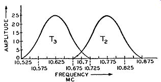
Fig. 7-23. Inasmuch as the two portions of the secondary of the discriminator
transformer are resonant at different frequencies, their response curves
are as shown at the right. Note that at only one frequency is the response
of both circuits the same.
Glancing again at Fig. 7-22, we see that each secondary tuned circuit is connected to a separate diode; both diodes may be contained either in a single envelope or in separate tubes. The method of connection of the load resistors across the output is such that the circuit is arranged in the form of a differential rectifier system. That is, the output voltages across the individual load resistors buck each other. If the individual diode current flow is traced, it will be evident that the top part of R1, at point A, is negative with respect to that part connected to the cathode of diode D1 and that the cathode connection of resistor R, to diode D, is positive with respect to ground. Consequently, these individual voltage drops across R1 and R2 or between point A and ground, oppose each other. The final rectified output voltage present across the series combination of load resistances, or between ground and point A, depends upon the relative magnitudes of the individual voltages across R1 and R2. If the two rectified voltages across R1 and R2 are equal, the net voltage between ground and point A is zero. If that across R2 is not equal to that across R 1, the final voltage between ground and point A is equal to the differences of the voltages. The polarity of the voltage between ground and point A is the same as the polarity of the greater of the individual voltages across R1 and R2. The negative signs of point A and ground voltage do not mean fixed polarity. These signs are used to indicate that the two load resistances are connected into a differential circuit and that the voltages across them tend to buck each other. Either point A or ground can be positive or negative with respect to the other, depending upon the magnitudes of the voltages across R1 and R8.
The significant detail is that at any one instant, only one frequency exists in the system, and whether D1, or D2, or both, rectify the signal depends entirely upon the frequency of the signal voltage. Thus, if at any one instant the frequency of the signal is 10.625 mhz, the circuit which responds to this frequency is T3 (see Fig. 7-23), and rectification will take place in D2 with the rectified voltage appearing across R2. As a matter of fact, this is true for all frequencies from 10.525 mhz to approximately 10.675 mhz. Between 10.675 mhz and 10.725 mhz, both tubes are operative, and the differential voltage is developed between point A and ground. Between 10.725 mhz and 10.875 mhz only T2 is responsive, and the signal is rectified in D1 with the rectified voltage appearing across R1. Recalling that the polarities of the voltages developed across R1 and R2 differ with respect to ground, we then have a situation wherein voltages positive with respect to ground, which can be the zero reference point, are developed across R2, and voltages negative with respect to ground are developed across R1. If we plot the output voltage developed across R1 and R2 respectively with respect to frequency, we secure a graph as in Fig. 7-24 (A). The response of the T., system is shown above the frequency reference line, because the voltage developed across R2 is positive with respect to ground. The response of the T2 system is below the reference line, because the voltage developed across R1 is negative with respect to ground.
These two curves are representative of the voltages existing between point A and ground in Fig. 7-22, and, consequently, they can be combined to form a resultant over-all curve. By doing this to the curves of Fig. 7-24 (A) we obtain a resultant curve which is the typical S characteristic of a discriminator, as shown in Fig. 7-24 (B). For example, at the mean frequency of 10.7 mhz the response of T 2 is the same as that of T 3, and the voltage developed across R1 is the same as that across R,; but, since they are of opposite polarity, they cancel, and the net output voltage from the rectifier system is zero as indicated.

Fig. 7-24 (A), left, (B) right. If the output voltage developed across
R1 and R2 of Fig. 7-22 is plotted against frequency, the response curves
of (A) are derived. These curves can be combined, as in (B), resulting
in the S characteristic of a discriminator.
Other output points are developed in similar fashion. For example, at 10.69 mhz greatest response is secured in T3 and according to Fig. 7-24 (A), the rectified voltage across R, is 6 volts, whereas the rectified voltage developed across R1 is 1 volt. Since these two voltages are of opposite polarity, the net final output voltage is 5 volts as shown in Fig. 7-24 (B), and the polarity of this voltage is positive with respect to ground, because the greater response to this frequency takes place across T3. Hence the greatest rectified voltage is developed in the T 3-D2 -R2 system.
Looking at Fig. 7-22 and Fig. 7-24 (B), we can make certain observations which will be of interest later. Here is a rectifying means whereby we can convert frequency variations into audio voltages of different amplitudes. Secondly, we see a zone of operation wherein a uniform change in frequency results in a linear output; this is over the straight portion of the curve between X and Y. Thirdly, we realize that to secure a linear output the frequency excursions should not exceed the linear portion of the discriminator characteristic. These curves are used only for illustrative purposes and do not typify circuits used in present-day receivers in which the linear portion of the tubes is 75 khz or greater.

Fig. 7-25. The action of the double tuned discriminator circuit of Fig.
7-22 in converting the frequency variations of the signal shown at the
lower left into a corresponding a-f signal of varying amplitude at the
upper right.
It might be well at this time to assume a signal of constant amplitude across the primary of a double tuned discriminator transformer, and to establish the manner in which the discriminator action produces the variable amplitude audio output. This is indicated in Fig. 7-25, wherein the operation of the circuit is assumed to be over the linear portion of the discriminator characteristic curve, which in this example is about 50 khz on either side of the center frequency. In Fig. 7-25, we have a wave indicating the frequency shift of the incoming i-f signal. This wave at the lower left side of the drawing is not an i-f signal as pictured in other parts of the text. The true input i-f signal to the discriminator is constant in amplitude but varying in frequency. To show these frequency changes in the FM signal, an other wave is plotted which indicates the changes in frequency. The variation in amplitude of this new wave indicates the changes in frequency at different instances of time.
Suppose that we apply to the discriminator tube an FM signal of i.f. constant in amplitude with a maximum deviation of 50 khz each side of 10.7 mhz, which is considered the center frequency of the signal.
Following the plotted points in Fig. 7-25, you will note that the output voltage from the discriminator is zero when the input signal is of the same frequency as the mean of the complete range covered by the discriminator response, namely 10.7 mhz. The reason for this was explained in connection with Figs. 7-23 and 7-24 (A) and (B). With the frequency of the input signal changing, we note that the first deviation is in the positive direction, that is the frequency increases to an extent indicated by A, and, at its maximum, the increase is equal to 25 khz. Since the design of the discriminator is such that when the frequency increases a negative voltage is developed in the output, we have, therefore, a change in output voltage from zero to minus 10 volts. If we show this output voltage with respect to a zero voltage reference line, we reach the peak negative voltage A' in the audio output curve. From A in the input signal curve, the frequency deviation decreases, and there is a corresponding decrease in the output voltage. Since the change in frequency is still within the plus zone, the output voltage is still negative until it reaches zero. The frequency of the input signal continues to change, but this time in the downward direction, and the design of the discriminator is such that when the frequency of the input signal is less than the center frequency, the output voltage is of positive polarity, and for the maximum frequency deviation of 25 khz in the downward direction indicated as B, the peak audio voltage is developed in the positive direction as indicated at B'. At this point the deviation in frequency of the input signal starts to decrease, and the audio output likewise decreases; but the deviation is still such that the frequency is less than the mean, so that the audio output voltage is still positive in polarity and, therefore, is shown above the zero reference line. When the frequency deviation of the input signal again is zero, the audio output voltage also becomes zero, and a complete audio cycle has been completed. This cycle of audio voltage is identified simply for the sake of illustration as 0.001 second, meaning that it is a single cycle of a 1000-cycle note.
The second audio cycle, which has been chosen at a higher audio frequency, is plotted by following the frequency deviation curve of the input carrier; at C it represents a deviation of 40 khz in the upward direction, and a negative voltage of slightly less than 18 volts is produced as shown at C'. In the downward direction the frequency deviation likewise is 40 khz, and the peak is shown at D. The equivalent point along the discriminator curve establishes the output voltage peak D'. The remaining cycles of the output are developed in the same manner.
Abandoning the double tuned discriminator shown in Fig. 7-22 for the present, we next discuss the center-tapped secondary type of discriminator actually employed in commercial circuits. Strange as it may seem, considering the foregoing lengthy discussion, the double tuned type is not in actual commercial use. It is more difficult to align, and the transformers are more critical in design than those used in the center-tapped discriminator. However, the operation of the diodes, including the audio voltage developed across the load resistance and the S characteristic of the discriminator, is the same for the double tuned circuit and the center-tapped types, so that the discussion of Figs. 7-24 (B) and 7-25 can be applied to the commercial variety of discriminators. In fact, discussion of some of the general details of interest associated with Fig. 7-25 has been reserved until after the operation of the center-tapped transformer discriminator and wherein it differs from the double-tuned circuit has been explained. It will be seen that the difference between the two is essentially in the tuned circuit arrangement.