Basically, an fm-stereo signal consists of two different audio-frequency signals that occupy the same fm channel. These separate audio signals provide stereophonic sound reproduction. The individual audio signals are identified as "left" (L) and "right" (R). In conventional programming, this pair of audio signals originates from a pair of microphones at a sound studio, as shown in Fig. 3-1. The audio signal from the L microphone differs from that of the R microphone. Therefore, the stereo signal consists of two audio waveforms that vary independently in frequency and amplitude. At the receiver, the Land R signals are fed to separate speakers. These speakers are spaced a suitable distance apart to simulate the placement of the transmitting microphones. Fig. 3-2 shows a block diagram of a typical am/fm stereo chassis. The multiplex section in this example comprises the bandpass amplifier, 19-kHz pilot amplifier, 38-kHz oscillator, stereo indicator, detector, and matrix sections.
Common trouble symptoms caused by defects in the multiplex sections are:
1. No output.
2. One channel dead.
3. Weak output.
4. Poor separation.
5. Distorted output.
6. Separation-control setting drifts.
7. Stereo indicator failure.
GENERAL DISCUSSION
We know that in monophonic fm transmission, a swing of ±75 kHz represents full modulation and produces sidebands that occupy the entire channel. For this reason, the question arises how one channel can be used to transmit two signals without mutual interference. If high fidelity were not required, an fm channel could be divided into two equal parts for transmission of the L and R signals on individual carriers. However, since hi-fi transmission is a basic requirement, a modulation method must be employed that permits each signal to occupy the entire channel bandwidth.
To transmit both the L and R signals with high fidelity in a single channel requires multiplex trans mission. This is a technique that permits satisfactory separation of the L and R signals at the receiver.
Standard multiplex transmissions are also compatible, which means that to a conventional mono receiver, the fm multiplex signal "looks like" a mono transmission. But to a stereo-multiplex receiver, the fm multiplex signal "looks like" separate L and R signals. A stereo-multiplex system starts with the conventional mono audio signal, which is produced as the sum of L and R signals. That is, two micro phones are employed as the equivalent of a single microphone. When the L and R signals are mixed, as shown in Fig. 3-3, the mono (L + R) signal is produced.
The L + R signal is frequency modulated on the RF carrier, and the result is the same as if a single microphone were used. Furthermore, to an ordinary fm receiver, only a mono signal is being transmitted--actually, as explained next, additional information to which an ordinary fm receiver is unresponsive is also being transmitted. To explain this additional transmitted information, let us consider the effect of adding a 38-kHz carrier as shown in Fig. 3-4. Both the L + R signal and the 38-kHz carrier are frequency-modulated on the RF carrier. However, only the L + R signal can be reproduced at the fm receiver. That is, the 38-kHz carrier is out of the range of audibility. This is the fundamental multiplex transmitting principle.

Fig. 3-1. Basic principle of stereophonic sound reproduction.

Fig. 3-2. Block diagram of a typical am/fm stereo chassis.

Fig. 3-3. Mixing of L and R signals produces a conventional monaural signal.

Fig. 3-4. L + R and 38-kHz signals modulated on an RF carrier. (A) Block
diagram. (B) Transmitted frequency spectrum.
Next, if amplitude modulation is impressed on the 38-kHz carrier, this modulated signal will be inaudible on an ordinary fm receiver. With reference to Fig. 3-5, the L + R signal is frequency-modulated on the RF carrier, as before. In addition, an audio signal, A2, is amplitude-modulated on the 38-kHz carrier; this amplitude modulation produces sidebands, and the RF carrier is modulated by these sidebands along with the L + R signal. Fig. 3-5B shows the frequency spectrum of the modulating waveforms. The L + R signal has frequencies up to 15 kHz. On the other hand, the amplitude-modulated 38-kHz carrier has frequencies in the range from 23 kHz to 53 kHz. This represents an audio-frequency range up to 15 kHz.
Note that after the foregoing frequency spectrum is frequency-modulated on the RF carrier and then processed through the ratio detector of an ordinary fm receiver, the frequency spectrum is recovered in its original form, as shown in Fig. 3-5B. Of course, only the L + R signal is reproduced by an ordinary fm receiver. In other words, the frequencies from 23 kHz to 53 kHz will be rejected by the audio system in an ordinary fm receiver; even if an extended range audio amplifier were used, the reproduced tones would be inaudible to the ear. In multiplex terminology the frequencies from 23 kHz to 53 kHz are said to be "encoded" in the radiated fm signal.
Now, let us see how the encoded signal is recovered. Fig. 3-6A shows a bandpass filter with response from 23 kHz to 53 kHz, driven by the ratio detector, and followed by an AM detector and a speaker. The bandpass filter picks out the AM signal, which is then demodulated by the AM detector. In turn, the demodulated (audio-frequency) wave envelope is fed to a speaker. This is the A2 signal shown in Fig. 3-5. Note that the output from the ratio detector in Fig. 3-6B is a mixture of the L + R and the A2 AM signal. Thus, the bandpass filter provides separation of the signals in this example. These basic functions are elaborated somewhat in actual practice so that the L signal will be reproduced by one speaker, and the R signal reproduced by another speaker. Basically, an L - R signal is generated by means of a phase inverter at the transmitter, as shown in Fig. 3-7.

Fig. 3-5. Amplitude-modulated 38-kHz subcarrier combined with L and R signals.

Fig. 3-6. Method for reproducing the multiplexed signal.
Observe that by inverting the polarity of the R signal and then adding it to the L signal, we obtain an L - R signal. In turn, both L +R and L - R signals are available for processing. If we add L + R to L - R, we will obtain 2L (the L signal with the R signal cancelled or separated). Again, if we sub tract L - R from L + R, we will obtain 2R (the R signal with the L signal cancelled or separated). Signal addition or subtraction is accomplished in mixers, with associated inverters. After the L and R signals have been separated from the L + R and L - R signals, we can feed the R signal to one speaker, and feed the L signal to the other speaker, thus obtaining stereo reproduction.
At the transmitter, the L + R and L - R signals are employed to frequency-modulate the RF carrier, as shown in Fig. 3-8. The L - R signal is amplitude modulated on a 38-kHz carrier, and the resulting signal is mixed with the L + R signal. In turn, the mixed signals frequency-modulate the RF carrier. Fig. 3-SB shows the frequency spectrum of the modulating signal, wherein the upper and lower sidebands flanking the 38-kHz carrier are produced by the L - R signal. At the receiver, this same frequency spectrum appears at the output of the ratio detector.
To obtain stereo reproduction, the L - R signal is separated by means of a 23- to 53-kHz bandpass filter, amplitude-demodulated, and further processed in a phase inverter and a pair of mixers, as shown in Fig. 3-9. The addition of L + R and L - R produces a 2L signal. Subtraction of L - R from L + R (the same as adding L + R and - L + R) produces a 2R signal. Thereby, stereo reproduction is obtained from the speakers. Hi-fi reproduction results if this processing is normal.
In theory, the 38-kHz carrier (technically termed the subcarrier) could be transmitted. However, the subcarrier is suppressed in practice, thereby permitting the L - R sidebands to be transmitted at a higher level, which improves the signal-to-noise ratio. In turn, the 38-kHz subcarrier must be reinserted at the receiver. This is accomplished by mixing a locally generated subcarrier with the L - R sidebands. This mixing process must be done at exactly the correct frequency and the exactly correct phase, in order to provide hi-fi reproduction. To permit precise reinsertion of the missing subcarrier at the receiver, a 19-kHz pilot subcarrier is transmitted.
Fig. 3-10 shows how the 19-kHz pilot subcarrier is transmitted in an empty portion of the spectrum be tween the L + R signal and the lower sideband of the L - R signal.

Fig. 3-7. Developing the L + R and L - R signals.

Fig. 3-8. Generation of the composite stereo signal at the transmitter.

Fig. 3-9. Block diagram of multiplex adapter for stereo reproduction.

Fig. 3-10. Composite stereo signal showing 19-kHz pilot sub-carrier in
empty portion of spectrum.
The pilot subcarrier is transmitted at relatively low power, and because it is separated from the L + R and L - R signals, it can be easily trapped at the receiver free from interference. Thus, both a 38 kHz and the related 19-kHz subcarrier are generated at the transmitter, but the 38-kHz subcarrier is trapped out prior to transmission, so that the L - R signal is radiated as a suppressed-carrier signal. At the receiver, a tuned trap picks out the pilot sub-carrier and feeds it to a doubler, thereby developing the missing 38-kHz subcarrier. This 38-kHz subcarrier is then mixed with the L - R sidebands, and the end result is the same as if the complete L - R signal had been transmitted.
Stereo-Multiplex Generators
Stereo-multiplex troubleshooting requires the use of a suitable generator. A basic generator supplies an L + R signal, an L - R signal, and a 19-kHz pilot subcarrier. The L + R and L - R signals have a 1-kHz audio frequency in the basic generator; the more elaborate generators may also provide 400-Hz and 5-kHz tones. Most generators include a 100-MHz RF oscillator, which may be frequency-modulated by the composite audio signal (Fig. 3-11). The composite audio signal is fed directly into a multiplex adapter (or combo section) for tests. On the other hand, an fm RF signal is required when the tests or measurements are made through the RF tuner. We will find that an L + R signal or an L - R signal seem to have the same waveform; this is because the only difference between them is their phase with respect to the pilot subcarrier. Let us see how these waveforms are produced by the generator.

Fig. 3-11. Checking the output from a multiplex generator. (A) Test setup.
(B) Normal 1-kHz composite audio signal. (C) Normal composite signal with
19-kHz pilot subcarrier.

Fig. 3-12. Development of the composite audio signal. SINE-WAVE SIGNAL
PLUS UPPER AND LOWER SIDEBANDS
With reference to Fig. 3-12, we observe:
1. The waveshape of the subcarrier and both side bands is the same as that of an ordinary amplitude-modulated signal.
2. When the subcarrier is suppressed, the side bands without the subcarrier form an envelope that has twice the frequency of the original envelope.
3. In the generator, an L + R (or L - R) signal is produced by modulating a 38-kHz sine wave by a 1-kHz sine wave, and then suppressing (removing) the 38-kHz frequency.
4. Next, to develop an R signal, we may consider the result of energizing the R microphone only in Fig. 3-7. In turn, with reference to Fig. 3-12, we see that the R sine-wave signal is mixed with the -R signal which consists of sidebands without subcarrier. This mixture produces the sine-wave signal plus upper and lower side bands.
5. If an L signal is to be developed, the end result is the same, except for a phase difference, since the output from the L microphone in Fig. 3-7 does not pass through a phase inverter.
In a stereo-multiplex generator, of course, the L and R signals are produced by audio oscillators in stead of microphones. The most basic test of a multiplex adapter is its ability to separate L + R and L - R signals. Fig. 3-13 shows a typical test setup.

Fig. 3-13. Setup for testing separation in a stereo system.
If a multiplex adapter is being checked without the fm tuner, we apply the composite audio signal to the adapter input terminals. Either a scope or an ac VTVM can be used as an indicator. In theory, when we apply an R-channel signal to the adapter, we would observe full output from the R section and zero output from the L section, as shown in Fig. 3-14A and B. In practice, however, separation can not be perfect, and the L channel output (undesired output) might appear as seen in Fig. 3-14C. Similarly, when an L-channel signal is applied to the adapter, it is impractical to reduce the undesired output from the R channel to zero.
A stereo-multiplex generator provides a test signal that has virtually complete separation, unless a defect occurs in the generator. In turn, we are concerned with how many decibels of separation should be normally provided by a multiplex adapter. A high-quality multiplex adapter ( or multiplex section in a combo) will provide approximately 30dB of separation. It is generally considered that a separation of 10 dB is barely tolerable. Note that 30 dB corresponds to a voltage ratio of more than 30 be tween the L and R channels. On the other hand, 10 dB corresponds to a voltage ratio of approximately 3 between the L and R channels. In the ex ample of Fig. 3-14, we have a voltage ratio of 7 to 1 between (a) and (c); this is equal to about 17 dB, and represents average multiplex-adapter performance. A VTVM with a dB scale is illustrated in Fig. 3-15; this provides convenience in making separation tests. Note that a multiplex adapter or section is basically a signal processor and provides practically no gain from input to output.

Fig. 3-14. Waveforms observed during separation test. (A) R-channel output.
(B) Ideal L-channel output.
(C) Normal L-channel output.
Defects That Cause Poor Separation
Although poor separation is usually caused by a component defect, drift in tuned-circuit adjustments can also impair separation. Four tuned circuits are utilized in a typical multiplex adapter, as shown in Fig. 3-16; the corresponding circuit is seen in Fig. 3-17. The composite stereo signal is amplified by V1A and then fed to the grid of phase-inverter V2A. V2B operates as a mixer for the two outputs from V2A after sampling by the ring demodulator consisting of X3 through X6. Always check tubes first. If V2 is not defective, check the other tubes also.
Next to tubes, capacitors are prime suspects. A systematic approach in this sample entails checking C8, C11, C9, C10, and C15. Courtesy EICO Electronic Instrument Co., Inc.

Fig. 3-15. VTVM with a dB scale.

Fig. 3-16. Markers show tuned-circuit locations in a typical multiplex
adapter.
In the event that no capacitor defects are found, the next step is to check ( or replace) the diodes in the ring demodulator. Diodes X3, X4, X5, and X6 must have good front-to-back ratios, and must also be reasonably well matched to obtain optimum separation. Another possibility of poor separation is a faulty frequency-doubling diode, such as X1 or X2; these diodes change the 19-kHz pilot subcarrier into a 38-kHz subcarrier. Resistors are less common troublemakers, but become ready suspects in case a shorted tube has been replaced. For example, R33 and R34 can be damaged by overloads. If R34 is in creased in value, V2B becomes incorrectly biased and does not operate as a linear mixer; in turn, separation is impaired. The setting of R31 determines the amount of L .LR signal that is applied to mixer V2B, and thereby affects separation. In case R31 checks out satisfactorily, we would check R35 as a possible troublemaker.
Alignment of a multiplex adapter or section is checked last, because this is statistically the least likely cause of poor separation (unless a do-it-your selfer has been tampering with the alignment adjustments). Alignment of the adapter in Fig. 3-17 is comparatively simple; T2 and T4 are the most critical circuits, and are peaked at 19 kHz and 38 kHz, respectively. To align T2, we inject an unmodulated 19-kHz signal at the grid of V1, and connect an ac VTVM at the plate of V4. The slug in T2 is then adjusted for maximum output. To align T3, inject a 19-kHz signal at the grid of V 4 and connect an ac VTVM at the plate of V5A. The slug in T3 is then adjusted for maximum output. To align T4, we inject a 38-kHz signal at the grid of V5A, and connect an ac VTVM at the junction of X5 and X6. Then, the slug in T4 is adjusted for maximum output. Some times a slight compromise adjustment of T4 will give optimum separation.
Note that T5 in Fig. 3-17 is a 67-kHz trap. It is tuned by a slug (not shown in the diagram). This circuit does not affect separation; instead, its purpose is to suppress "birdies" in case an SCA signal is being transmitted. With reference to Fig. 3-18, an SCA signal employs a 67-kHz subcarrier. A subsidiary-carrier-assignment (SCA or store-casting) signal cannot be heard on a conventional stereo multiplex receiver, unless a special SCA adapter is used. However, an SCA signal can sometimes cause "birdies" in conventional fm stereo reception unless the SCA signal is trapped out. To check the alignment of T5 in Fig. 3-17, we feed a 67-kHz signal into the adapter, and connect an ac VTVM at the plate of V1A. Then, the slug in T5 is adjusted for minimum output.

Fig. 3-17

Fig. 3-18. Frequency spectrum of signals applied to modulator in fm transmitter.
(A) Right microphone energized; composite signal at receiver with subcarrier inserted.
(B) Both microphones energized; composite signal at receiver with subcarrier inserted.

Fig. 3-19. Representative multiplex waveforms.
Although the end result is the same, the configuration in Fig. 3-17 processes the multiplex waveform in a different manner from the arrangement in Fig. 3-9.
That is, the multiplex signal is sampled in Fig. 3-17.
It is important that this process be understood. The waveforms shown in Fig. 3-19 show how the envelopes above and below the zero axis provide the L and R signals after the 38-kHz subcarrier is inserted. Thus, the positive and negative excursions of the subcarrier serve to develop the individual L and R signals in the bridge circuit of Fig. 3-17. We will find another processing method called the envelope-detector configuration; this method employs a pair of oppositely polarized amplitude detectors.
It is evident that when a multiplex waveform passes through a positively polarized detector, the output waveform will be the R signal. Similarly, the out put from a negatively polarized detector will be the L signal.
Stereo-Indicator Circuits
Most receivers have lamps that indicate when a stereo broadcast signal is being received. Typical arrangements are shown in Figs. 3-20 and 3-21. The first section, in Fig. 3-20A, is actuated by the pilot- amplifier signal. The input circuit couples 19-kHz energy to the lamp-amplifier stage, whenever a pilot carrier is present. This amplifier is a conventional emitter follower. The output load of the control transistor is a relay coil, which is returned to the collector-supply voltage. When a drive signal is applied, the bias on the control transistor changes, and the collector current increases. In turn, the relay closes and a potential of 12 volts is applied to the indicator lamp.
Next, with reference to Fig. 3-20B, the three stages operate as DC amplifiers. Actuating energy is obtained from the pilot oscillator. In turn, the 38-kHz signal is rectified by twin diodes X14 and X15, which operate in the sensing stage. The negative-going change in DC voltage at the base of Q11 produces an opposite change at its collector. Thus, the base of Q12, connected directly to the Q11 collector, is driven positive. In turn, the voltages at the collector of Q12 and the base of Q13 go negative. This voltage change causes Q13 to conduct heavily. Since there is collector current through the stereo-indicator lamps, their filaments glow as long as the base of Q13 remains negative. Note that the input circuit for Q11 is a filter that smooths the pulsating outputs from the input diodes. Additional filtering is provided by C121.
The stereo-indicator arrangements in Fig. 3-21 are comparatively simple. Both of them operate by means of applied DC voltages at the bases of the transistors. In Fig. 3-21A the pulsating-de output from the pilot-subcarrier doubler circuit is filtered by means of a 5-µF capacitor, and drives the base positive, thereby turning the transistor on. The arrangement in Fig. 3-21B is basically similar, except that two stages are provided. Note also that the input is actuated by the output from a balanced stereo detector; therefore, less filtering is required at the base of the input transistor.

Fig. 3-20. Stereo-indicator light circuits. (A) Actuated by pilot-amplifier
signals. (B) Actuated by pilot oscillator.
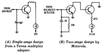
Fig. 3-21. Two simple stereo-light systems. (A) Single-stage design from
a Tenna multiplex adapter. (B) Two-stage design by Motorola.
TROUBLESHOOTING PROCEDURE
Bench work on an operating complaint starts with localization of the defective section. With reference to Fig. 3-2, trouble in the bandpass or matrix section could be confused with trouble in the ratio-detector circuit, or with a defect in one of the audio channels.
Therefore, it is advisable to drive the multiplex section directly with the audio composite signal from a multiplex generator. For example, the signal would be applied at Ml in Fig. 3-17. A scope can be connected at M2 for preliminary analysis of the Ch-1 output; next, the scope can be connected at M3 for analysis of the Ch-2 output. This approach will identify prominent malfunctions, such as lack of output on one or both channels, poor separation, high hum level, or serious waveform distortion.
On the other hand, less prominent malfunctions such as moderate distortion or poor frequency response require additional tests for definite identification. A harmonic-distortion meter must be connected in place of the scope at the output of the multiplex adapter to measure percentage of distortion. Fig. 3-22 shows the test setup that is used. If it is suspected that the adapter has poor frequency response, the multiplex generator is externally modulated by means of an audio oscillator, and the output from the adapter is indicated by an ac VTVM as shown in Fig. 3-23. The adapter should provide a reasonably flat frequency response from 20 Hz to 15 kHz, prior to the de-emphasis network.

Fig. 3-22. Harmonic-distortion test setup for a multiplex adapter.

Fig. 3-23. Frequency-response check of a multiplex adapter.
In the case of a "dead" adapter, or lack of output on one channel, conventional signal-tracing procedures with a scope are useful to localize the defective stage or circuit section. Then, DC voltage and/or resistance measurements will usually serve to close in on the defective component. Most operating troubles in multiplex adapters are caused by leaky or open capacitors. However, a worn and erratic separation control occasionally causes trouble, and may be over looked by the technician apprentice. Some adapters are designed to operate with a certain value of input cable capacitance; if a cable with excessive capacitance is substituted, trouble symptoms may be introduced. Note also in Fig. 3-17 that C25 operates in combination with T5 to produce optimum SCA rejection. However, when using some types of fm tuners, C25 may affect the range of the separation control; that is, the separation control might require setting near one end or the other, or might be out of range. In such a case, we vary the value of C25 from 2700 pF to zero, choosing the value that provides midrange setting of the separation control.
Finally, T5 should be realigned for optimum 67-kHz rejection.

Fig. 3-25. Markers show tuned-circuit locations in a transistor multiplex
adapter.

Fig. 3-24. A. transistor multiplex adapter.
The troubleshooting procedure for a transistor multiplex unit is much the same as for a tube-type unit, since designs are based on a transistor-for-tube basis, as seen in Fig. 3-24. A typical adapter is illustrated in Fig. 3-25. With reference to Fig. 3-24, Q1 is a high-impedance input transistor, with a 19-kHz resonant trap in its emitter circuit. Thus, the 19-kHz pilot subcarrier is dropped across the trap, and does not appear in the collector circuit. SCA signals are rejected by T1. Q2 operates as an emitter-follower buffer stage for the multiplex signal. Q3 amplifies the 19-kHz pilot subcarrier, and Q4 operates as a 38-kHz locked oscillator, synchronized by the out put from Q3. In turn, the complete multiplex signal appears at the secondary of T4. Diodes X1 through X4 operate in a switching bridge; X1 and X4 provide the R signal output, while X2 and X3 provide the L signal output. Note that the de-emphasis networks comprise series 150-k resistors with 0.001-µF shunt capacitors.
In normal operation, we will find a separation of approximately 25 dB between the L and R channels.
An input signal level of at least 0.5 volt rms is required to maintain tight locking of the 38-kHz sub carrier oscillator. At lower values of input signal, the oscillator locks erratically, causing serious distortion and noise in the output. This is a comparatively simple design, which does not employ a stereo-indicator light. We will find that there is a small amount of 19-kHz and 38-kHz signal in the L and R outputs; the normal 19-kHz rejection is greater than 20 dB, and the 38-kHz rejection is greater than 30 dB below 1 volt. To obtain an accurate harmonic distortion test, the 19- and 38-kHz residual signals can be effectively suppressed by passing the adapter output through a 15-kHz audio amplifier.
By way of comparison, we will observe in Fig. 3-17 that all residual signals above 15 kHz are greatly attenuated by means of pi filters inserted in the L and R output circuits. One of these pi filters comprises L1, C18, C21, and C17; the other filter comprises L2, C19, C22, and C20. Basically, filtering is not provided for convenience of testing, but to avoid interference in tape-recording procedures. That is, tape recorders employ ultrasonic ac bias, which can form audible beats with ultrasonic residual signals that are produced in the multiplex decoding process.
By providing filter action, the residual signals are reduced to an imperceptible level.

Fig. 3-26. Block diagram for circuit of Fig. 3-24.
ANALYSIS OF COMMON SYMPTOMS
An analysis of the common trouble symptoms listed earlier in this Section is presented in this section.
1. No Output When there is no output from either the L or the R channel, we know that the defect is common to both channels. For example, there might be an interruption of supply voltage to the multiplex adapter.
Again, the input plug might not be fully inserted. In case the trouble is not readily apparent, it is helpful to analyze the circuit diagram of the unit, to determine the signal-flow paths. If we avoid a "shot gun" approach, we will usually save considerable time in the long run. After identifying the signal test points in the circuit, a scope can be used to trace up to the defective component or branch.
Possible causes of signal stoppage in a multiplex configuration are:
a. Open coupling capacitor to base of transistor, such as Q1 in Fig. 3-24.
b. Leaky or shorted capacitor, causing cutoff or saturation of transistor.
c. Transistor failure.
d. Cracked PC board, or damaged printed wiring.
e. Unsoldered or cold-soldered connection.
f. Defective transistor (not likely, but possible).
2. One Channel Dead
If only one channel is dead in a multiplex unit, the trouble symptom provides preliminary localization.
The signal-flow paths can be determined by analysis of the circuit diagram, and signal-tracing with a scope will lead to the defective branch circuit or component. For example, with reference to Fig. 3-24, a block diagram that denotes signal-flow paths can be drawn as exemplified in Fig. 3-26.
Possible defects causing one channel to fail are as follows:
a. Open capacitor, such as a series capacitor in output lead of a channel.
b. Shorted capacitor, such as a de-emphasis capacitor in output lead of a channel.
c. Cracked PC board, or damaged printed wiring.
d. Poor connection or otherwise open secondary winding in 38-kHz transformer (such as terminal 1 of T4 in Fig. 3-24).
e. Output connector not fully inserted.
3. Weak Output
A defect that causes weak output may affect one or both channels. In case both channels have sub normal output, we know that the defect is in a circuit that is common to both the L and R channels.
Normal waveform amplitudes are seldom specified in the service data. Therefore, it is helpful to compare the observed amplitudes with those in another adapter of the same type. When the defective circuit has been localized, DC voltage and resistance measurements will usually serve to pinpoint the defective component.
Possible defects that cause weak output on one or both channels are:
a. Leaky coupling capacitor.
b. Open bypass capacitor.
c. Transistor with collector leakage.
d. Off-value bias resistor (less likely, but possible).
e. Low Vee supply voltage.
f. Replacement transistor incorrectly wired into circuit.
4. Poor Separation
Poor separation can be caused either by component defects or by misalignment of a multiplex Stereo Multiplex Troubleshooting adapter. Alignment is particularly critical in the matrix-type decoder; with reference to Fig. 3-9, the bandpass has an optimum frequency response shown in Fig. 3-27. Although not shown, the bandpass circuit has a phase characteristic that affects the relative timing of the upper and lower sidebands in the L - R signal. In theory, the phase characteristic should be linear; however, in practice, linearity can only be approximated. A bandpass circuit has best linearity when the frequency characteristic has the shape shown in Fig. 3-27.
Possible defects that can cause poor separation are as follows:
a. Poor front-to-back ratios, or unmatched diodes in sampling bridge.
b. Leaky capacitor in sampling-bridge circuit.
c. Weak output from 38-kHz oscillator (check for transistor collector leakage) .
d. Misalignment of bandpass circuit.
e. Off-value resistor in matrix or bridge circuit (less likely, but possible).
5. Distorted Output
Two basic types of distortion can occur in multiplex adapters; these are nonlinear distortion and frequency distortion, as explained previously. Distortion can also be caused by interference, such as SCA squeals or birdies due to trap misalignment or defects. Erratic locking of the 38-kHz subcarrier oscillator can also cause distortion. For example, sub normal supply voltage can result in audio distortion.
Possible defects that can cause distorted output are as follows:
a. Leaky capacitor in sampling bridge.
b. Defective diode in sampling bridge.
c. Transistor with collector leakage.
d. Marginal electrolytic capacitor in subcarrier oscillator section.
e. Defective or mistuned SCA trap.
f. Off-value resistor (less likely than preceding defects).

Fig. 3-27. Response of bandpass filter.
6. Separation-Control Setting Drifts
When the separation-control setting drifts, there is an unstable component present that affects the separation process. Separation controls are provided only in matrix-type multiplex units; for example, a separation control (R31) is included in the con figuration of Fig. 3-17, whereas no separation control is present in Fig. 3-24. An elusive troublemaker consists of a worn and erratic separation control, be cause the possibility of resistance drift in this component is often overlooked. Therefore, we should always check the control first.
Possible defects that can cause the separation control setting to drift are as follows:
a. Deteriorating bypass capacitor.
b. Coupling capacitor with unstable leakage condition.
c. Marginal diode or transistor.
d. Poor connection with fluctuating contact resistance.
e. Inconstant supply voltage to adapter unit.
f. Burned or otherwise defective resistor.

Fig. 3-28. Poor connection to pin 9 on M4 caused failure of stereo indicator.
7. Stereo-Indicator
Failure In most cases, stereo-indicator failure is obvious, and requires only the replacement of a burned-out lamp. However, if the lamp is not burned out, broken, or otherwise defective, we turn our attention to the indicator circuit and its components. A stereo fm indicator bulb will light only if a stereo multiplex signal is applied to the adapter section. If the 19-kHz or 38-kHz tuned circuits are badly out of alignment for any reason, the stereo-indicator circuit cannot be energized. However, we check alignment last, unless there is reason to believe that the adjustments have been tampered with.
Possible defects that can cause stereo-indicator failure are as follows:
a. Defective switch contact, or poor connection. (See Fig. 3-28.)
b. Stereo-indicator light plug not fully inserted.
c. Open coupling capacitor, such as C91 in Fig. 3-20A.
d. Shorted capacitor, such as C121 in Fig. 3-20B.
e. Defective transistor in indicator section.
f. Diode with poor front-to-back ratio, such as X15 in Fig. 3-20B.