In principle, the function of an audio power amplifier is a simple one: to convert a low-power input voltage signal from a pre-amplifier or other signal source into a higher power signal capable of driving a loudspeaker or other output load, and to perform this amplification with the least possible alteration of the input waveform or to the gain/frequency or phase/frequency relationships of the input signal.
VALVE (VACUUM TUBE) AMPLIFIER DESIGNS
In the earlier days of audio amplifiers, this function was performed by a two- or three-valve (tube) circuit design employing a single output triode or pentode, transformer coupled to the load, and offering typical harmonic distortion levels, at full power -- which would be, perhaps, in the range 2-8 W -- of the order of 5-10% THD, at 1 kHz, and amplifier output stages of this kind formed the mainstay of radio receivers and radiograms in the period preceding and immediately following the Second World War.
With the improvement in the quality of phonograph recordings and radio broadcasts following the end of the war, and the development of the new 'beam tetrode' as a replacement for the output pentode valve, the simple 'single-ended' triode or pentode output stage was replaced by push-pull output stages. These used beam tetrodes either triode-connected, as in the celebrated Williamson design, or with a more complex output transformer design, as in the so-called Ultra-linear layout, or in the Quad design, shown in Figs 1(a), (b) and (c). The beam tetrode valve construction, largely the work of the Marconi Osram valve company of London, offered a considerable improvement in the distortion characteristics of the output pentode, while retaining the greater efficiency of that valve in comparison with the output triode. This advantage in efficiency was largely retained when the second grid was connected to the anode so that it operated as a triode.
This electrode interconnection was adopted in the Williamson design, shown in FIG. 2, in which a substantial amount of overall negative feedback was employed, to give a harmonic distortion figure of better than 0.1%, at the rated 15 W output power.

FIG. 1 Push-pull valve amplifier output stages. (a) Triode (b) 'Ultra-linear'
(c) 'Quad'.
In general, the principle quality determining factor of such an audio amplifier was the output transformer, which coupled the relatively high output impedance of the output valves to the low impedance of the loudspeaker load, and good performance demanded a carefully designed and made component for this position. Nevertheless, such valve amplifier designs did give an excellent audio performance, and even attract a nostalgic following to this day.

FIG. 2 The Williamson amplifier.
EARLY TRANSISTOR CIRCUITS
With the advent of semiconductors with significant power handling capacity, and the growing confidence of designers in their use, transistor audio amplifier designs began to emerge, largely based on the 'quasi complementary' output transistor configuration designed by HC Lin, which is shown in FIG. 3. This allowed the construction of a push-pull power output stage in which only PNP power transistors were employed, these being the only kind then available. It was intended basically for use with the earlier diffused junction Germanium transistors, with which it worked adequately well.
However, Germanium power transistors at that time had both a limited power capability and a questionable reliability, due to their intolerance of junction temperatures much in excess of 100° C. The availability of silicon power transistors, which did not suffer from this problem to such a marked degree, prompted the injudicious appearance of a crop of solid state audio amplifiers from manufacturers whose valve operated designs had enjoyed an erstwhile high reputation in this field.
LISTENER FATIGUE AND CROSSOVER DISTORTION
Fairly rapidly after these new semiconductor-based audio amplifiers were introduced, murmurings of discontent began to be heard from their users, who claimed, quite justifiably, that these amplifiers did not give the same warmth and fullness of tone as the previous valve designs, and the term 'listener fatigue' was coined to describe the user's reaction.
The problem, in this case, was a simple one. In all previous audio amplifier experience, it had been found to be sufficient to measure the distortion and other performance characteristics at full output power, since it could reasonably be assumed that the performance of the amplifier would improve as the power level was reduced. This was not true for these early transistor audio amplifiers, in which the performance at full power was probably the best it would ever give.
This circumstance arose because, although the power transistors were capable of increased thermal dissipation, it was still inadequate to allow the output devices to be operated in the 'Class A' mode, always employed in conventional valve operated power output stages, in which the quiescent operating current, under zero output power conditions, was the same as that at maximum output.

FIG. 3 Quasi-complementary push-pull transistor output stage from HC Lin.
Crossover problems
It was normal practice, therefore, with transistor designs, to bias the output devices into 'Class B' or ' Class AB', in which the quiescent current was either zero, or substantially less than that at full output power, in order to increase the operating efficiency, and lessen the thermal dissipation of the amplifier.
This led to the type of defect known as 'crossover distortion', which is an inherent problem in any class 'B' or ‘AB' output stage, and is conspicuous in silicon junction transistors, because of the abrupt turn-on of output current with increasing base voltage, of the form shown in FIG. 4.
In a push-pull output stage employing such devices, the transfer characteristics would be as shown in FIG. 5(b), rather than the ideal straight line transfer of FIG. 5(a). This problem is worsened anyway, in the quasi-complementary Lin design, because the slopes of the upper and lower transfer characteristics are different, as shown in FIG. 5(c). The resulting kink in the transfer characteristic shown in FIG. 5(d) lessens or removes the gain of the amplifier for low-level signals which cause only a limited excursion on either side of the zero voltage axis, and leads to a 'thin' sound from the amplifier.
It also leads to a distortion characteristic which is substantially worse at low power levels - at which much listening actually takes place - than at full power output. Moreover, the type of distortion products generated by crossover distortion comprise the dissonant seventh, ninth, eleventh and thirteenth harmonics, which are much more objectionable, audibly, than the second and third harmonics associated with the previous valve amplifier designs.

FIG. 4 Turn-on characteristics of silicon junction transistor.
Additionally, the absence of the output transformer from such transistor amplifier designs allowed the designers to employ much greater amounts of negative feedback (NFB) from the output to the input of the circuit, to attempt to remedy the non-linear transfer characteristics of the system.
This increased level of NFB impaired both the load stability and the transient response of the amplifier, which led to an 'edgy' sound. High levels of NFB also led to a more precise and rigid overload clipping level.
Such a proneness to 'hard' clipping also impaired the sound quality of the unit.
This failure on the part of the amplifier manufacturers to test their designs adequately before offering them for sale in what must be seen in retrospect as a headlong rush to offer new technology is to be deplored for several reasons.

FIG. 5 Transistor ' Class AB' push-pull output stage characteristics. (Line
'a' is a straight line for comparison.)
Of these, the first is that it saddled many unsuspecting members of the public with equipment which was unsatisfactory, or indeed unpleasant, in use. The second is that it tended to undermine the confidence of the lay user in the value of specifications - simply because the right tests were not made, and the correct parameters were left unspecified. Finally, it allowed a 'foot in the door' for those whose training was not in the field of engineering, and who believed that technology was too important to be left to the technologists.
The growth of this latter belief, with its emphasis on subjective assessments made by self-appointed pundits, has exerted a confusing influence on the whole field of audio engineering, it has led to irrationally based choices in consumer purchases and preferences, so that many of the developments in audio engineering over the past two decades, which have been substantial, have occurred in spite of, and frequently in the face of, well-publicized and hostile opposition from these critics.
IMPROVED TRANSISTOR AMPLIFIER DESIGNS
The two major developments which occurred in transistor output circuit technology, which allowed the design of transistor power amplifiers which had a low inherent level of crossover distortion, were the introduction in the mid 1960s of fully complementary (NPN and PNP) output power transistors by Motorola Semiconductors Inc, and the invention by IM Shaw (Wireless World, June 1969), subsequently refined by P. J. Baxandall (Wireless World, September 1969) of a simple circuit modification to the basic quasi-complementary output push-pull pair to increase its symmetry.
These layouts are shown in Figs 6(a) and (b). The modified version shown in FIG. 6(c) is that used by the author in his Hi-Fi News 75 W power amplifier design , for which the complete circuit is given in FIG.
In many ways the Shaw/Baxandall quasi-complementary output transistor circuit is preferable to the use of fully complementary output transistors, since, to quote J. Vereker of Naim Audio, NPN and PNP power transistors are only really as equivalent as a man and a woman of the same weight and height' - the problem being that the different distribution of the N- and P doped layers leads to significant differences in the HF performance of the devices. Thus, although the circuit may have a good symmetry at low frequencies, it becomes progressively less symmetrical with increasing operating frequency.
With modern transistor types, having a higher current gain transition frequency (that frequency at which the current gain decreases to unity), the HF symmetry of fully complementary output stages is improved, but it’s still less good than desired, so the relative frequency/phase characteristics of each half of the driver circuit may need to be adjusted to obtain optimum performance.


FIG. 6 Improved push-pull transistor output stages.

FIG. 7 JLH Hi-Fi News 75 W audio amplifier.

FIG. 8 Power MOSFET structure, (a) V-MOSFET, (b) U-MOSFET, (c) D-MOSFET.
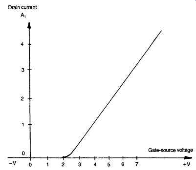
FIG. 9 Power MOSFET operating characteristics.
POWER MOSFETs
These transistor types, whose operation is based on the mobility of electrostatically induced charge layers (electrons or 'holes') through a very narrow layer of undoped or carrier-depleted silicon, have a greatly superior performance to that of bipolar junction transistors, both in respect of maximum operating frequency and linearity, and allow considerable improvements in power amplifier performance for any given degree of circuit complexity.
Two forms of construction are currently employed for power MOSFETs, the vertical or 'V MOSFET, which can employ either a 'V’ or a 'U' groove formation, of the types shown in Figs 8(a) and (b); though, of these two, the latter is preferred because of the lower electrostatic stress levels associated with its flat-bottomed groove formation; or the 'D' MOSFET shown in FIG. 8(c). These devices are typically of the 'enhancement' type, in which no current flows at zero gate/source voltage, but which begin to conduct, progressively, as the forward gate voltage is increased. Once the conduction region has been reached, the relationship between gate voltage and drain current is very linear, as shown.
By comparison with 'bipolar' junction power transistors, of conventional types, the MOSFET, which can be made in both N channel and P channel types to allow symmetrical circuit layout - though there is a more limited choice of P channel devices - does not suffer from stored charge effects which limit the 'turn-off speed of bipolar transistors.
The greater speed and lesser internal phase shifts of power amplifiers based on power MOSFETs allow greater freedom in the design of overall NFB layouts. This in turn, gives superior performance in the middle to upper frequency range. Greater care is needed, in the circuit design, however to avoid high frequency parasitic oscillation, which can cause rapid failure of the devices.
The principal technical problem in the evolution of power transistors derived from these charge operated devices, as distinct from the existing small signal MOSFETs, lies in obtaining an adequate capacity for current flow through the device. This problem is solved in two ways; by making the conduction path through which the current must flow as short as possible, and by fabricating a multiplicity of conducting elements on the surface of the silicon slice, which can be connected in parallel to lower the conducting resistance of the device.
V and U types
In the 'V’ or 'U' groove MOSFET, taking the case of the '?' channel devices shown in FIG. 8, the required narrow conduction channel, in which electrostatically formed negative charges (electrons) may be induced in the depleted T' type layer, is obtained by etching a channel through a previously diffused, or epitaxially grown, pair of differently doped layers.
With modern technology the effective thickness of such layers can be controlled with great precision.
In the case of the D-MOS device of FIG. 8(c), the required narrow channel length is achieved by the very precise geometry of the diffusion masks used to position the doped regions. It’s customary in the D-MOS devices to use a polycrystalline silicon conducting layer, rather than aluminum, to provide the gate electrode, since this offers a lower likelihood of contamination of the thin gate insulating layer.
In all of these MOS devices, the method of operation is that a voltage applied to the gate electrode will cause a charge to be induced in the semiconductor layer immediately below it, which, since this layer of charge is mobile, will cause the device to conduct.
Both for the 'V/U' MOS and the D' MOS devices, the voltage breakdown threshold of the gate insulating layer, which must be thin if the device is to operate at all, will be in the range 15-35 V. It can be seen that part of this gate insulating layer lies between the gate electrode and the relatively high voltage 'drain' electrode. Avoidance of gate/drain voltage breakdown depends therefore on there being an adequate voltage drop across the N-doped intervening drain region. This in turn depends on the total current flow through the device.
This has the effect that the actual gate/drain breakdown voltage is output current-dependent, and that some protective circuitry may need to be used, as in the case of bipolar output transistors, if damage is to be avoided.
OUTPUT TRANSISTOR PROTECTION
An inconvenient characteristic of all junction transistors is that the forward voltage of the P-N junction decreases as its temperature is increased. This leads to the problem that if the current through the device is high enough to cause significant heating of the base-emitter region, the forward voltage drop will decrease. If, due to fortuitous variations in the thickness of this layer or in its doping level, some regions of this junction area heat up more than others, then the forward voltage drop of these areas will be less, and current will tend to be funneled through these areas causing yet further heating.
This causes the problem known as 'thermal runaway' and the phenomenon of secondary breakdown, if certain products of operating current and voltage are exceeded. The permitted regions of operation for any particular bipolar transistor type will be specified by the manufacturers in a 'safe operating area' (SOA) curve, of the type shown in FIG. 10.
The circuit designer must take care that these safe operating conditions are not exceeded in use , for example by the inadvertent operation of the amplifier into a short-circuited output load. Provided that the SO A limits are not greatly exceeded, a simple fuse on the output circuit will probably be adequate, but a more effective type of protection is that given by the clamp transistors, Q7 and Q8 in the power amplifier design shown in FIG.
In this circuit arrangement, designed by A. R. Bailey, the clamp transistors monitor simultaneously the voltage present across the output transistors, by means , for example, of R18 and R23, and also the output current, in the case of the upper output transistor, by monitoring the voltage developed across R2ç. If the combination of these two voltage contributions exceeds the 0.55 V turn-on voltage of the clamp transistor, (Q7), it will conduct and shunt the input signal applied to the first transistor of the output pair (Q10) and avoid output transistor damage.

FIG. 10 Typical safe operating area (SOA) curve for junction power transistor.
In the case of power MOSFETs, a simple zener diode, connected to limit the maximum forward voltage which can be applied to the output device, may be quite adequate. An example of this type of output stage protection is shown in the circuit for the output stages of a 45 W power MOSFET amplifier designed by the author, shown in FIG. 11.

FIG. 11 Zener diode protection for power MOSFET output stage.
POWER OUTPUT AND POWER DISSIPATION
One of the most significant changes in audio technology during the past 30 years has been in the design of loudspeaker units, in which the electro acoustic efficiency, in terms of the output sound level for a given electrical power input, has been progressively traded off against flatness of frequency response and reduced coloration.
This is particularly notable in respect of the low-frequency extension of the LS response, in closed box 'infinite baffle' systems. Among other changes here, the use of more massive bass driver diaphragms to lower the fundamental resonant frequency of the system - below which a - 12 dB/octave fall-off in sound output will occur - requires that more input power is required to produce the same diaphragm acceleration.
On the credit side, the power handling capacity of modern LS systems has also been increased, so that equivalent or greater sound output levels are still obtainable, but at the cost of much greater input power levels.
Power levels
As a specific example of the power levels which may be needed for realistic reproduction of live sounds using typical modern LS units, recent measurements made in a recording studio showed that the peak output power required from the amplifier to match the peak sound levels produced by a grand piano played by a professional musician in the same room, was in excess of 300 W per channel. This test was made using a pair of high quality monitor speakers, of a kind also widely used in domestic hi-fi setups, whose overall efficiency was typical of modern designs.
No conventional valve amplifier, operating in 'Class A', could meet this power output requirement, in a stereo system, without the penalties incurred in terms of size, cost, and heat output being intolerable. In contrast the solid-state class AB power amplifier actually used in this test fitted comfortably into a 7 in. high slot in a standard 19 in. rack, and ran cool in use.
This reduction in LS efficiency has led to compensatory increases in power amplifier capability, so that the typical output power of a contemporary domestic audio amplifier will be in the range 50-100 W, measured usually with a 4 or 8 ohm resistive load, with 25 or 30 W units, which would at one time have been thought to be very high power units, now being restricted to budget priced 'mini' systems.
Design requirements
The design requirements for such power output levels may be seen by considering the case of a 100 W power amplifier using junction transistors in an output stage circuit of the form shown in FIG. 12, the current demand is given by the formula.
/ = ?/PÎR
where P = 100, and R = 8.
This gives an output current value of 3.53 A (RMS), equivalent to a peak current of 5 A for each half cycle of a sinusoidal output signal. At this current the required base-emitter potential for Q3 will be about 3 V, and allowing for the collector-emitter voltage drop of Q1? the expected emitter-collector voltage in Q3 will be of the order of 5V.

FIG. 12 Typical transistor output stage.
In an 8 ohm load, a peak current of 5 A will lead to a peak voltage, in each half cycle, of 40 V. Adding the 1.1 V drop across R3, it can be seen that the minimum supply voltage for the positive line supply must be at least 46.1 V. Since the circuit is symmetrical, the same calculations will apply to the potential of the negative supply line. However, in any practical design, the supply voltages chosen will be somewhat greater than the calculated minimum, so line voltages of ±50 V would probably be used.
For a true 'Class A' system, in which both of the output transistors remained in conduction for the whole output cycle, an operating current of at least 5 A, DC, would be required, leading to an output stage dissipation , for each channel, of 500 W. In the case of a typical ' Class AB' output stage, with a quiescent current of 100 mA, a much more modest no-signal dissipation of 10 W would be required. At full power, the device dissipation may be calculated from the consideration that the RMS current into the load, in each half cycle, will be 3.53 A giving an RMS voltage swing of 28.24 V. The mean voltage across each device during the half cycle of its conduction would therefore be 50 minus 28.24, and the mean dissipation , for each half of the power output stage would be 76.8 W. The worst case dissipation for such output stages, depending on supply line voltage margins, will be at about half power, where the dissipation in each half of the output stage could rise to 80-85 W, and the heat sinking arrangements provided must be adequate to meet this need. It’s still, however, only a third of that required by a 'Class A' system, and even then only required on power peaks, which, with typical program material, occur infrequently so that the average output stage heat dissipation, even under conditions where the amplifier is used at near its rated maximum power output, may well only be 20-30 W.
GENERAL DESIGN CONSIDERATIONS
Some of the techniques used for obtaining high gain and good linearity from a voltage amplifier stage, using semiconductors, were discussed in SECTION 4. However, in the case of low-power voltage amplifier stages, all of the gain elements will be operated in 'Class A', so that there won’t be a need to employ large amounts of overall negative feedback (NFB) to assist in linearizing the operating characteristics of the stage.
In power amplifier circuits, on the other hand, the output devices will almost certainly be operated in a non-linear part of their characteristics, where a higher level of NFB will be needed to reduce the associated distortion components to an acceptable level.
Other approaches have been adopted in the case of power amplifier circuits, such as the feed-forward of the error signal, or the division of the output stage into low power 'Class A' and high power 'Class B' sections.
These techniques will be discussed later. Nevertheless, even in these more sophisticated designs, overall NFB will still be employed, and the problems inherent in its use must be solved if a satisfactory performance is to be obtained.
Of these problems, the first and most immediate is that of feedback loop stability. The Nyquist criterion for stability in any system employing negative feedback is that, allowing for any attenuation in the feedback path, the loop gain of the system must be less than unity at any frequency at which the loop phase shift reaches 180°.
Bode Plot
This requirement is most easily shown in the 'Bode Plot' of gain versus frequency illustrated in FIG. 13. In the case of a direct-coupled amplifier circuit, and most modern transistor systems will be of this type, the low frequency phase lead is unlikely to exceed 90°, even at very low frequencies, but at the higher frequency end of the spectrum the phase lag of the output voltage in relation to the input signal will certainly be greater than 180° at the critical unity gain frequency, in any amplifier employing more than two operational stages, unless some remedial action is taken.
In the case of the simple power amplifier circuit shown schematically in FIG. 14, the input long-tailed pair, Ch and Q2, with its associated constant current source, CQ, and the second stage, 'Class A' amplifier, Q3 with its constant current load, CC2 , form the two voltage gain stages, with Q4 and Q5 acting as emitter-followers to transform the circuit output impedance down to a level which is low enough to drive a loudspeaker (Z1). In any amplifier having an output power in excess of a few watts, the output devices, Q4 and Q5, will almost certainly be elaborated to one of the forms shown in Figs 3 or 6, and, without some corrective action, the overall phase shift of the amplifier will certainly be of the order of 270°, at the critical unity gain point. This means that if overall negative feedback were to be employed, via R5 and R4, the circuit would oscillate vigorously at some lower, 180° phase-shift frequency.

FIG. 13 Bode Plot relating gain and phase to frequency in notional marginally
stable amplifier.

FIG. 14 Basic layout of simple audio amplifier.
SLEW-RATE LIMITING AND THD
Until a few years ago, the most common way of stabilizing a negative feedback amplifier of this type was by means of a small capacitor, C4, connected across the second amplifier transistor, Q3. This particularly appealed to the circuit designers because it allowed the circuit to be stabilized while retaining a high level of closed-loop gain up to a high operating frequency, and this facilitated the attainment of low overall harmonic distortion figures at the upper end of the audio frequency band.
Unfortunately, the use of an HF loop stabilization capacitor in this position gave rise to the problem of slew-rate limiting, because there is only a finite rate at which such a capacitor could charge through the constant current source, CC2, or discharge through the current available at the collector of Q^
Slew limiting
This leads to the type of phenomenon shown in FIG. 15, in which, if a continuous signal occurs at the same time as one which leads to a sudden step in the mean voltage level - which could happen readily in certain types of program material - then the continuous signal will either be mutilated or totally lost during the period during which the amplifier output voltage traverses, (slews), under slew-rate limited conditions, between output levels '1' and '2'.
This type of problem had been well known among amplifier designers for many years, and the deleterious effect upon the sound of the amplifier had also been appreciated by those who were concerned about this point.
However, the commercial pressures upon designers to offer circuits which met the reviewers magic specification of 'less that 0.02% THD from 20 Hz to 20 kHz', led to many of the less careful, or more cynical, to use the slew-rate limiting system of HF stabilization, regardless of the final sound quality.
Public attention was drawn to this phenomenon by M. Otala, in a paper in September 1970 (IEE Trans. AU-18, No 3), and the subsequent discussions and correspondence on this point were valuable in convincing the reviewers that low levels of harmonic distortion, on their own, were an insufficient guarantee of audio quality.
HF stabilization
The alternative method of HF stabilization which could be employed in the circuit of FIG. 14, and which does not lead to the same problems of slew-rate limitation - in that it causes the HF gain to decrease throughout the amplifier as a whole, rather than leaving the input stage operating without feedback at all during the slew-rate limited period - is by the use of capacitor between Q3 collector, and Q2 base, as indicated by C5, and as used in the author's 15-20 W 'class AB' design (Wireless World, July 1970).
Unfortunately, although this type of stabilization leads to designs with pleasing sound quality, it does not lead to the same degree of distortion reduction at the HF end of the spectrum, unless a higher level of loop gain is employed. The 75 W design shown in FIG. 7, which achieves a typical distortion performance of less than 0.015% over the whole audio spectrum, is a good example of this latter approach.
A useful analysis of the problem of slew-rate induced distortion, in non-mathematical terms, was given by W. G. Jung, in Hi-Fi News (Nov. 1977), with some additional remedial circuit possibilities shown by the author in the same journal in January 1978.

FIG. 15 Effect of slew-rate limiting on amplifier handling combined signals.
Zobel network
Other components used for correcting the phase characteristics of the feedback loop are the so-called Zobel network (C8, R9) connected across the output, which will help avoid instability with an open-circuit load, and the inductor/resistor network (Lj, R10) in series with the load, which is essential in some designs to avoid instability on a capacitative load.
Since Lj is a very small inductor, typically having a value of 4.7 microhenries, its acoustic effects within the 20-20 kHz band will usually be inaudible. Its presence will, however, spoil the shape of any square wave test waveform, as displayed on an oscilloscope, especially with a capacitative simulated LS load.
Bearing in mind that all of these slew-rate and transient waveform defects are worse at higher rates of change of the input signal waveform, it’s prudent to include an input integrating network, such as R2/C2 in FIG. 14, to limit the possible rate of change of the input signal, and such an input network is common on all contemporary designs. Since the ear is seldom sensitive beyond 20 kHz, except in young children, and most adults' hearing fails below this frequency, there seems little point in trying to exceed this HF bandwidth, except for the purpose of producing an impressive paper specification.
A further significant cause of slew-rate limitation is that of the stray capacitances (Cs) associated with the collector circuitry of Q3, in Fig. 14, and the base input capacitance of Q4/Q5· This stray capacitance can be charged rapidly through Q3, but can only be discharged again at a rate determined by the output current provided by the current source CC2. This current must therefore be as large as thermal considerations will allow.
The possible avoidance of this source of slew-rate limitation by fully symmetrical amplifier systems, as advocated by Hafler, has attracted many designers.
Among the other defects associated with the power output stage, is that of 'hang up' following clipping, of the form shown graphically in Fig.16. This has the effect of prolonging, and thereby making more audible, the effects of clipping. It can usually be avoided by the inclusion of a pair of drive current limiting resistors in the input circuitry of the output transistors, as shown by R10 and Rn in FIG. 14.