Audio equipment is, by definition, ultimately intended to provide sounds which will be heard by a listener. In spite of rather more than a century of experience in the electrical transmission and reception of audible signals, the relationships between the electrical waveforms into which sound patterns are transformed and the sound actually heard by the listener are still not fully understood.
This situation is complicated by the observable fact that there is a considerable variation from person to person in sensitivity to, and preferences in respect of, sound characteristics -- particularly where these relate to modifications or distortions of the sound. Also, since the need to describe or indeed the possibility of producing such modified or distorted sounds is a relatively new situation, we have not yet evolved a suitable and agreed vocabulary by which we can define our sensations.
There is, however, some agreement, in general, about the types of defect in electrical signals which, in the interests of good sound quality, the design engineer should seek to avoid or minimize. Of these, the major ones are those associated with waveform distortion, under either steady-state or transient conditions: or with the intrusion of unwanted signals: or with relative time delays in certain parts of the received signal in relation to others: or with changes in the pitch of the signal; known as 'wow' or 'flutter', depending on its frequency. However, the last kind of defect is only likely to occur in electro- mechanical equipment, such as turntables or tape drive mechanisms, used in the recording or replay of signals.
It’s sometimes claimed that, at least so far as the design of purely electronic equipment is concerned, the performance can be calculated sufficiently precisely that it’s unnecessary to make measurements on a completed design for any other reason than simply to confirm that the target specification is met. Similarly, it’s argued that it’s absurd to attempt to endorse or reject any standard of performance by carrying out listening trials. This is so since, even if the results of calculations were not adequate to define the performance, instrumental measurements are so much more sensitive and reproducible than any purely 'subjective' assessments that no significant error could escape instrumental detection.
Unfortunately, all these assertions remain a matter of some dispute.
With regard to the first of these points - the need for instrumental measurements - the behavior patterns of many of the components, both 'passive' and 'active', used in electronic circuit design are complex, particularly under transient conditions, and it may be difficult to calculate precisely what the final performance of any piece of audio equipment will be, over a comprehensive range of temperatures or of signal and load conditions. However, appropriate instrumental measurements can usually allow a rapid exploration of the system behavior over the whole range of interest.
On the second point, the usefulness of subjective testing, the problem is to define just how important any particular measurable defect in the signal process is likely to prove in the ear of any given listener. So where there is any doubt, recourse must be had to carefully staged and statistically valid comparative listening trials to try to determine some degree of consensus.
These trials are expensive to stage, difficult to set up and hard to purge of any inadvertent bias in the way they are carried out. They are therefore seldom done, and even when they are, the results are disputed by those whose beliefs are not upheld.
INSTRUMENT TYPES
An enormous range of instruments is available for use in the test laboratory, among which, in real-life conditions, the actual choice of equipment is mainly limited by considerations of cost, and of value for money in respect to the usefulness of the information which it can provide.
Although there is a wide choice of test equipment, much of the necessary data about the performance of audio gear can be obtained from a relatively restricted range of instruments, such as an accurately calibrated signal generator, with sinewave and square-wave outputs, a high input impedance, wide bandwidth AC voltmeter, and some instrument for measuring waveform distortion - all of which would be used in conjunction with a high-speed double trace cathode-ray oscilloscope. I have tried, in the following pages, to show how these instruments are used in audio testing, how the results are interpreted, and how they are made. Since some of the circuits which can be used are fairly simple, I have given details of the layouts needed so that they could be built if required by the interested user.
SIGNAL GENERATORS
Sinewave oscillators
Variable frequency sinusoidal input test waveforms are used for determining the voltage gain, the system bandwidth, the internal phase shift or group delay, the maximum output signal swing and the amount of waveform distortion introduced by the system under test. For audio purposes, a frequency range of 20 Hz to 20 kHz will normally be adequate, though practical instruments will usually cover a somewhat wider bandwidth than this. Except for harmonic distortion measurements, a high degree of waveform purity is probably unnecessary, and stability of output as a function of time and frequency is probably the most important characteristic for such equipment.
It’s desirable to be able to measure the output signal swing and voltage gain of the equipment under specified load conditions. In , for example, an audio power amplifier, this would be done to determine the input drive requirements and output power which can be delivered by the amplifier.
For precise measurements, a properly specified load system, a known frequency source and an accurately calibrated, RMS reading, AC voltmeter would be necessary, together with an oscilloscope to monitor the output waveform to ensure that the output waveform is not distorted by overloading.
Some knowledge of the phase errors (the relative time delay introduced at any one frequency in relation to another) can be essential for certain uses - For example, in long-distance cable transmission systems - but in normal audio usage such relative phase errors are not noticeable unless they are very large. This is because the ear is generally able to accept without difficulty the relative delays in the arrival times of sound pressure waves due to differing path lengths caused by reflections in the route from the speaker to the ear.
Oscillators designed for use with audio equipment will typically cover the frequency range 10 Hz to 100 kHz, with a maximum output voltage of, perhaps, 10 V RMS. For general purpose use, harmonic distortion levels in the range 0.5-0.05% will probably be adequate, though equipment intended for performance assessments on high quality audio amplifiers will usually demand waveform purity (harmonic distortion) levels at 1 kHz in the range from 0.02% down to 0.005%, or lower. In practice, with simpler instruments, the distortion levels will deteriorate somewhat at the high and low frequency ends of the output frequency band.

FIG. 1 Basic Wien bridge oscillator and add-on square-wave generator. Add-on
square-wave generator.
A variety of electronic circuit layouts have been proposed for use as sinewave signal generators, of which by far the most popular is the ' Wien Bridge' circuit shown in FIG. 1. It’s a requirement for continuous oscillation in any system that the feedback from output to input shall have zero (or some multiple of 360°) phase shift at a frequency where the feedback loop gain is very slightly greater than unity, though to avoid waveform distortion, it’s necessary that the gain should fall to unity at some value of output voltage within its linear voltage range.
In the Wien bridge, if R1 = R2 = R and Q = C2 = C, the condition for zero phase shift in the network is met when the output frequency,
fo = 1/(2 pi RC).
At this frequency the attenuation of the RC network, from Y to X, in FIG. 1, is 1/3. The circuit shown will therefore oscillate at f0 if the gain of the amplifier, A1, is initially slightly greater than three times.
The required gain level can be obtained automatically by the use of a thermistor (???) in the negative feedback path, and the correct choice of the value of R3.
Since QR1 and C2R2 are the frequency-determining elements, the output frequency of the oscillator can be made variable by using a twin-gang variable resistor as Ri/R2 or a twin gang capacitor as Q/C2. If a modern, very low distortion, operational amplifier, such as the LM833, the NE5534 or the OP27 is used as the amplifier gain block (??) in this circuit, the principle source of distortion will be that caused by the action of the thermistor (???) used to stabilize the output signal voltage, where, at lower frequencies, the waveform peaks will tend to be flattened by its gain-reduction action. With an RS Components 'RA53' type thermistor as TH1, the output voltage will be held at approximately 1 V RMS, and the THD at 1 kHz will be typically of the order of 0.008%. The output of almost any sinewave oscillator can be converted into square-wave form by the addition of an amplifier which is driven into clipping. This could be either an opamp, or a string of CMOS inverters, or, preferably, a fast voltage comparator IC, such as that also shown in FIG. 1, where RVX is used to set an equal mark to space ratio in the output waveform. An alternative approach used in some commercial instruments is simply to use a high-speed analogue switch, operated by a control signal derived from a frequency stable oscillator, to feed one or other of a pair of preset voltages, alternately, to a suitably fast output buffer stage.
An improved Wien bridge oscillator circuit layout of my own, shown in FIG. 2 (Wireless World, May 1981, pp. 51-53) in which the gain blocks Ax and A2 are connected as inverting amplifiers, thereby avoiding 'common mode' distortion, is capable of a THD below 0.003% at 1 kHz with the thermistor controlled amplitude stabilization layout shown in FIG. 2, and about 0.001% when using the improved stabilization layout, using an LED and a photo-conductive cell, described in the article.
As a general rule the time required (and, since this relates to a number of waveform cycles, it will be frequency dependent) for an amplitude stabilized oscillator of this kind to 'settle' to a constant output voltage, following some disturbance (such as switching on, or alteration to its output frequency setting), will increase as the harmonic distortion level of the circuit is reduced. This characteristic is a nuisance for general purpose use where the THD level is relatively unimportant. In this case an alternative output voltage stabilizing circuit, such as the simple back-to back connected silicon diode peak limiter circuit shown in FIG. 3, would be preferable, in spite of its relatively modest (0.5% at 1 kHz) performance in respect of waveform distortion.

FIG. 2 Improved Wien bridge oscillator.

FIG. 3 Diode-stabilized oscillator.

FIG. 4 Amplitude control by FET.

FIG. 5 Output level control.
Rather greater control of the output signal amplitude can be obtained by more elaborate systems, such as the circuit shown in FIG. 4. In this circuit, the output sinewave is fed to a high-input impedance rectifier system (A2/D1/D2)9 and the DC voltage generated by this is applied to the gate of an FET used as a voltage controlled resistor. The values chosen for IVR7 and C3/C4/C5 determine the stabilization time constant and the output signal amplitude is controlled by the ratio of R8:R9- In operation, the values of R4 and R3 are chosen so that the circuit will oscillate continuously with the FET (Q1) in zero-bias conducting mode. Then, as the -ve bias on Q1 gate increases, as a result of the rectifier action of Q1/Q2, the amplitude of oscillation will decrease until an equilibrium output voltage level is reached.
In commercial instruments, a high quality small-power amplifier would normally be interposed between the output of the oscillator circuit and the output take-off point to isolate the oscillator circuit from the load and to increase the output voltage level to, say, 10 V RMS. An output attenuator of the kind shown in FIG. 5 would then be added to allow a choice of maximum output voltage over the range 1 mV to 10 V RMS, at a 600-ohm output impedance.
A somewhat improved performance in respect of THD is given by the 'parallel T' oscillator arrangement shown in FIG. 6, and a widely used and well-respected low-distortion oscillator was based upon this type of frequency-determining arrangement. This differs in its method of operation from the typical Wien bridge system in that the network gives zero transmission from input to output at a frequency determined by the values of the resistors Rx, Ry and Rz, and the capacitors Cx, Cy and Cz. If Cx = Cy = Cz/2 = C, and Rx = Ry = 2RZ = R, the frequency of oscillation will be 1/2 pi CR, as in the Wien bridge oscillator.
If the parallel T network is connected in the negative feedback path of a high gain amplifier (??) oscillation will occur because there is an abrupt shift in the phase of the signal passing through the T' network at frequencies close to the null, and this, and the inevitable phase shift in the amplifier (Ax) converts the nominally negative feedback signal derived from the output of the T' network into a positive feedback, oscillation sustaining one.

FIG. 6 Oscillator using parallel T.
A problem inherent in the parallel T design is that in order to alter the operating frequency it’s necessary to make simultaneous adjustments to either three separate capacitors or three separate resistors. If fixed capacitor values are used, then one of these simultaneously variable resistors is required to have half the value of the other two. Alternatively, if fixed value resistors are used, then one of the three variable capacitors must have a value which is, over its whole adjustment range, twice that of the other two. This could be done by connecting two of the 'gangs' in a four-gang capacitor in parallel, though , for normally available values of capacitance for each gang, the resistance values needed for the 'T' network will be in the megohm range. Also, it’s necessary that the drive shafts of Cx and Cy shall be isolated from that of Cz.
These difficulties are lessened if the oscillator is only required to operate at a range of fixed 'spot' frequencies, and a further circuit of my own of this kind {Wireless World, July 1979, pp. 64-66) is shown in simplified form in FIG. 7. The output voltage stabilization used in this circuit is based on a thermistor/resistor bridge connected across a transistor, Q1. The phase of the feedback signal derived from this, and fed to Al5 changes from +ve to -ve as the output voltage exceeds some predetermined output voltage level. The THD given by this oscillator approaches 0.0001% at 1 kHz, worsening to about 0.0003% at the extremes of its 100 Hz to 10 kHz operating frequency range.

FIG. 7 Level stabilizer circuit.
It’s expected in modern wide-range low-distortion test bench oscillators that they will offer a high degree of both frequency and amplitude stability.
This is difficult to obtain using designs based on resistor/capacitor or inductor/capacitor frequency control systems, and this has encouraged the development of designs based on digital waveform synthesis, and other forms of digital signal processing.
Digital waveform generation
Because of the need in a test oscillator for a precise, stable and reproducible output signal frequency a number of circuit arrangements have been designed in which use is made of the frequency drift-free output obtainable from a quartz crystal oscillator. Since this will normally provide only a single spot-frequency output, some arrangement is needed to derive a variable frequency signal from this fixed frequency reference source.
One common technique makes use of the 'phase locked loop' (PLL) layout shown in FIG. In this, the outputs from a highly stable quartz crystal 'clock' oscillator and from a variable-frequency 'voltage controlled oscillator' (VCO) are taken to a 'phase sensitive detector' (PSD) - a device whose output consists of the 'sum' and 'difference' frequencies of the two input signals. If the sum frequency is removed by filtration, and if the two input signals should happen to be at the same frequency, the difference frequency will be zero, and the PSD output voltage will be a DC potential whose sign is determined by the relative phase angle between the two input signals.
If this output voltage is amplified (having been filtered to remove the unwanted 'sum' frequencies), and then fed as a DC control voltage to the VCO (a device whose output frequency is determined by the voltage applied to it), then, providing that the initial operating frequencies of the clock and the VCO are within the frequency 'capture' range determined by the loop low-pass filter, the action of the circuit will be to force the VCO into frequency synchronism (but phase quadrature) with the clock signal: a condition usually called 'lock'. Now if, as in FIG. 8, the clock and VCO signals are passed through frequency divider stages, having values of -î-M and -HN respectively, when the loop is in lock the output frequency of the VCO will be F_out = Fck (N/M). If the clock frequency is sufficiently high, appropriate values of M and N can be found to allow the generation of virtually any desired VCO frequency. In an audio band oscillator, since the VCO will probably be a 'varicap' controlled LC oscillator, operating in the MHz range, the output signal will normally be obtained from a further variable ratio frequency divider, as shown in FIG. For the convenience of the user, once the required output frequency is keyed in, the actual division ratios required to generate the chosen output frequency will be determined by a microprocessor from ROM-based look-up tables, and the output signal frequency will be displayed as a numerical read-out.

FIG. 8 Phase-locked loop oscillator.
Given the availability of a stable, controllable frequency input signal, the generation of a low-distortion sine wave can, again, be done in many ways.
For example, the circuit arrangement shown in FIG. 9 is quoted by Horowitz and Hill (The Art of Electronics, 2nd edition, page 667). In this a logic voltage level step is clocked through a parallel output shift register connected to a group of resistors whose outputs are summed by an amplifier (Ai). The output is a continuous waveform, of staircase type character, at a frequency of F_ck/16.
If the values of the resistors R4-R7 are chosen correctly the output will approximate to a sinewave, the lowest of whose harmonic distortion components is the 15th, at -24 dB. This distortion can be further reduced by low-pass filtering the output waveform. A more precise waveform, having smaller, higher frequency staircase steps, could be obtained by connecting two or more such shift registers in series, with appropriate values of loading resistors.
Like all digitally synthesised systems, this circuit will have an output frequency stability which is as good as that of the clock oscillator, which will be crystal controlled. Also the output frequency can be numerically displayed, and there will be no amplitude 'bounce' on switch on, or on changing frequency.
A more elegant digitally synthesised sinewave generator is shown in FIG. 10. In this the quantized values of a digitally encoded sine waveform are drawn from a data source, which could be a numerical algorithm, of the kind used , for example, in a 'scientific' calculator, but, more conveniently, would be a ROM-based 'look-up' table. These are then clocked through a shift register into a 16-bit digital-to-analogue converter (DAC). If the data chosen are those for a 16-bit encoded sinusoidal waveform, the typical intrinsic purity of the output signal will be of the order of 0.0007%, improved by the use of low-pass, sample-and-hold filtering.
Moreover, if digital filtering is used, prior to the DAC, this can be made to track the frequency of the output signal. As in the previous design ( FIG. 9) the output signal frequency is related to, and controlled by, the clock frequency.

FIG. 9 Digital waveform generation.
ALTERNATIVE WAVEFORM TYPES
FIG. 10 ROM-based waveform synthesis. DAC --- Output waveform

FIG. 11 ICL
8038 application circuit.
A range of waveforms including square- and rectangular-wave shapes as well as triangular and 'ramp' type outputs are typically provided by a 'function generator'. The outputs from this kind of instrument will usually also include a sinusoidal waveform output having a wide frequency range but only a modest degree of linearity.
An IC which allows the provision of all these output waveform types is the ICL '8038' and its homologues , for which the recommended circuit layout is shown in FIG. 11. The output from this is free from amplitude 'bounce' on frequency switching or adjustment, and can be set to give a 1 kHz distortion figure of about 0.5% by adjustment of the twin-gang potentiometers RV4 and RV5. As shown, the frequency coverage, by a single control (RV2), is from 20 Hz to 20 kHz.
Since a square-wave signal contains a very wide range of odd-order harmonics of its fundamental frequency, a good quality signal of this kind, with fast leading edge (rise) and trailing edge (fall) times, and negligible overshoot or 'ripple', allows the audio systems engineer to make a rapid assessment both of the load stability of an amplifier and of the frequency response of a complete audio system.
With an input such as that shown in FIG. 12(a), an output waveform of the type in 7.12(b) would indicate a relatively poor overall stability, by comparison with that shown in 12(c), which would merely indicate some loss of high frequency. The type of waveform shown in 12(d) would imply that the system was only conditionally stable and unlikely to be satisfactory in use.

FIG. 12 (a) Square-wave input waveform (wide bandwidth).

FIG. 12 (b) poor amplifier stability.

FIG. 12 (c) relatively rapid (- 12 dB/octave) loss of HF gain.

FIG. 12 (d) output showing conditional stability.

FIG. 12 (e) poor LF gain.
FIG. 12 (d) output showing conditional stability.
FIG. 12 (e) poor LF gain.


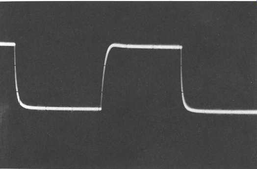
FIG. 12 (f) -(h) loss of HF gain.
The type of oscilloscope waveform shown in FIG. 12(e) would indicate a fall-off in gain at low frequencies, whereas that of FIG. 12(f) would show an increase in gain at LF. Similarly, the response shown in FIG. 12(g) would be due to an excessive HF gain, while that of FIG. 12(h) would indicate a fall-off in HF gain. With experience, the engineer is likely to recognize the types of output waveform which are associated with many of the common gain/frequency characteristics or design or performance problems.
The other types of waveform which can be provided by a function generator have specific applications which will be examined later. The sinewave output, though too poor in linearity to allow amplifier THD measurements to be made with any accuracy, is usually quite free from amplitude variation, and the 'single knob' wide-range frequency control of such an instrument allows fast checking of the performance of such circuits as low- or high-pass filters or tone controls.

FIG. 13 Origins of IM distortion.
DISTORTION MEASUREMENT
One of the more important characteristics of any audio system is the extent to which the signal waveform is distorted during its passage through the system. Where the input signal (f_in) is of a single frequency, and this distortion is due to some non-linearity in the transfer characteristics of the signal handling stages, this non-linearity will generate a series of further spurious signals occurring at frequencies which are multiples of the input frequency (or frequencies). Because these spurious signals have a harmonic relationship (i.e. 2/in, 3/in, 4/in, 5/in, etc.) to that of the input waveform this characteristic is known as harmonic distortion and, since all such harmonics will be present in the residue, it’s usually referred to as 'total harmonic distortion' (THD). Where the input waveform consists of signals at two or more distinct frequencies, a further type of distortion will occur, in which the amplitudes of each of the signals will be modulated to some extent at the frequency of the others - an effect which is more easily seen if there are only two input signals and these are widely different in both amplitude and frequency, as shown in FIG. 13. This type of distortion is known as Intermodulation Distortion' (IMD) and leads to a loss of clarity in the reproduction of such complex signals. Since, in audio applications, the input signal will be typically of multiple frequency form, IMD is very important as a design quality. There is, unfortunately, no direct numerical relationship between IMD and THD, except that the lower the THD of a system, the lower the IMD will also be.

FIG. 14 Parallel T notch filter characteristics.
THD meters
Two quite distinct techniques are used for such distortion measurement: Total Harmonic Distortion' (THD) meters and 'Spectrum Analyzers'. In the THD meter, the instrument is usually arranged so that there will be a sharp notch at some point in its gain/frequency curve, which will give zero transmission at some specific frequency, as shown in FIG. 14. If this notch is tuned to the same frequency as a low-distortion sinewave input test signal, then, when the test signal is 'notched out', what is left will be the spurious harmonics (plus hum and noise) introduced by the equipment under test, or the test instrument or the associated wiring connections.
In the normal method of use of this instrument, the 100% setting is found if the notch filter circuit is temporarily by-passed, its output is taken to a sensitive wide-bandwidth AC milli-voltmeter, and the system gain is adjusted so that the meter reads full scale. Then, when the notch is once more switched into circuit, the meter reading will show the residual THD + noise and hum.
In those cases where the intrinsic hum and noise in the system is fairly low, and the input test signal is a very low distortion sinewave - with, ideally, less than 0.01% THD - a simple THD measurement will often be entirely adequate to determine the performance of the equipment, particularly if the residual output signal waveform, following the notch circuit, is displayed on an oscilloscope.

FIG. 15 Crossover distortion residues.

FIG. 16 Distortion residues in high-quality audio amplifier

FIG. 17 Distortion from high-quality phonograph pickup.
With experience, the engineer can derive a lot of useful information about the circuit performance from this type of display. For example, in FIG. 15, the characteristic 'spikes' due to 'crossover distortion' in the output waveform of a relatively poorly designed (or badly adjusted) push-pull transistor amplifier can be seen very clearly in the THD meter output (and would, in practice, be audibly unpleasant), even though the waveform distortion which caused the spikes cannot be seen very easily in the output waveform shown above.
In FIG. 16 the THD meter output waveform shown is that from a high-quality high-power transistor amplifier at an output voltage swing, into a water-cooled resistive load, which is just below clipping level.
Because of some slight asymmetry in the operation of the amplifier under test - most probably in the output stage - there is a slight flattening of the lower part of the signal waveform, and this causes the slight undulation in the residual THD display which occurs at these negative-going peaks.
There are also some small crossover-type waveform discontinuities just visible in the THD trace, coincident with the mid-point of the voltage swing. The peak-to-peak amplitude of these is about the same level as that of the random background noise of the amplifier and meter. Because of their brief duration, they represent a very high order harmonic content -- probably the thirteenth or higher, and would, possibly be supersonic. Also, because of their brief duration, the energy associated with these glitches is very small. As a matter of interest, the actual harmonic distortion which was indicated for the amplifier test shown in FIG. 16 was 0.006%. A much more obvious distortion residue is that shown in FIG. 17. Since the THD residue waveform has twice the number of peaks as the input waveform it’s therefore due to the second harmonic. It was, in fact, measured as 0.65%, and was the output from a (high quality) phonograph pick-up replaying a 1 kHz test groove, cut at a lateral velocity of 5 cm/s on an vinyl LP test disc. The noise on the trace is surface noise from the disc.
A test signal of this kind is invaluable for setting the pick-up tracing angle, and, as shown, was almost certainly that when the cartridge was optimally adjusted.
As can be seen from the illustrations, a useful feature of this kind of measurement is that it allows the fault in the system to be related to that part of the signal waveform where it occurs. A disadvantage, also shown, is that the presence of high frequency circuit noise, as in FIG. 16, tends to conceal the error signals, while that of hum and low frequency noise as shown in FIG. 17 (in this case due to surface noise and 'rumble') blurs the display. For these reasons, most typical THD meters include optional low-pass and high-pass filters to lessen unwanted output artifacts. These filters are unsuitable for use at the low- and high-frequency ends of the audio spectrum, and lessen the usefulness of THD measurements under these conditions.
Almost any notch circuit can be used in an instrument of this kind, of which the two most popular are the Wien network nulling circuit, shown in outline form in FIG. 18, and the 'parallel T' notch circuit shown in Fig. 19. A practical circuit of my own (Wireless World, July 1972, pp. 306-308), based on a Wien bridge null network, is shown in FIG. 20. In order to get an accurate result the notch must be sharp enough to remove the fundamental frequency entirely, while avoiding any attenuation of the second harmonic frequency. In the circuit shown, the notch is sharpened up by the use of some overall negative feedback between the emitters of Q4 and Q1 via R13 and R6.

FIG. 18

FIG. 19
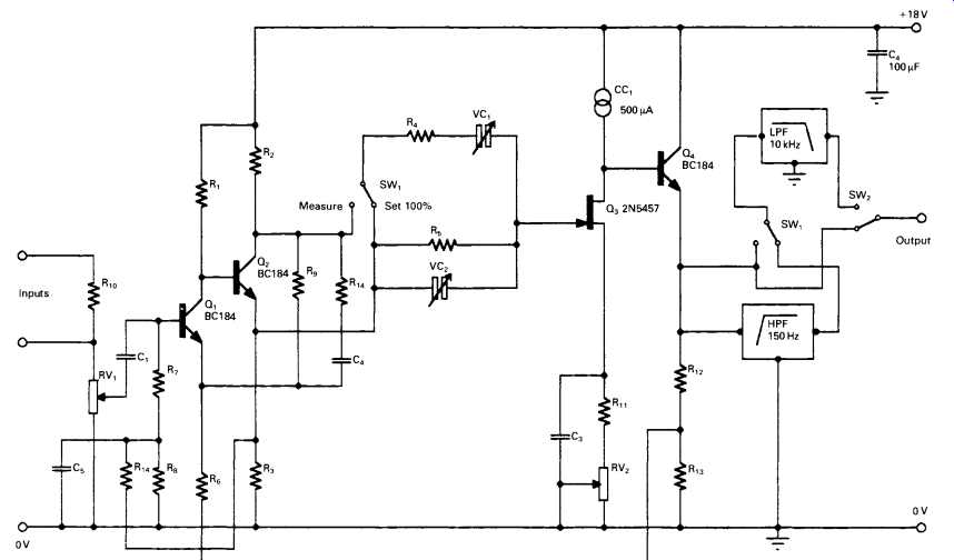
FIG. 20
IMD meters
As noted above, if the transfer characteristics of the system are non-linear, and there are two (or more) signals present at the same time, a further type of distortion will occur, as shown in FIG. 13. This is termed 'Intermodulation Distortion' (IMD), and arises because , for any signal, the gain of the system is defined by the slope of the transfer characteristic. This means that, for example, if a large signal is present at the same time as a smaller one, it will have the effect of moving the smaller signal up and down the transfer curve, and its gain, and consequently the size of the output voltage due to it, will change at the frequency of the larger one.
A variety of techniques are used to measure IMD of which the earliest (1961) was that proposed by the ( US) Society of Motion Picture and Television Engineers (SMPTE). In this two signals, typically 70 Hz and 7 kHz, at a 10:1 magnitude ratio, are fed to the system, the 7 kHz signal is separated by filtering and then demodulated to recover the 70 Hz intermodulation component which is measured using an RMS reading meter.
An alternative technique which allows the measurement of system performance in the 11-20 kHz region , for which harmonic distortion measurements would not be easily applicable, is the CCIR 'difference frequency' method in which two tones, of equal amplitude, at , for example, 19 kHz and 20 kHz are used as test signals, and the 1 kHz difference tone due to IM effects is isolated by filtering and measured. This type of test can be performed with various input signal frequencies, or even with the input signals swept over the 4-20 kHz range at a constant difference frequency (1 kHz or 70 Hz). A more recent approach, called the Total Difference Frequency' method, proposes test frequencies of 8 kHz and 11.95 kHz. The simple difference frequency product from these will be 3.95 kHz, while the second harmonic of the 8 kHz test tone will generate a 4.05 kHz difference frequency signal. Non-linearities at the HF end of the audio band are shown up by interactions between the third harmonic of the 8 kHz tone and the second harmonic of the 11.95 kHz one, which would produce a 100 Hz difference tone.
These high-frequency tests allow performance evaluations under dynamic conditions as distinct from the more usual single-frequency 'steady-state' tests. This is important, not only because components behave differently under rapid rates of change of operating conditions, and can malfunction in ways not found in steady state, but also because the bulk of the program material on which audio equipment operates is of a complex electrical form, rich in transients, and the skilled listener can readily detect alien sounds, within this total, due to system errors which may not be revealed by simple steady-state tests.
Spectrum analysis
The most powerful - but also the most complex, the most expensive and the most difficult to interpret - technique for determining system linearity is that known as 'spectrum analysis'. In the audio field, this is done by feeding the system with one or more input test tones, and then measuring the amplitude of all output signal components as a function of their frequency. This will immediately reveal both harmonics of the signal and their intermodulation products, usually shown graphically as amplitude on a logarithmic scale (dBV) as a function of frequency. A good instrument of this kind will allow the display of signal components as low as -120 dB, mainly limited by the noise floor.
Early instruments of this type used a layout, shown in simplified form in FIG. 21, which is somewhat similar to that of a radio receiver. In this, the input signal from the system under test, after amplification and buffering by a very low distortion input amplifier, is caused to modulate the amplitude of a swept frequency sine wave signal, typically in the 100 kHz range, which is then amplified by a very narrow pass-band HF amplifier.
The output from this amplifier is demodulated and converted into a DC voltage which is fed to a paper chart recorder to give the type of display sketched in FIG. 22. The frequency sweep system is coupled both to the chart recorder paper drive and to the variable frequency oscillator so that there will be a precise relationship between the frequency being sampled and the paper chart position. A fundamental problem with this type of instrument is that the response speed of the IF amplifier/demodulator system is directly related to the bandwidth chosen for the IF amp., so, if a high degree of spectral resolution is required (i.e. narrow IF pass-band) the sweep frequency rate and the chart drive speed (which are coupled together) must both be slow, perhaps requiring a minute or more for a complete 20 Hz to 20 kHz sweep.
Modern instruments for use in the audio band employ digital signal processing techniques based on 16 to 20-bit quantization resolution and sampling rates up to 204.8 kHz, depending on the application. The components of the signal under analysis are then resolved by fast Fourier transform (FFT) techniques. Typical contemporary instruments of this type are the Hewlett Packard 3562A, 35665A and 35670A dynamic signal analyzers. Instruments of this type are somewhat more rapid in response than the earlier swept frequency systems, with a typical high-resolution frequency spectrum, depending on the input signal frequency span, requiring less than a minute to display or refresh. A range of outputs would normally be available, including interface data for use with a computer, but if the output required is in the form of a graphical display, this would be provided by a laser or bubble jet printer. A typical numerical analysis of such an encoded FFT signal would allow, as , for example, in the Bruel and Kjaer 2012 instrument, the simultaneous graphical display of individual harmonic distortion components as a function of frequency - a facility which is very useful for loudspeaker, headphone or microphone design.

FIG. 21 Spectrum analyzer layout.

FIG. 22

FIG. 23 Typical oscilloscope display.
OSCILLOSCOPES
The remaining major class of test instrument in the audio engineer's laboratory is the 'cathode ray oscilloscope' - normally just called an 'oscilloscope' or 'scope'. This is an instrument which allows a voltage waveform to be displayed, visually, as a graph of voltage as a function of time. Normally, the horizontal axis of the display - the .Y-axis - will represent elapsed time, and the vertical axis - the Y-axis - will represent the signal voltage being displayed. The way by which this is done is shown, in a simplified manner, in Figs 23 and 24.
The oscilloscope tube has an electron source at one end, typically an indirectly heated thermionic 'cathode', from which a stream of electrons is drawn and accelerated towards a layer of fluorescent material, the 'screen', deposited on the inner face of the glass envelope of the tube. The internal electrodes in the tube cause the electron beam to be focused so that its region of impact on the screen generates a small, bright, point of light. If the target material is zinc sulphide, which is an efficient phosphor material, the emitted light will be of a green color. Other colored screens are available, but green is preferred by most engineers as a restful color for extended viewing. A group of four deflection plates is interposed between the electron source and the screen as shown in FIG. 23, and the lateral or vertical position of impact of the electron beam on the screen will be controlled by the voltages present on these plates at the instant when the individual electrons forming the stream pass between them.
FIG. 24 Timebase scan waveform.
In a simple 'scope, the horizontal scan voltage will be a 'sawtooth' waveform of the kind shown in FIG. 24. In principle, this could be generated by a 'function generator' IC, but in practice, since it’s essential that the voltage waveform is extremely linear between points A and B, and occupy as little time as practicable in returning from point B to point C to begin the cycle again, 'scope manufacturers will normally provide their own discrete component circuitry for this purpose, though there will usually be an external electrical input point to allow the user to supply his or her own horizontal scan waveform, when needed. (Since it’s desirable to avoid confusion of the display due to the presence of extra images during the scan return from B to C, the trace is usually blanked out during this period.) The voltage waveform which it’s desired to display is then applied, after suitable amplification, to the Y plates, which causes the electron beam to be deflected vertically, to an extent which is accurately related to the applied voltage.
The vertical or horizontal position of the display on the tube screen is controlled by the application of a suitable DC voltage to the plates, normally called the 'A'-shift' or ?-shift' controls. To preserve the sharpness of the spot focused on the screen the electronic circuitry of the X and Y amplifiers is chosen so that the voltages applied to the deflection plates are in 'push-pull' (i.e. equal in magnitude but opposite in polarity). To allow some fine trimming of the focus and deflection voltages , for optimum spot sharpness, an 'astigmatism' control will usually be provided.
The length of time which is occupied in traversing from A to B will determine the time axis of the display, so that , for example, if the waveform displayed on FIG. 23 as a result of an alternating voltage applied to the Y plates is a 1 kHz sine wave (i.e. 1 ms/cycle), then the horizontal (X-axis) time scale will be 5 ms, which would imply a 200 Hz repetition rate for the X waveform. The ability of the 'scope to display very high-frequency input waveforms is limited only by the ability of the 'scope electronics to charge and discharge the stray capacitances associated with the plate electrodes, through the inevitable inductances due to the plate connecting leads.
Generally, the 'scope time base generator circuit will allow the user to choose the X-axis repetition frequency, as a switchable sequence of scan times, ranging, perhaps, from 10 s/cm to 0.1 µ^?t?. There will also be a control which will allow some variation in these pre-set speed settings to facilitate synchronization of the signal being displayed with the horizontal scan speed. On some 'scopes, there will also be an option which will enable the user to increase the scan width by a factor of 10. Since the repetition rate remains the same, the effect of this will be to leave the waveform synchronized with the horizontal scan, but to spread this out so that the time component of the waveform can be seen in greater detail, since the X-shift control will allow the waveform displayed to be moved horizontally. The facility of expanding a small portion of the X trace, to speed up part of the display, while leaving the remainder unaffected, is still sometimes offered, as has been the ability to display different traces at different scan speeds, but these are unusual facilities.
An interesting curiosity in this field is that the spot of light on a 'scope screen is able to move at a velocity which is greater than the speed of light -- because it’s not itself a physical entity, merely a historical record.
The X and Y amplifiers, which amplify the time base and y input signals before presentation to the deflection plates, are generally similar in sensitivity and bandwidth, to facilitate the use of either of these inputs for signal purposes. A normal maximum y input sensitivity will be in the range 1-10 mV/cm, with a bandwidth of up to 100 MHz, depending on the cost and performance bracket of the instrument. For audio use a 2 mV/cm sensitivity and a 10-20 MHz bandwidth would be quite adequate. The need for such a high HF bandwidth arises because, particularly with MOSFET devices, circuit instabilities may lead to spurious oscillation in the 5-20 MHz range, and it’s desirable that the 'scope should be able to show this, when it’s present.
It’s also normally expected that the Y amplifier should be 'direct coupled', so that a DC voltage can be displayed as a vertical offset of the horizontal scan position. The 'shift' voltages are added to the y (or X-axis) signals, after the input attenuation, so that the required scan position can be obtained under signal input conditions where both AC and DC inputs are present. If it’s preferred to ignore the DC component of the signal, an input blocking capacitor can be switched into circuit. The 'direct coupled' input facility is very useful for measuring small DC offset voltages in sensitive regions of the circuitry.
Multiple trace 'scope displays
With the exception of small, portable or battery operated instruments, almost all modern 'scopes offer multiple 'trace' displays, which enable two or more Y-axis signals to be shown simultaneously, one above the other on the screen. This facility is exceedingly valuable, in that it allows the comparison of the input and output waveforms from any system under test, so that changes in waveform shape, or delays in time between input and output, can be seen immediately.
When using a simple notch-type THD meter, a dual trace display is also very helpful in that the input waveform can be shown on, say, the upper trace, and used for display synchronization, while the noise and distortion residues are displayed on the other. Not only does this allow the identification of the position on the waveform at which the defect occurred, but it also prevents the loss of synchronization which would otherwise take place when the input waveform was 'notched out'. With systems using digital signals multiple trace displays allow the timing of a number of output or input pulse streams to be checked, though this is an area somewhat outside the scope of this book.
In early 'scopes, the provision of multiple trace displays was achieved by the use of separate electron 'guns', focusing electrodes and X and Y plate assemblies, but this made for bulky and expensive CR tubes. In modern 'scopes, the technique employed uses a combination of fast electronic switching applied to the input signal in synchronism with a superimposed square wave vertical deflection waveform of adjustable size. This allows one or other of the input signals to be switched to the Y amplifier, and thence to the Y deflection plates, at a vertical display position determined by users by that choice of square wave size. The display sequence may be either 'alternate', in which sequential '^-axis' sweeps are chosen to display alternate inputs, or 'chopped', in which the input waveforms are rapidly sampled, during the sweep, and routed, up or down, to the chosen display positions.
Normally the choice of trace division technique is determined automatically by the 'scope circuitry according to the A'-axis sweep speed selected. At low sweep speeds, the input waveforms will be chopped at a frequency which is high in relation to the signal frequency. This would be preferable , for example, if it was desired to do time comparisons between waveforms from different Y inputs. For high-frequency signals, alternate displays are normally selected, on the grounds that the persistence of vision will make the display seem continuous. The accuracy of the relative horizontal position of such a display is, in this case, dependent on the freedom from 'jitter' of the time-base synchronization.
Time-base synchronization:
The ability to 'freeze' a repetitive waveform on the 'scope display is an essential quality in any oscilloscope, and facilities are invariably provided to allow trace synchronization with any specified signal input, but also from an external 'sync' input. Various types of synchronization are also usually provided by switch selection, in the hope that some of these may be more effective that others. My choice of words is prompted by the experience, over many years and with many 'scopes, that some 'scopes and some waveforms can prove very difficult to lock on the screen. In fact, one of my personal priorities in the choice of an oscilloscope is ease of synchronization. Sadly, one only ever discovers whether this is good or poor after the purchase of the instrument - unless one has had previous experience with that make and model.
External X-axis inputs and Lissajous figures
The input to the X-axis amplifiers can usually be disconnected from the output of the sawtooth waveform generator and taken from an external 'Time Base Input' connection. This then allows a single-beam 'scope to be used to display 'Lissajous figures' of the kind shown in FIG. 25. In the ring-shaped display of FIG. 25(a), the external X input and Y inputs are at the same frequency, though at phase quadrature. If they are in phase, or in phase opposition, the resultant display will be a straight line at 45° or 135° to the horizontal axis.

FIG. 25 Typical Lissajous figures.

FIG. 26 Mono/stereo signal display.
In FIG. 25(b), the X input is at twice the frequency of the Y one, while in FIG. 25(c) the Y input is twice the frequency of the X input. In FIG. 25(d) the X input is three times the frequency of the Y input -- and so on.
This provides a rough and ready means of assessing the frequency of an input sinusoidal signal if one has a calibrated sine wave source. However, small frequency drifts in the signal inputs lead to continuous snake-like inter-twinings of the display, which makes the precise determination of frequency difficult to achieve.
With a dual trace oscilloscope, the same result may be obtained more easily by displaying the signal of unknown frequency, in synchronism on one trace, and then using the second trace to display the output from a variable, but calibrated signal generator. Apart from the difficulty of obtaining simultaneous synchronization, the unknown frequency can be determined from noting when both traces display the same number of cycles.
An interesting application of the Lissajous principle is shown in FIG. 26, where the LH and RH channels of a stereo signal, such as , for example, an FM tuner, are connected to the X and Y inputs of the 'scope.
A mono signal will give the kind of display shown in FIG. 26(a), where the length of the line display will depend on the magnitude of the input signal.
On a speech or music input, a stereo signal will give the kind of display shown in FIG. 26(b), where the extent of the 'roundness' of the pattern is an indication of the extent of the image separation of the two channels.
This allows the adjustment for maximum channel separation of an FM stereo decoder , for example, without the need to seek special test signals.
'X-axis' signal outputs
Most 'scopes also provide a 'time-base output' socket, at which the 'X-axis' scan voltage waveform ( FIG. 24) is available. This is required for controlling the frequency sweep of the voltage controlled RF oscillator in a frequency modulated oscillator, or 'wobbulator', whose use was described in SECTION 2 (Tuners and Radio Receivers), and for which the output waveforms were shown in Figs 41-43. A similar system is used for the 'Panoramic' display of radio signals as a function of frequency.
Digital storage oscilloscopes
Oscilloscopes, like all other electronic test equipment, has become more versatile, more complicated and more expensive with the passage of time, and this development is particularly notable in the field of 'storage' oscilloscopes, which allow the provision of numerically stored displays.
The ability to 'freeze' a transitory waveform, so that it could be measured or examined at leisure, has been sought for very many years, and early instruments endeavored to meet this need by the use of long-persistence screen phosphors, which would continue to display the screen waveform, though at a much reduced brilliance , for a minute or more following switch-off. An improvement on the performance of long-persistence screens was obtained by the use of a dual-phosphor screen coating, in which a normally dormant phosphor layer could be reactivated to display its last image, by flooding it with infra-red radiation. However, contemporary digital technology, and fast A/D converters, offer the ability to capture and store the actual signal in numerical form - information which is refreshed each scan. In the technique used, the incoming signal is repetitively sampled, at a rate which is high in relation to the horizontal sweep speed, and the instantaneous signal voltage level is stored for a time which is long enough for its value to be noted and transformed (quantized) into a digitally encoded form.
This instantaneous numerical equivalent to the input signal amplitude is then stored in a fast random access memory store, while the output from a digital-to-analogue converter (DAC) is simultaneously displayed on the oscilloscope screen. The advantage of this type of display - apart from the convenience of being able to examine a possibly transient waveform at one's leisure - is that, once the signal is in digital form, a wide range of mathematical manipulations may be performed on it. An example of this is the Fast Fourier Transform process noted above in relation to spectrum analysis. The stored signal can also be fed to a computer or printer for an immediate hard copy.
It’s also common, with modern digital storage oscilloscopes, to use the microprocessor system within the control electronics to show the X-axis time scale on the 'scope display, as well as the DC and AC parameters, including frequency, of the input signal(s). Input signal sampling rates of up to 500 Mega-samples/s are available in top-range instruments - though these are expensive. Vertical resolution equivalent to '8-bit' encoding (±0.15 mm on a 100x125 mm tube face size) is typical.
Modern test instrumentation of the various kinds described above allows a great deal of information to be obtained about the electrical characteristics of audio equipment. However, as indicated at the beginning of this SECTION, our understanding of the relationship between the measured performance and the quality of sound produced by the equipment under test is still less comprehensive that we would wish, and innovations in technology, particularly in the field of digital audio, continually pose new questions about the acoustic significance of those imperfections which remain.