The next time you undertake to design your own digital project, let this unique device provide you with regulated + 5- VDC power, with LED current monitor, two logic probes, and 12 clock frequencies from 0.01 to 170K Hz
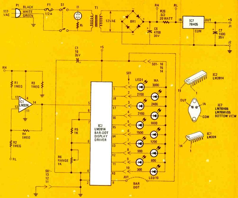
--------FIG. 1. THE POWER- SUPPLY PORTION of the Digital Prototyping System
uses a simple bridge rectifier to supply power to the 5-volt DC regulator
chip, IC7. Resistor R26 senses the current used at the output and displays
that miniscule voltage drop across the bar-dot display driver, IC2. With
jumper JU1 installed, a bar display will indicate current ii 300 mA steps
very much like a rising thermometer.
REMEMBER THE LAST CIRCUIT THAT YOU BUILT ON A SOLDER-less breadboard? The wires were running off the block every- where, and were connected to a makeshift power supply. A quick twist of the wires, insulated by precisely angled bends, is all that was needed so that the bare conductors never touched, but somehow did! Once the power supply is deemed reliable, it is a simple matter of juggling a logic probe around in a manner as to be most effective for debugging. All the while keep in mind that power cord movement must be kept to a minimum, thus preventing excessive testing and repairing of the power supply.
The Digital Prototyping System described here provides a 5-VDC, 3- ampere regulated power supply, with an LED current monitor. Two digital logic probes with memory are added to prevent wire-lead clutter and to make it hard to misplace the probes. Each probe can detect pulses as short as 40 nano-sec. An adjustable clock with several divided-down outputs is included to help streamline breadboarding time and to eliminate wasted space on the block.
The power-supply circuit
The power- supply circuit is shown in Fig. 1. Transformer T1, bridge- rectifier BR 1, and filter-capacitor C6 form a full-wave power supply regulated by IC7, a 78H05 high-current regulator integrated chip, and capacitor C7. The output is rated at 5-volts DC into a 3- ampere load maximum.
The current monitor uses a .5-ohm, 20-watt resistor, R26, to cause a voltage drop equal to .5 millivolt per milliamp of-ML output current. Two 1-ohm, 10-watt resistors were used in parallel to form R26. The internal current used by the 78H05 regulator, IC7, is small enough to be ignored. That proportional voltage across terminal points RH and RL is fed into IC1 , a LM324 unity-gain op amp, that ground- references the signal so that any voltage drop on the unregulated side of the power supply will not affect the current reading. IC2 is a LM3914 bar-dot display driver. The input divider is calibrated to read 300 mA per LED by resistors R5 and R6. Pin 9 on IC2 selects either a bar or dot display. Connecting pin 9 to +5 volts DC will select the bar mode.
The regulator, IC7, can put out slightly more than 3 amperes for short lengths of time. Prolonged use above 3 amperes will cause early failure of the transformer or bridge rectifier unless they are rated well over 3 amperes. The regulator, IC7, is internally protected against short circuits that draw more than 5 amperes. Staying within those limits should insure long life of the power supply.
Double logic
The two logic probes are identical and are shown in Fig. 2. Half of 1C3 and IC4 make up each probe. The operation of only one probe will be described here. The other probe works the same way, and is totally independent of the first. The numbers shown in parenthesis are symbol and pin designations for the second probe.
NPN transistors 2N3904, Q1 and Q3, along with two sections of hex inverter 74LS04, make up the state detector for the logic probe. Transistor Q3 turns on during low pulses causing IC4-b to go high and turning on the Low LED indicator, LED13. When the input of Q3 is high or floating, the input of IC4-b is pulled high by resistor R13 and holding the Low LED off.
The high- detection circuit is much the same. The input of IC4-a is held low through resistor R11 whenever the base of Q1 is low or floating. When a high is applied to the probe's input, Q1 turns on pulling up the input of IC4--a and turning on HIGH LED, LED 11 .
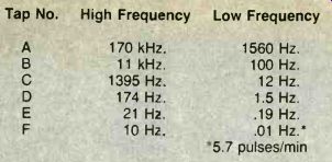
TABLE 1--CLOCK RANGES Tap No. High Frequency Low Frequency
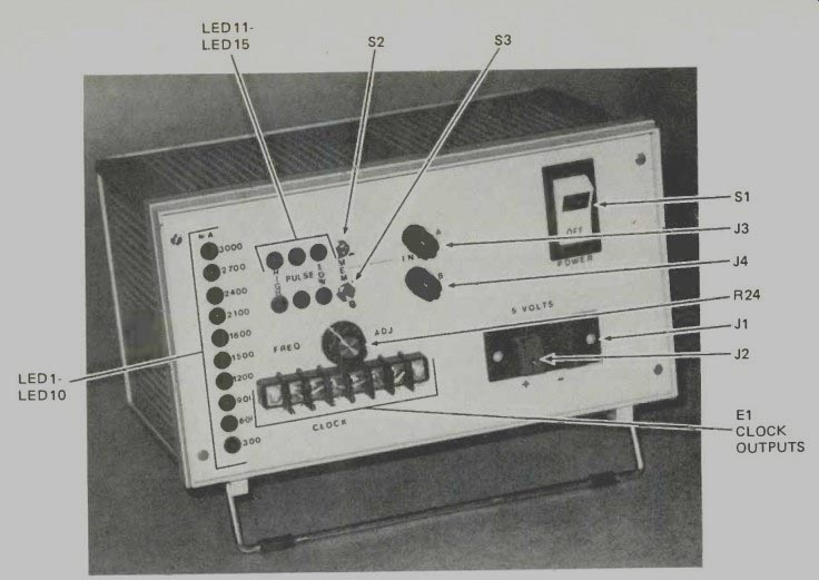
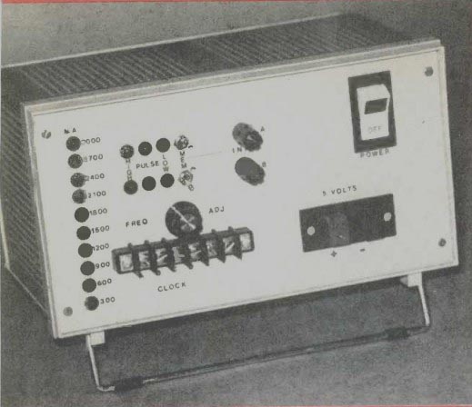
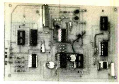
---- THE DIGITAL PROTOTYPING SYSTEM is as rich looking as its name sounds.
Light- emitting diodes LED1 through LED10 indicate current supplied to
an external- connected project in steps of 300 milliamperes. Clock outputs
offer six frequencies from 170 kHz to 10 Hz at high setting of FREQ ADJ
potentiometer R24 at maximum and 1560 to .01 Hz. (approximately 5.7 pulses
per minute) at the minimum setting. Two independent and separate pulse-probe
circuits are provided with suitable high- and low-state indicators with
pulse memory. Of course, there's the 5-volt regulated power supply terminals
and POWER ON /OFF switch S1-the brutish, but ever so essential, purpose
of the Digital Prototyping System.
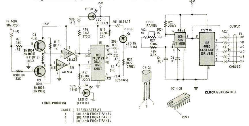
FIG. 2. THE LOGIC AND CLOCK PORTION of the Digital Prototyping System could
be separate projects by themselves. The clock section offers six time-related
clock signals for intervals listed in Table 1. The logic-probe section actually
consists of two identical probes. The diagram lists symbol and pin designations
for one logic probe, and another set of designations in parentheses for
the second probe.
---JUST SITTING THERE doing nothing makes the circuit board section of
this project seem simple. Nevertheless, it would b: wise to resort to a
printed- circuit board for construction instead of using point-to-point
wiring.
Short-pulse detection and memory are provided by IC3-a, a 74LS123 one-shot chip. IC3-a is triggered by a high to low transition of IC4-b or a low to high transition of IC4-a. The Q output remains low for a time determined by resistor R19 and capacitor C2, past the last trigger pulse. The pulse time is approximately 250 msec. with the values given for R49 and C2. Pulse memory is accomplished by closing PULSE switch, S2. The low pulse from the Q brought to the junction of C2 and R19 preventing the capacitor from charging and holding the one-shot in its triggered state, with PULSE LED, LED15 on. Opening S2 causes C2 to charge and after 250 msec. Q goes high and the PULSE indicator, LED15 goes out.
Tick tock
The clock circuit is made up of IC5 and IC6. See Fig. 2. IC5 is a 555 timer connected in its astable mode. The frequency is adjustable by range potentiometer R24. The output of the timer is fed to IC6, a 4060 CMOS 14-stage binary divider chip. The input signal is divided down and tapped off at five different stages. That allows the clock output to be available at six different frequencies simultaneously. The available range is from + 170 kHz to less than .1 Hertz. The clock ranges are listed in Table 1.
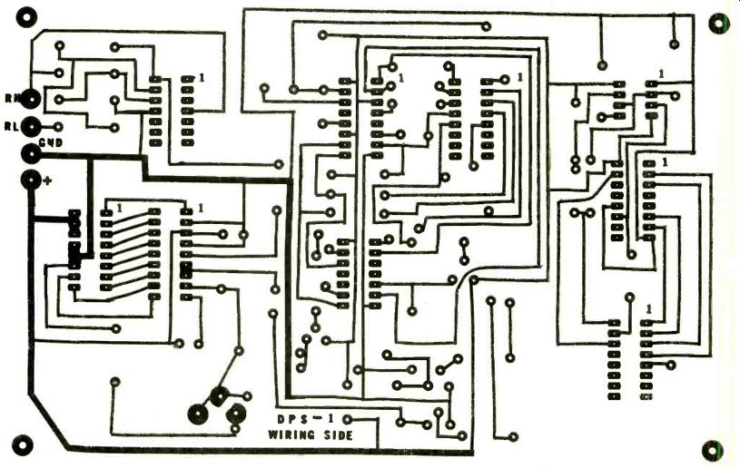
FIG. 3. HERE IS THE ART for the foil side of the printed- circuit board.
The use of the PC board is the only sure way to go.
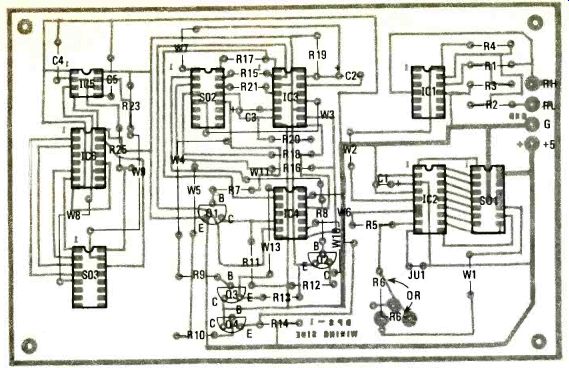
FIG. 4. PARTS LOCATED on the PC board are shown along with wire jumpers
and the bar-dot jumper JU1. With JU1 connected, the light- emitting diodes
will remain illuminated for a bar display. The foil pattern is shown
in an x-ray view.
Construction
The main circuit can be assembled using an etched printed-circuit board, or a wire-wrapping technique on a perf- board.
A foil pattern of the wiring side of the PC board is shown in Fig. 3. Component placement is shown in Fig. 4.
Mount all PC components to the board, making sure of proper orientation of the IC sockets, and capacitors. Make sure that all wire jumpers are installed.
Due to the wide variety of component sizes available, the power supply is mounted on a terminal strip as shown in Fig. 5. Capacitor C6 is not a critical value; the bigger, the better.
Any value from 3,000 to 10,000 µF at 35 volts will do the job. If other than the specified transformer and bridge rectifier are used, make sure they can handle the current. If the value of C6 is above 5,000 ¡4F then the bridge should be rated at least 5 amperes. Otherwise, the high inrush of current during power-up could cause early failure of the rectifier The 78H05 regulator, IC7, must be mounted on a finned heat sink, as it will he dissipating around 25 watts at 3 amperes output. Use heat-sink compound when mounting the regulator to the heat sink. If the heat sink is mounted inside the chassis, then adequate ventilation must be provided. The case of the regulator is ground so it is safe to mount it to the back of the chassis where the cooling will be the best.
Measure the four 1,000,000-ohm resistors, R1-R4 with an ohmmeter. Use the one with the highest value for R4 for best circuit operation. Measure the output of the op amp, IC1, with no load on the power supply. The offset should be less than 11 mV. Some experimentation with the value of R4 may be necessary. It must be higher than R1 to ensure a low enough offset.
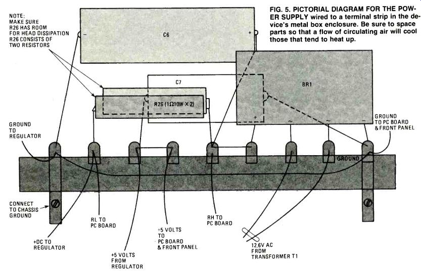
FIG. 5. PICTORIAL DIAGRAM FOR THE POWER SUPPLY wired to a terminal strip
in the device's metal box enclosure. Be sure to space parts so that a flow
of circulating air will cool those that tend to heat up.
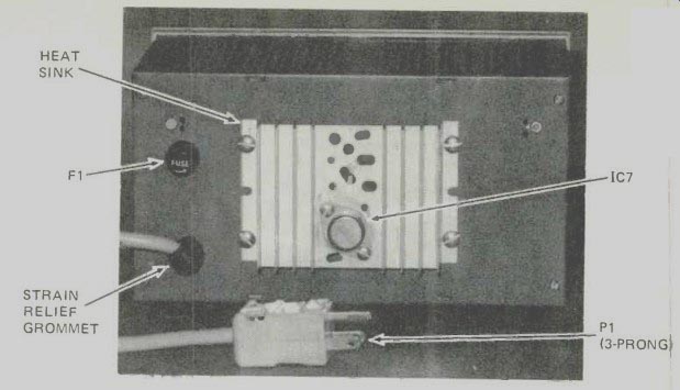
-------- A PEEK AT THE BACK of the unit shows the 5-volt regulator
chip mounted on an over-sized heat sink which is OK considering that
the heat sink was taken from the junk-box. Fuse location is satisfactory
and strain relief on the power corn is very good construction practice.
A grounded three-wire electrical cord with molded plastic plug P1 is necessary to insure personal safety. The ground should be bonded, (good electrical contact) to the chassis with a nut, lock washer, and bolt.
The transformer or terminal strip mounting bolt is a good place for the ground. The power- supply ground return should also be connected to the chassis at the same point.
All the front-panel parts are connected to the PC board by DIP jumper cables. The wires are soldered to the front panel parts and the PC-board ends plug into 16-pin IC sockets.
==========
PARTS LIST FOR DIGITAL PROTOTYPING SYSTEM
SEMICONDUCTORS
IC1--LM324 operational amplifier (op-amp) integrated circuit
IC2--LM3914 bar-dot display driver integrated circuit IC3- 74LS123 dual one-shot integrated circuit IC4-74LS04 hex inverter integrated circuit
IC5--LM555 timer integrated circuit
IC6--4060 CMOS 14- stage driver integrated circuit
IC7--78H05 5-volt DC regulator integrated circuit
BR1-6-A, 50-Ply bridge rectifier module (Radio Shack 273-1180 or equivalent)
LED 1--LED, 16-Light emitting diode, red, 20 mA forward current
Q1, Q2--2N3904 NPN transistor
Q3, Q4--2N3906 PNP transistor
RESISTORS
All resistors are 1/4-watt, 5% unless otherwise specified
R1-R4--1-Megohm R5, R13.
R14--1000-ohm
R6--1000-ohm trimmer potentiometer
R7, R8, R19, R20--33.00-ohm
R11, R12--100-ohm, 1/2-watt
R15-R18. R21-R23--270-ohm
R24--500,000-ohm potentiometer
R25--3,300-ohm
R26-0.5-ohm, 20-watt (use two 1-ohm, 10-watt resistors in parallel)
CAPACITORS
C1--10-µF, 35-WVDC electrolytic
C2, C3--.47-uF disk
C4--.001-µF disk
C5--.01-µF disk
C6- 4700 µF, 35-WVDC electrolytic
C7--1000-µF, 35-WVDC electrolytic
ADDITIONAL PARTS AND MATERIALS
E1--6- terminal, barrier-type, screw-mount strip F1--1/2-A fuse and holder 11-Neon panel indicator light with built-in dropping resistor J1, J2-Quick connect/disconnect, color-coded binding terminals (type used for rapid connect to speaker leads)
J3. J4--Multi-way binding posts, black
S1--DPST power switch
S2-S3-SPST miniature toggle switch
T1-Low-voltage power transformer; 117-VAC primary winding; 12 6-VAC. 3A secondary winding with no center tap 3- Cables, ribbon-type with 16 leads, terminal one end in 16-pin DIP jack to mate with 1E-pin DIP IC-type socket 1- Heatsink for I07. 50-watts dissipation minimum (Radio Shack 276-1361)
Printed-circuit fabrication materials, mounting hard- ware, knob, case, heatsink compound, terminal strip, solder, wire, line cord with molded 3-prong AC plug (P1). etc.
An etched and drilled printed- circuit board is avail- able from Micro Power Systems, RFD *2, Rt. 4-A, Enfield, NH 03748. Price is $11.50 and includes ship- ping and handling charges. Please note: All boards shipped UPS unless otherwise specified. Visa and MasterCard accepted. Be sure to give all information on card.
==========
Calibration and checkout
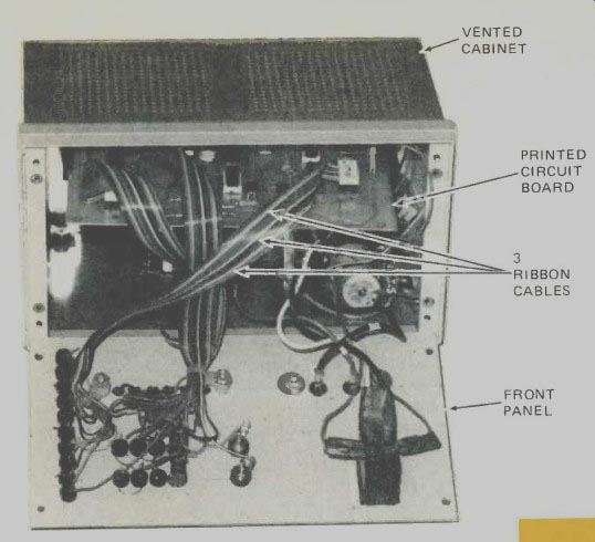
------------ DROP THE FRONT PANEL and the interior looks like a well-
designed project with good construction practice. Ribbon cables are used
to interconnect components on the front panel with the printed- circuit
board.
Thus, in the event that faulty wiring occurs in construction, it can be quickly traced by using the cable's color code. The printed- circuit board is held in place by holders specially designed for that purpose. However, you may want to go the less ex- pensive route by using low-cost standoff posts which do the same job at a fraction of the cost.
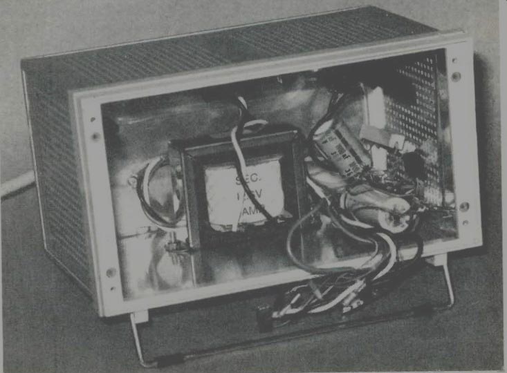
--------- WITH THE FRONT PANEL completely removed and the printed-circuit
board slid out of its holders, the project looks very much like a simple
power supply--which it really is! The add-on circuits make the unit extremely
valuable to the circuit designer and prototype, who must monitor Vc,
current and have knowledge of the switching action in the externally-powered
circuit.
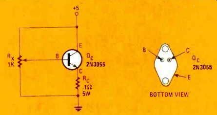
FIG. 6. HERE'S A SIMPLE CALIBRATION LOAD for the Digital Prototyping System.
Make brief current tests of 15 seconds or less; otherwise, the transistor
will overheat. Even a brief test will raise the transistor case temperature
sufficient to burn flesh.
The only adjustment is for the current monitor. The volt- age at pin 6, IC2 should be set equal to the voltage at pin 5 during full rated output (3 A). A simple calibration load is shown in Fig. 6. Connect a DC ammeter, capable of displaying 3 amperes, in series with the calibration load as shown.
Adjust Rx until the meter reads 3 amperes. Using a DC voltmeter, measure the voltage at IC2, pin 5. Record the voltage and disconnect the load. Now move the voltmeter to pin 6 and adjust R6 until the voltage reading is the same as at pin 5. All voltage measurements are taken with reference to ground.
Be cautious around Q, (Fig. 6) as it is dissipating 15 watts and will get very hot without a beat sink. Severe burns could result if the transistor is touched. If not using a heat sink, then disconnect the positive lead that goes to the power supply every 15 seconds to allow the transistor to cool to a safe temperature.
The checkout of the logic probes is simple. With the power supply turned on, touch one probe to the + 5 terminal. The HIGH LED (LED 11) should go on and the PULSE LED (LED15) should stay on for only about 250 msec. Touching the probe to ground should light the Low LED (LED13) and the PULSE LED should flash when the probe is removed from ground. With the memory switch, S2, on, touch the +5 bus and then ground the probe. The pulse LED should go on and stay on even after the probe is removed from the signal.
When the switch is turned off the PULSE LED (LED 15) should extinguish about 250 microseconds later. Both probes work in the same manner and can only be used for TTL and positive CMOS circuits.
The clock frequency is adjusted by potentiometer R24. By selecting a range tap and changing the setting of R24, any desired frequency can be obtained within the range selected.
The outputs B through F are CMOS outputs with a 5-volt swing. External buffering may be necessary for some circuits. The 4060 CMOS divider chip, IC6, has a fan out of 2 74LS loads, and cannot drive 7400 TTL devices directly.
The Digital Prototyping System should give you everything you need to easily design many more projects in the future. Debugging is also a snap due to the elimination of all the extra leads and wires that normally clutter up a bread-board.
by: ALAN BRADFORD
= = = =
Radio-Electronics--Special Projects (USA print magazine)
Also see: Single Sweeper One