AMAZON multi-meters discounts AMAZON oscilloscope discounts
Many types of transistor amplifiers are used in various applications. This Section explains only the simpler types of amplifiers, and the waveforms associated with amplifier circuit action. RC coupling is used extensively with junction transistors. In Fig. 4-1A, R1, C1, and R2 form the RC network be tween the two transistor stages. C1 blocks DC and couples the ac signal; R2, the DC return resistor for the input element of the second stage, develops the signal applied to the input of the second stage. C1 prevents the DC voltage on the collector of the first stage from appearing at the input terminal of the second stage.
Note that the reactance of the coupling capacitor (which is in series with the low-valued input resistance of the following stage), must be small compared with the input resistance.
Otherwise, an excessive amount of signal voltage will be dropped across the capacitor. A high value of capacitance is used because the input resistance of the following stage is low-usually lower than 1000 ohms. However, the physical size of the capacitor is comparatively small because of the low volt ages in the circuit. The ohmic value of the DC return resistor is usually 7 to 15 times the value of the transistor's base input resistance of the second stage. This fairly high ratio of resistance is necessary to prevent shunting an objectionable amount of signal current around the input circuit of the second stage.
Since the reactance of the coupling capacitor increases as the signal frequency decreases, the very low frequencies are attenuated. The shunting effect of the collector-emitter capacitance of the first stage, and the base-emitter capacitance of the second stage limit the high-frequency response of the amplifier (assuming that the transistor is of a type that is capable of amplifying the high frequencies). Any transistor is rated for a beta cutoff frequency by the manufacturer, and may also be rated for an alpha cutoff frequency. In either case, the cutoff frequency of the transistor is determined by the frequency at which the response is down 3 dB, in an amplifier circuit that is capable of processing frequencies past the cutoff point of the transistor. It is found that the alpha cutoff frequency of a transistor is often higher than its beta cutoff frequency. Therefore, a transistor may be used in the CB configuration when very high frequencies are to be processed.
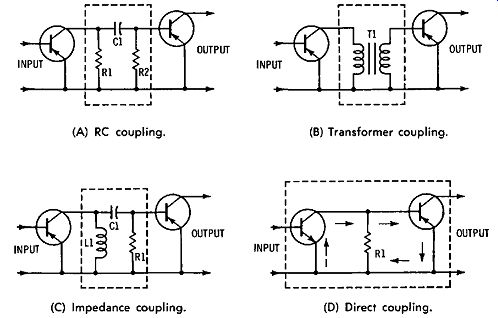
Fig. 4-1. Interstage coupling networks. (A) RC coupling. (B) Transformer coupling.
(C) Impedance coupling. (D) Direct coupling.

Fig. 4-2. Transistor circuit parameters. (A) Common emitter. (B) Common base.
(C) Common collector.
The efficiency of an RC-coupled amplifier is equal to the ratio of ac power output to DC power supplied to the stage. This efficiency value is rather low, due to the I^2R power loss in the collector load resistor. Other amplifier configurations provide considerably greater efficiency. RC coupling is used to a large extent in audio amplifiers, as in low-level low-noise preamplifiers, in driver amplifiers, and in high-level power amplifiers.
The chief advantages of RC amplification are high gain, production economy, and compact construction. Because batteries such as are used in portable equipment have limited current capability, this type of equipment is generally limited to low power operation. Fig. 4-2 shows a summary of the principal parameters of single-stage transistor amplifiers.
FREQUENCY RESPONSE OF RC-COUPLED AMPLIFIERS
Simple RC-coupled amplifiers have maximum gain over their midband region, with reduced gain at the low- and high-frequency ends of their response range. Low-frequency gain is limited chiefly by the increasing reactance of coupling capacitors at low frequencies. High-frequency gain is limited by the bypassing effects of stray circuit capacitance and junction capacitances of the transistors. Therefore, regardless of the particular R and C values, the frequency response of any RC coupled amplifier is the same with reference to a universal RC frequency-response curve. For example, Fig. 4-3 shows the low-frequency response curve for a single RC-coupling circuit.
The percent of maximum amplitude is directly proportional to frequency, resistance, and capacitance.
Note that the frequency-response curve in Fig. 4-3 is shown in semilog coordinates. The reason for this is that low-frequency sweep generators commonly have a semilog time base; therefore, the curve that is displayed on the scope screen has the aspect shown in Fig. 4-3. The only difference between a semilog time base and a linear time base is that the left-hand region of the pattern is expanded, or "stretched out." This is desirable when the cutoff characteristic of an amplifier is comparatively steep, because the operator can read voltage values more accurately. Of course, the same data are displayed, whether a scope employs a linear time base or a semilog time base.

Fig. 4-3. Universal frequency-response curve for RC-coupling unit.

Fig. 4-4. Universal frequency-response curve for two-stage RC-coupled amplifier.

Fig. 4-5. Universal RC frequency-response curve for single-stage amplifier.
When two RC-coupled stages are connected in cascade, the output from the first stage is multiplied by the amplification of the second stage. In other words, the amplitude values depicted in Fig. 4-3 are squared by the second stage; this rule assumes that the same RC values are used in both the first and the second stages. Fig. 4-4 shows the low-frequency response curve for a two-stage RC-coupled amplifier. Note that Figs. 4-3 and 4-4 depict the low-frequency end of the frequency response curves. The output rises to 100 percent through the midband region. At the high-frequency end of the frequency response, the output drops, due to stray capacitance and junction capacitance that shunts the collector load resistor. To measure the total output capacitance, we must use an impedance bridge.
If we know the value of the total output capacitance, and the output resistance (value of the collector load resistance in shunt with the transistor's collector-output resistance), we can find the frequency response at the high-frequency end of the range from the universal RC frequency-response curve given in Fig. 4-5. This is the high-frequency response curve for a single-stage amplifier. In most cases, we will not know the exact values of RT and CT. Therefore, we simply check the frequency response with a sweep generator and scope instead of calculating the frequency response. Nevertheless, it is instructive to know how the frequency response can be calculated.
When two stages are connected in cascade, with the same type of transistors, and the same values of collector load resistance in each stage, the output from the first stage is multiplied by the amplification of the second stage. In other words, the output from a two-stage amplifier is equal to the square of the amplitudes depicted in Fig. 4-5. In turn, the two-stage output is shown by the universal frequency-response curve given in Fig. 4-6.
Note in Fig. 4-6 that the R value in w RC can be taken as equal to RL, provided that the collector-output resistance and the base-input resistance of the transistor are comparatively high. In most amplifiers, the value of RL is sufficiently high that we must calculate the value of R; in this case, the value of R is equal to the parallel combination of RL, the base-input resistance of Q, and the collector-output resistance of Q. Of course, the total base-input resistance is equal to the parallel combination of the base return resistance and the input resistance looking into the base of the transistor. As before, CT (Fig. 4-7) is the total shunt capacitance in the collector circuit, and is equal to the sum of the stray circuit capacitance, the collector junction capacitance, and the base junction capacitance.

Fig. 4-6. Universal frequency-response curve for two-stage amplifier.

Fig. 4-7, Internal capacitances of a junction transistor.
Fig. 4-8 shows the frequency response of a typical audio amplifier from 20 Hz to 20 kHz. A low-frequency rise is present in this example, due to misadjustment of the low-frequency boost circuit.
The beginner should note carefully that the high-frequency response of an RC-coupled amplifier does not depend on the value of the coupling capacitor. In other words, a coupling capacitor is essentially a short-circuit at high frequencies of operation. Therefore, we could replace the coupling capacitors with short-circuits in Fig. 4-6, and the shape of the frequency response curve would not be changed. On the other hand, the low-frequency response of an RC-coupled amplifier depends directly on the value of the coupling capacitor. That is, in Fig. 4-4, the low-frequency response is directly proportional to the time constant of C and RT, where RT is equal to the parallel combination of the base-return resistance and the input resistance looking into the base of the transistor.
(A) Test setup using audio oscillator and VTVM.
(B) Test setup using audio sweep generator and oscilloscope.
(C) Scope display of typical frequency response pattern.

Fig. 4-8 Checking frequency response of audio amplifier.
SQUARE-WAVE RESPONSE OF RC-COUPLED AMPLIFIERS
(A) Test setup.
(B) Waveform.

Fig. 4-9. Rise-time measurement.
The square-wave reproduction of a transistor amplifier is very informative. We can determine the frequency response, some phase-response characteristics, and the transient response by means of square-wave tests. For example, let us consider the measurement of high-frequency response. Fig. 4-9A depicts the test setup that is used. In any amplifier test procedure, it is essential to provide a load resistor RL that has a resistance value equal to the rated speaker-load impedance. This load resistor must generally be of the power type, and should have a rating somewhat in excess of the maximum rated power output of the amplifier. The square-wave generator should have a rise time that is considerably faster than the rise time of the amplifier. Similarly, the scope should have a comparable rise time, plus a triggered-sweep function and calibrated time base.
As in frequency-response tests, it is desirable to check the square-wave response at maximum rated power output. If a calibrated scope is used, we check the power output in Fig. 4-9 as follows: Measure the peak voltage of the display square wave on the scope screen. Then, the output power is formulated:
_E/ P., - R watts (4.1)
L
Note that the peak voltage is equivalent to a DC voltage.
Since the power dissipated in R1. is equal to E2/Rr, with respect to de, it follows that Formula ( 4.1) gives the output power supplied by the amplifier. Next, the scope controls are set to expand the leading edge of the reproduced square wave, as depicted in Fig. 4-9B. The high-frequency cutoff point is related to the rise time from A to B according to the formula:
f = 0.35/Tr (4.2)
If the rise time Tr is measured in milliseconds, f,.o will be given in kHz. Although Formula (4.2) is approximate, it will be found to check quite closely with a measurement of f, . ., with an audio-oscillator or an audio sweep-generator test. A square wave test is much faster than an audio-oscillator test; it is also more practical than an audio sweep-generator test, since this type of instrument is usually available only in laboratories.
Next, let us see how the low-frequency response of an amplifier is measured in a square-wave test. The test setup is shown in Fig. 4- 10A. The square-wave generator need not have particularly fast rise, and an ordinary scope can be used, pro vided that its vertical amplifier has good 60-Hz square-wave response. We reduce the repetition rate of the square-wave signal until the reproduced square wave displays appreciable tilt, as illustrated in Fig. 4-10B. Then, we calculate the percentage of tilt according to the formula:
% Tilt= E2 - E1 / E2 x 100 (4.3)
The terms E2 and E1 in Formula (4.3) are determined simply by counting squares on the scope screen, to measure the relative amplitudes depicted in Fig. 4-10C. It is often sufficient merely to measure the percentage of tilt and to note the corresponding repetition rate (frequency) of the square wave.
Amplifier manufacturers often rate their products for maximum tilt at a reference square-wave frequency, such as 20 Hz.
If we wish to calculate the cutoff frequency, we employ the following formula:
f _2f(E2-Ei> PO - 3(E2 + E1)
( 4.4)
(A) Test setup.
(B) Waveform.
(C) Measurement of tilt.

Fig. 4-10. Square wave tilt at low repetition rates.
The low-frequency cutoff point f,o is, of course, the frequency at which the amplifier response is down 3 dB. In Formula ( 4.4), f denotes the frequency of the square-wave signal, and E2 and E1 are the amplitudes depicted in Fig. 4- 10C. Again, this is an approximate formula, but it will be found to check quite well with an audio-oscillator test of an audio sweep-generator test. Formula ( 4.4) is based on the relation of frequency response to phase shift. In other words, at the center frequency of an amplifier, the output is maximum, and the phase shift is zero. On the other hand, at low frequencies, the amplifier out put decreases and a leading signal current is drawn, as depicted in Fig. 4-11. Note that f denotes the center frequency, and f1 denotes any lower frequency that we might choose. We observe that when f1 is 0.01 off, the phase shift is 85 degrees.
Phase shift at low frequencies produces tilt in a reproduced square wave. If the phase shift is not too great, no curvature is visible in the tilted top of the displayed square wave. How ever, when a large amount of phase shift is present, the accompanying low-frequency attenuation produces noticeable curvature in the tilted top, and we say that the amplifier is differentiating the square wave. In tilt tests, we usually work with percentages of tilt in the order of 10 to 15 percent. We will find that an amplifier develops appreciable phase shift before the frequency-response curve has dropped off substantially. There fore, tilt tests provide easily made measurements of amplifier characteristics.

Fig. 4-11. Universal phase shift chart for RC-coupled amplifier at low frequencies.
When the repetition rate of the square-wave generator is slowed down to the point that a large amount of tilt is developed, the response of a single-stage transistor amplifier is the same as that of an RC differentiating circuit. In the case of a two-stage amplifier, the square-wave response is as illustrated in Fig. 4-12. As previously explained for frequency-response curves, the time constant of the coupling circuit is equal to RC, wherein C is the value of the coupling capacitor, and R is equal to the equivalent resistance of R1 and the base input resistance of the transistor in Fig. 4-12A. Since the resistance calculation is not always easy, it is more practical to make a test of the low-frequency square-wave response.

Fig. 4-12. Square wave test of two-stage RC-coupled amplifier. (A) Test setup.
(B) Low-frequency square-wave response.
At high square-wave frequencies, the leading edge of the re produced square wave can be expanded as shown in Fig. 4-13.
If the scope has a calibrated time base, we can measure the rise time of the amplifier. In turn, the high-frequency cutoff point of the amplifier is formulated:
f = 0.35/T ( 4.5)
… where, f,., denotes the frequency at which the response is down 3 dB, and T, is the rise time of the amplifier.
Formula (4.5) can be applied to an amplifier with any number of stages. Of course, the shape of the reproduced square wave changes somewhat when stages are cascaded. That is, a single-stage transistor amplifier has the same high-frequency square-wave response as that of an RC-integrating circuit. In the case of a two-stage amplifier, the leading edge has a some what different shape, as seen in Fig. 4-13. As a greater number of stages are cascaded, the delay time of the amplifier in creases. The delay time is defined as the time required for the reproduced square wave to rise to 50 percent of its maximum value, as depicted in Fig. 4-14. A single-stage amplifier has a delay time that is equal to 0.7 of an RC unit. On the other hand, a two-stage amplifier has a delay time of 2 RC units. A three stage amplifier has a delay time of approximately 4.5 RC units. These figures are for symmetrical amplifiers (amplifiers with identical stages).
(A) Universal RC time-constant chart.
(B) High-frequency square-wave response.

Fig. 4-13. High-frequency response of a two-stage RC-coupled amplifier.

Fig. 4-14. Measurement of delay time.
A transistor provides considerable isolation between its in put and output circuits. As previously explained, this isolation is not perfect because there is a certain amount of transfer impedance from input to output, and vice versa. Some transistors, such as FET types, have negligible transfer impedance.
However, regardless of the transistor type, the universal RC time-constant charts that have been discussed are sufficiently accurate for all practical purposes. Note in Fig. 4-13 that the values of Rand C in the time constant are not easy to calculate.
The value of R is equal to the equivalent resistance of the collector load resistance, the collector output resistance, the base resistance, and the base input resistance. Similarly, the value of C is equal to the equivalent capacitance of the stray circuit capacitance, the collector output capacitance, and the base input capacitance.
The delay time of an audio amplifier is of no consequence, because it does not affect the quality of sound reproduction noticeably. However, when we consider video amplifiers we will find that delay times are of great importance in obtaining good color picture reproduction. Therefore, it is helpful to know the meaning of delay time and how to measure it. When delay times must be equalized in an amplifier system, a suitable delay line is connected in series with the amplifier that has the shortest delay time.
LOW-FREQUENCY BOOST CIRCUIT
A transistor amplifier contains coupling capacitors, bypass capacitors, and decoupling capacitors. In turn, the system tends to differentiate low-frequency square waves. When good low-frequency square-wave response is desired, a low-frequency boost circuit is often used, as shown in Fig. 4-15A. The boost circuit comprises a boost resistor R1 connected in series with a load resistor, and a boost capacitor C1 shunted across R1. If the values of R1 and C1 are properly selected, the low frequency square-wave response of the amplifier can be greatly improved. However, perfect compensation cannot be obtained, and there is a practical limit to the amount that the low-frequency response can be extended.
With reference to Fig. 4-15B, the photographs illustrate re produced 60-Hz square waves. We observe that when no low frequency boost circuit is used, the square wave is considerably differentiated. When various values of R1 and C1 are connected into the boost circuit, both the curvature and tilt of the reproduced square wave are changed. The top of the square wave may be either convex or concave, and the tilt may be either uphill or downhill. In this example, the best 60-Hz square-wave response is obtained when R1 is 15k and C1 is 2µ-F. Note that the compensation is not perfect, and there is a small amount of overshoot.

Fig. 4-15. Square wave test with low-frequency boost circuit. (A) Test setup.
(B) Waveforms obtained with various values of R1 and C1.
Some basic square-wave distortions are depicted in Fig. 4-16.
Let us consider the circuit characteristics that are associated with these distortions:
1. Downhill tilt; phase is leading at low frequencies. This means that the low-frequency components of the square wave lead the high-frequency components. A corresponding phase characteristic is depicted in Fig. 4-14.
2. Concave top; fundamental frequency attenuated. This means that there is low-frequency attenuation without phase shift. Certain R and C values in a low-frequency boost circuit can produce this type of distortion.
3. Concave top with downhill tilt; low-frequency attenuation with leading phase shift. This situation is very common, and is encountered in familiar RC differentiating circuits.
4. Convex top; fundamental frequency boosted. This means that there is low-frequency boost without phase shift. An example is seen in Fig. 4-15, when R1 is 5k and C1 is 1 µF.
5. Rounded corners. This means that there is high-frequency attenuation present without phase shift. We observe this type of square-wave distortion in an RC-coupled amplifier that has a slow drop-off at high frequencies.
6. Diagonal corner rounding. This means that high-frequency attenuation is present with significant phase shift.
This type of distortion is observed in RC-coupled amplifiers that have a rather abrupt drop-off at high frequencies.
7. Overshoot (may be accompanied by ringing). This means that the amplifier has a rising response at high-frequencies, a very abrupt drop-off at high frequencies, or both.
Both conditions are associated with a rapidly changing phase characteristic.

Fig. 4-16. Some basic square-wave distortions.
APPROXIMATE MEASUREMENT OF RISE TIME
Sometimes we need to make a measurement of rise time, al though a scope with calibrated sweeps is unavailable. An approximate measurement of rise time can be made with a simple differentiating circuit, as described in Fig. 4-17. The scope must have ample bandwidth, but this is the only requirement.
In this example, the rise time of the output waveform from a square-wave generator is being checked. To make the rise-time measurement, we vary the value of R or C in the differentiating circuit to obtain a differentiated pulse that has 65 percent of the amplitude of the undifferentiated square wave. Then, the time constant of the differentiating circuit is approximately equal to the rise time of the square wave.
This method of rise-time measurement is based on the fact that since the square wave has a certain rise time, capacitor C starts to discharge through R before it is fully charged.
Therefore, when the RC time constant is short, the applied square wave cannot charge C to the peak voltage of the square wave. It can be shown that when the RC time constant of the differentiating circuit is equal to the rise time of the square wave, the pulse output will have approximately 65 percent of the square-wave amplitude. For accurate measurements, it is necessary to minimize the effect of stray circuit capacitance.
If R has a comparatively low value, such as 75 ohms, the effect of stray capacitance will be negligible.

Fig. 4-17. Rise-time measurement with differentiating circuit.
QUIZ
1. Describe the chief features of an RC-coupled amplifier.
2. Explain why the total base-input resistance of a transistor is less than the value of the base-return resistor.
3. Define the efficiency of an RC-coupled amplifier.
4. Why does the response curve drop off at low frequencies? At high frequencies?
5. How is the low-frequency cutoff point related to square wave tilt?
6. How is the high-frequency cutoff point related to square wave rise time?
7. State two ways of checking the frequency-response curve of an amplifier.
8. Explain how amplifier output power is calculated with respect to a square-wave signal.
9. Why does phase shift produce square-wave tilt?
10. Define delay time.
11. What is the delay time of a single-stage RC-coupled amplifier?
12. What is the delay time of a two-stage symmetrical RC coupled amplifier?
13. What is the approximate delay time of a three-stage sym metrical RC-coupled amplifier?
14. Describe the function of a low-frequency boost circuit.
15. State the cause of downhill tilt in a reproduced square wave.
16. When a concave top is observed in a reproduced square wave, what circuit condition could be the cause?
17. Name a simple circuit that produces a concave top and downhill tilt in a square wave.
18. What circuit condition could produce a convex top in a square wave?
19. State an amplifier characteristic that produces rounded corners in a square wave.
20. Discuss the cause of diagonal corner rounding in a square wave.
21. Describe an amplifier characteristic that can produce over shoot in a square wave.
22. What basic square-wave distortions may be produced by misadjustment of a low-frequency boost circuit? Explain.
23. How can rise time be approximately measured with a differentiating circuit?
24. Why is the peak voltage of a square wave attenuated by a differentiating circuit that has a sufficiently short time constant?
25. How can stray capacitance effects be minimized in Problem 23?