AMAZON multi-meters discounts AMAZON oscilloscope discounts
Interstage coupling with a transformer is depicted in Fig. 5-1B. The primary winding of T1 (including the reflected ac load from the secondary) is the collector load impedance of the first stage. The secondary winding applies the ac signal to the base and also serves as the base DC return path. This very low resistance in the base path aids in temperature stabilization of the DC operating point. If an emitter bias resistor is included, the current stability factor will be very good. Be cause there is no collector load resistor to dissipate 12R power, the power efficiency of a transformer-coupled amplifier approaches the theoretical maximum available gain (MAG) of 50 percent. For this reason, transformer-coupled amplifiers are used extensively in portable radio receivers and other electronic devices that employ battery power.
Transformers facilitate the matching of the output impedance of the driver transistor to the base-input impedance of the driven transistor. Matched impedances are required to realize the maximum available gain of the amplifier. The frequency response of a transformer-coupled stage is not as good as that of a well-designed RC-coupled stage. That is, the shunt reactance of the primary winding at low frequencies drops off, and causes the low-frequency response to drop off. At high frequencies, the response is reduced by the collector junction capacitance, stray capacitance, and leakage reactance between primary and secondary windings.
(A) Resistance coupling.
(C) Impedance coupling.
(B) Transformer coupling.
(D) Direct coupling.

Fig. 5-1. Interstage coupling networks.
Fig. 5-2 shows the basic equivalent circuit for an untuned transformer, such as an audio-frequency transformer. In an ideal transformer, the entire magnetic field of the primary would pass through the secondary; that is, all of the trans former inductance would be in the form of mutual inductance.
However, it is impossible to design a transformer that has 100 percent coupling between primary and secondary. Inevitably, some lines of magnetic flux from the primary escape into surrounding space and do not cut the secondary turns. Again, some of the primary flux lines cut only a fraction of the secondary turns. Because of this lack of perfect coupling, leakage reactances L1 , - L111 and Ls - Lm are effectively connected in series with the mutual inductance. There is, in turn, an IX drop across these leakage reactances, which reduces the output voltage from the transformer when it is loaded by the base of a transistor.

Fig. 5-2. Basic equivalent circuit for untuned transformer.
We will find that a practical transformer also has distributed capacitance. In other words, L11 -L11., Lm, and L, - Lm in Fig. 5-2 are shunted by distributed capacitance. This capacitance consists of the sum of the capacitances from each turn to the next. The result is that although the transformer is DC signed as an untuned transformer, it turns out in practice that it is a broadly tuned transformer. The result of resonance in an "untuned" transformer produces characteristic frequency response curves that may have a rising response at high frequencies, as illustrated in Fig. 5-3. This rising response is often helpful in obtaining the required bandwidth-from 60 to 7500 Hz in this example. On the other hand, nonuniform frequency response produces distortion. Therefore, audio transformer design is generally a compromise between wide band response and tolerable frequency distortion.

Fig. 5-3. Voltage gain curve for transformer-coupled voltage amplifier.
s should note that rising frequency response can be controlled by resistance loading. To put it another way, if a sufficiently low resistance is connected across the secondary, the effects of distributed capacitance are "swamped out," and a comparatively flat frequency response can be obtained. How ever, this expedient also causes bandwidth reduction. We will find that an output transformer does not have a rising frequency response because a speaker has a sufficiently low impedance that the secondary is loaded heavily and the effects of distributed capacitance are swamped out.

Fig. 5-4. Square-wave test of audio transformer. (A) Test setup. (B) Response
to 2.5 kHz square wave.
TRANSIENT RESPONSE OF UNTUNED TRANSFORMER
The square-wave response of an audio transformer depends greatly on the loading of primary and secondary. Shunt capacitance shifts the resonant frequency of the leakage reactance and distributed capacitance. Shunt resistance tends to damp out ringing, and reduces overshoot. A typical test setup is shown in Fig. 5-4A. The primary is damped by a resistance of approximately 10,000 ohms; the secondary is shunted by a capacitance of 10 pF. Considerable square-wave distortion is produced, as illustrated in Fig. 5-4B. If resistance is shunted across the secondary, the top of the square wave can be flattened. For example, a 100,000-ohm resistor connected across the secondary makes the reproduced square wave essentially flat in this example. However, a ripple then appears along the top, due to residual ringing at a comparatively high frequency.
If the primary in Fig. 5-4A is damped by a higher value of resistance, the reproduced square wave becomes noticeably integrated. On the other hand, small values of primary damping resistance correspond to increased ringing amplitude. If another type of transformer is used in the same test setup, quite different transient response is observed. Therefore, a coupling transformer should be designed for the particular circuit impedances present in the amplifier. A transformer that provides good frequency and transient response in one amplifier may produce excessive frequency and transient distortion in another amplifier.
Fig. 5-5 shows a single-ended driver transistor transformer coupled to a pair of push-pull output transistors. Trans former coupling is also used from the push-pull stage to the speaker. A step-down interstage transformer is used to match the comparatively high collector impedance of Q6 to the low base impedances of Q7 and Q8. Each transistor is forward biased; Q6 operates essentially in class A, while Q7 and Q8 operate in class AB, due to increased signal-current drive to the push-pull stage. It is impractical to bias Q7 and Q8 to collector-current cutoff, and thereby operate the transistors in class B. Crossover distortion would be excessive, due to the highly nonlinear base characteristic in the vicinity of cutoff.
Fig. 5-6 illustrates the waveform that results from crossover distortion.

Fig. 5-5. Transformer-coupled audio amplifier.
Another difficulty in operating transistors in class B with transformer coupling is the large change in base impedance from small-signal to large-signal conditions. If the secondary of T1 in Fig. 5-5 is unloaded for very small signal levels, lightly loaded for medium signal levels, and heavily loaded for strong signal levels, it becomes very difficult to design the transformer for reasonable fidelity. Because of the foregoing problems, it is more practical to sacrifice some efficiency for improved fidelity by operating the push-pull stage in class AB. Although class-AB operation produces second-harmonic distortion from each of the push-pull transistors, this harmonic distortion is cancelled out. Third-harmonic distortion is minimized by use of negative feedback via capacitors C17 and C18.
Capacitor C19 provides capacitive loading for the primary of T2 to optimize fidelity.

Fig. 5-6. Dynamic transfer characteristic curve of class-B, push-pull amplifier.
In the example of Fig. 5-5, negative feedback increases at higher audio frequencies, due to decreasing capacitive reactance. Thereby, rising high-frequency response is eliminated, and improved bandwidth is obtained. Of course, this improved frequency response is obtained at the expense of gain. R26 is a common-emitter resistor that provides temperature stabilization. If the output transistors should heat up, their collector currents would increase. This increased current flow would return through R26, and would produce a corresponding volt age drop that would reduce the base-emitter bias voltages on Q7 and Q8. In this manner the operating point is stabilized.
A scope is the most useful instrument for tracing a signal through an audio amplifier, and for localizing objectionable distortion. For example, if one of the transistors in the push pull stage of Fig. 5-5 has excessive collector leakage, its gain is reduced. In turn, the waveform across one half of the primary winding on T2 has less amplitude than the waveform across the other half of the winding. That is, the stage develops second-harmonic distortion under this condition. An audio oscillator should be used in troubleshooting an amplifier because it provides a steady signal with a true sine waveform.
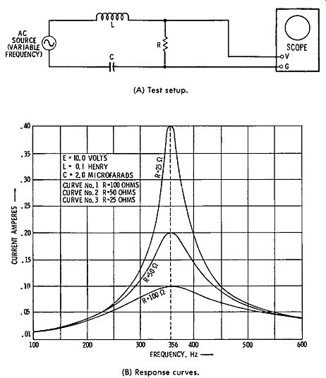
Fig. 5-7. Testing response of LCR series-resonant circuit. (A) Test setup.
(B) Response curves.
TUNED TRANSFORMER
Tuned transformers are used in all transistor radio and TV receivers, and in many other types of electronic equipment.
Tuned-transformer action is based on the resonant response of series and parallel LCR circuits that have mutual inductance.
A series-resonant circuit has frequency-response curves such as those in Fig. 5-7. In this test setup, the scope displays the current variation vs. frequency. The resonant frequency of the circuit is formulated : (5.1)
Since capacitive and inductive reactance cancel at resonance, the current flow is given by: (5.2)
In turn, the bandwidth is given by the number of hertz be tween the -3-dB, or half-power points:
BW = f2 - f1 (5.3)
.... where, f 2 denotes the frequency at the higher half-power point (70.7 percent of maximum voltage point), f1 denotes the frequency at the lower half-power point.
The Q value of the series-resonant circuit is equal to the inductive reactance divided by the resistance of the circuit:
Q = ~L (5.4)
XL = 2 pi fL ( 5.5)
Note that the Q value varies with frequency; at resonance, we write: (5.6)
Qo = X10 (5.7)
The bandwidth of a series-resonant LCR circuit is given to a practical approximation by: BW = _& (5.8)
Qo Observe, also, that R is usually greater than the DC resistance in the circuit, being equal to the rf resistance; Rae in creases with frequency. Therefore, a coil in a series-resonant circuit usually has a maximum Q value at some particular operating frequency.
A parallel-resonant circuit has frequency-response curves such as those in Fig. 5-8. The resonant frequency is given approximately by Formula (5.1). The impedance of a parallel resonant circuit is approximately equal to:
... where, L Z.,=Rc Z0 denotes the impedance at resonance in ohms, L denotes the inductance in henrys, C denotes the capacitance in farads, (5.9) and R denotes the effective ac resistance of the circuit.
(A) Test setup. (B) Response curves.

Fig. 5-8. Testing response of LCR parallel-resonant circuit.
Response curves for inductor current, capacitor current, and capacitor voltage are approximately the same. The generator current has an "upside-down" response curve that is basically similar to the other response curves. In Fig. 5-8, the 20,000 ohm resistor represents the source resistance, such as the collector output resistance of a transistor. At resonance, the circulating current between L and C is equal to Q times the generator current Ig, That is:
Ic =IL= Qig (5.10)
This is called the current amplification of the LCR circuit.
It is analogous to the voltage amplification of a series-resonant circuit; in a series LCR circuit, the generator voltage is stepped up Q times by the inductor and by the capacitor (Fig. 5-7):
Ee= EL= QEg (5.11)
In other words, resonant circuits, in the absence of transistors, can produce either voltage amplification or current amplification, but not both. A transistor can provide voltage amplification and current amplification simultaneously. This is because a transistor is an active device, whereas a resonant circuit is a passive device. There can be no power gain in a passive device.
(A) Tuned transformer. (B) Equivalent circuit. (C) Frequency-response curves for various coefficients of coupling (k).

Fig. 5.9. Bandwidth in two tuned,
coupled circuits.
Tuned transformers (Fig. 5-9) comprise a parallel-resonant circuit and a series-resonant circuit with mutual inductance.
The primary operates as a parallel-resonant circuit; the secondary operates as a series-resonant circuit. Since the primary and secondary are coupled, the series-resonant circuit reflects an impedance into the parallel-resonant circuit that varies with frequency. A preliminary equivalent circuit for a tuned transformer is shown in Fig. 5-9B. If the primary and secondary have the same Q values (as is usually the case}, and are tuned to the same center frequency, the output voltage from the secondary displays frequency-response curves such as shown in Fig. 5-9C. The primary or secondary alone has a ringing waveform in a square-wave test as shown in Fig. 5-10.
A tuned transformer has a ringing waveform such as that illustrated in Fig. 5-11.

Fig. 5-10. Ringing test of primary or secondary of transformer. (A) Test setup.
(B) Waveform. (C) Q equals 107T, or 31.4, in this example.
Note in Fig. 5-9 that the bandwidth of the frequency-response curve depends on the coefficient of coupling. In ordinary tuned transformers, the primary and secondary have the same inductance and the same Q values, and are tuned to the same center frequency. In turn, the maximum possible value of mu tual inductance Lill is formulated:
L = Lp = Ls (5.12)
The coefficient of coupling is the ratio of actual mutual inductance L,n to the value of Lmim•x>:
k= Lill =Lm L11 L, (5.13)
At critical coupling, the frequency-response curve has a single peak. At any greater value of coupling, the response curve has two peaks. The value of critical coupling is formulated: (5.14)
Critical coupling depends on the value of ac resistance. At critical coupling, it can be shown that: (5.15)
It follows from Fig. 5-9B that a tuned transformer has two resonant frequencies, which correspond to the double humps in Fig. 5-9C. That is, the signal current branches in Fig. 5-9B, and the branch currents have different resonant frequencies.
(A) Test setup. (B) Ringing pattern.

Fig. 5-11. Ringing test of tuned transformer.
The hump frequencies are formulated:
fc f11 = V 1 ± k (5.16)
... where, fh denotes the hump frequencies, f0 denotes the center frequency, and k denotes the coefficient of coupling. (The ± signs fork give the two answers.) Since there are two hump frequencies present, these frequencies beat in a square-wave test, as depicted in Fig. 5-12.
If the primary and secondary are tuned to the same center frequency, the beat waveform goes periodically through zero beat, as illustrated in Fig. 5-11. The beat waveform decays exponentially because of the I^2R losses in the primary and secondary. The frequency of the beat envelope is given by Formula (5.16). Therefore, a high-Q tuned transformer has a large number of cycles between zero-beat intervals. The ringing oscillation in Fig. 5-11 is equal to the average of the hump frequencies (it is the center frequency) :
f = f1 + f2 r 2 (5.17)
Since a tuned transformer always has two hump frequencies, the question arises concerning the display of a single peak at critical coupling in Fig. 5-9. The answer is that the two hump frequencies are so close together in this situation that they seem to merge and form a single peak on the scope screen.
(A) Rf input frequency, f,. (C) Beat waveform.
(B) Rf input frequency, f,.

Fig. 5-12. Formation of beat waveform.
IMPEDANCE-COUPLED AMPLIFIERS
Transistor impedance-coupled amplifiers are widely used in TV receivers and other electronic equipment. A simple impedance-coupled amplifier is diagrammed in Fig. 5-1C. The collector load is an impedance, because the inductor has winding resistance; the inductor is also shunted by R1 and the base input resistance of the second transistor. Analysis of this amplifier is basically the same as that of an RC-coupled amplifier, except that the collector load impedance is formulated: (5.18)
... where, Z is the load impedance in ohms, R is the effective resistance in ohms, and XL is the inductive reactance in ohms.
XL= 2 pi fL (5.5)
Fig. 5-13 shows the configuration for a typical transistor video amplifier. This is an impedance-coupled amplifier. The impedance loads comprise inductors (peaking coils) L211, L212, L214, and L213. We call L211 and L212 shunt peaking coils. L213 and L214 are called series peaking coils. These peaking coils provide high-frequency compensation, and flat frequency response from 60 Hz to approximately 3.5 MHz. A video-frequency response curve is illustrated in Fig. 5-14.
Fig. 5-15A shows a simple resistance load, as used in a conventional RC-coupled amplifier. In B, L1 provides shunt peaking. In C, L2 provides series peaking. Of course, series peaking can be used with shunt peaking as in D. It is impractical to design a wide-band amplifier that does not have some form of peaking, because the resistive load must be so small that little gain is obtained. On the other hand, if a shunt peaking coil is used, the load resistor can have a fairly high value, and good gain is obtained over a wide frequency range. If we use series peaking instead of shunt peaking, 50 percent more gain can be obtained. Again, if we use both series and shunt peaking, we can obtain about 80 percent more gain than with shunt peaking alone. In Fig. 5-14, the amplifier is slightly over-compensated, since the response tends to rise at high frequencies.
Fig. 5-16 shows frequency-response curves for various values of shunt peaking. The gain at low frequencies is deter mined by the value of the load resistor. High-frequency gain is determined by the peaking inductance. Note that when the load is resistive only, the frequency response in this example starts to drop off at 700 kHz, but the use of a suitable shunt peaking coil maintains flat response out to 4 MHz. A slight rise occurs at high frequencies. If a peaking coil is used that overcompensates the load, the response is 100 percent at 5.5 MHz, but there is almost 20 percent rise at 4 MHz. This is an excessive amount of frequency distortion.

Fig. 5-13

Fig. 5-14. Video-frequency response curve.
(A) Resistance load-no peaking. (B) Shunt-peaked load. (C) Series-peaked load. (D) Series- and shunt-peaked load.

Fig. 5-15. Puking circuits in RC-coupled amplifier.

Fig. 5-16. Frequency response curves with shunt peaking.
When both series and shunt peaking are used, flat response can be obtained out to 4 MHz with a larger value of load resistor. In turn, higher gain is obtained. When both series and shunt peaking are used, the drop-off is much more abrupt past 4 MHz. This results in poorer square-wave response, because abrupt drop-off is associated with a very nonlinear phase characteristic. In scopes with transistor vertical amplifiers, series peaking only may be utilized, since series peaking produces less overshoot than shunt peaking in square-wave reproduction. A scope that employs both series and shunt peaking has higher gain for a given number of transistors, but in turn has poorer square-wave response. Fig. 5-17 illustrates the 100-kHz square-wave response of a series- and shunt-peaked video amplifier in a color-TV receiver that has a phase-equalizing circuit to develop symmetrical square-wave response. Overshoot and preshoot are approximately equal in this arrangement.

Fig. 5-17. Preshoot and overshoot in the 100-kHz square-wave response of a
color TV video amplifier.
DIRECT-COUPLED AMPLIFIERS
Direct-coupled amplifiers are extensively used in transistor equipment. A basic direct-coupled amplifier is shown in Fig. 5-1D. This type of amplifier is used for amplification of DC signals and very-low-frequency signals, as well as high frequency signals. Direct-coupled amplifiers are attractive be cause they dispense with coupling capacitors or transformers.
On the other hand, temperature stabilization is a greater problem than in ac coupled amplifiers. Various circuit means are utilized to avoid DC drift. In the foregoing circuit, an npn transistor is connected directly to a pnp transistor. Thereby, bias polarities are correctly provided. If the collector current in the first stage is greater than the base current in the second stage, a collector load resistor R1 must be included.
Fig. 5-18 depicts a three-stage direct-coupled amplifier. Npn transistors are used, and are forward-biased for class-A operation by means of a voltage-divider network. To provide good bias stabilization, R7 operates as a negative-feedback emitter resistor in the output stage. In addition, DC feedback is pro vided from the emitter of Q3 to the base of Q1 via R6. Suppose that the base bias on Q1 tends to drift more positive; in turn, the base bias on Q2 becomes less positive, as does the base bias on Q3. Therefore less emitter current is drawn by Q3, and its emitter voltage becomes less positive. Accordingly, the base bias on Q1 is prevented from drifting via feedback through R6.

Fig. 5-18, Three-stage direct-coupled amplifier.
Q1 in Fig. 5-18 operates in the CE configuration, as does Q3. Q2 operates as an emitter follower. Additional bias stabilization is provided in the emitter circuit of Q2; R7 and the base-emitter junction resistance of Q3 serve as a current feedback emitter resistance for Q2. Q2 also serves as an electronic impedance-matching device between Q1 and Q3, since the collector-output resistance of Q1 is high, and the base input resistance of Q3 is comparatively low. Transformer coupling is used between Q3 and the speakers to obtain a good impedance match. Since the frequency response of a direct coupled amplifier is very good, the system in Fig. 5-18 has a frequency response that is basically the response of TL Square-wave response also is chiefly determined by the characteristics of T1.
QUIZ
1. What is the theoretical maximum available gain of a trans former-coupled amplifier?
2. State an advantage and a disadvantage of transformer coupling.
3. Define leakage reactance.
4. Why does an output transformer not have a rising frequency response?
5. How does a rising frequency response affect square-wave reproduction?
6. Describe crossover distortion as displayed on a scope screen.
7. How is crossover distortion minimized in a push-pull amplifier?
8. Explain how the Q of a coil affects the bandwidth of an LCR resonant circuit.
9. Define the voltage amplification of a series-resonant LCR circuit.
10. Define the current amplification of a parallel-resonant LCR circuit.
11. Describe what is meant by the coupling coefficient of a tuned transformer.
12. Define critical coupling.
13. Explain how the hump frequencies of an overcoupled transformer are calculated.
14. Discuss the characteristics of an impedance-coupled amplifier.
15. How is series peaking distinguished from shunt peaking?
16. With other things being equal, does series or shunt peaking provide higher gain
17. Compare the gain provided by series-shunt peaking with that of shunt peaking alone.
18. How do peaking coils affect the square-wave response of an amplifier?
19. Why is a slight rise at high frequencies often tolerated in a video amplifier?
20. What is the disadvantage of substantial over-peaking?
21. Describe the general features of a direct-coupled amplifier.
22. What is the basic problem that must be contended with in direct-coupled configurations?
23. Name an advantage of a direct-coupled amplifier.
24. How can bias stabilization be obtained in a direct-coupled amplifier?