SWITCHED POWER
I READ WITH INTEREST Randolph Vikan's article (TAA 4/88, Part 1). I wondered when someone would offer a car amplifier in TAA. The DC-DC converter is an important part of the project and is technologically the most difficult part of the design. The design and description of its operation show that Mr. Vikan does not have an understanding of how switch-mode power supplies work. I design switching and linear power sup plies for a living and I hope the following will be useful.
The principle used in switching power supplies is that of averaging. In a fixed frequency pulse-width modulation (PWM) system, the volt-second product (the length of time the switches are turned on times the input voltage) is always adjusted to be a constant. The power supply needs this to keep the output voltage constant. If the input voltage goes up, the conduction time of the switches will be reduced to keep the volt-second product constant. This action produces a pulse train of varying height and duty cycle, but which has a constant average value.
If the pulse train is input to an LC filter with a cutoff frequency which is much lower than the switching frequency, the filter's output essentially will be DC and will have a constant value since the input pulse train had a constant volt second product.
If the inductor in the output filter is eliminated, the output capacitor will peak charge to the input voltage and all PWM regulation will be lost.
A DC-DC transformer is similar to a switch-mode power supply but it does not provide regulation. The switching transistors are driven at the maximum duty factor at all times and the output filter is a simple capacitor.
Some problems arise when trying to pulse-width modulate a DC-DC transformer. I expect your circuit will have these problems. The length of time each pair of transistors is conducting can vary slightly. A continuous difference of as little as 0.lusec can cause complete saturation of the transformer. This results in large current spikes in the switching transistors and your circuit has no mechanism to limit the current.
This also will occur with DC-DC transformers.
PWM in your circuit will result in reasonably long periods of time when the transistors are not conducting and all the output current is supplied by the output capacitors. These capacitors will discharge by a few hundred millivolts.
When the next transistor pair turns on, he voltage at the output of the rectifiers will be higher than the voltage across he output capacitors. Since there is very little impedance between these two voltages, a high current spike will result n both the transistors and the capacitors, which is detrimental.
Since your design does not include an output inductor, regulation of the output voltage in the classic PWM sense is not possible. I suspect your circuit normally operates with very narrow output pulses. Higher reliability, lower noise and lower output impedance are all possible with an output inductor.
PHILIP C. TODD Scottsdale, AZ 85260 USA.
Randolph Vikan replies:
With Mr. Todd's analysis, I realize I need to clarify some of my design decisions for TAA readers.
My article was intended as a description of the construction and operation of my power supply, not a dissertation on switching power supplies in general.
I assumed if anyone was interested in a broader coverage of the field, they would refer to my references at the end of Part I (1 and 6).
Vout =Vin Ton/T
Ton /T CONTROL LOOP
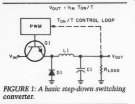
FIGURE 1: A basic step-down switching converter.
The circuit Mr. Todd describes is a basic step-down switching converter (Fig. 1). The average (DC) value of the pulse train coming from the switch (Q1) is Vout = Via Tul/T; where Tea is the switch-closed time and T is the switching period (Pressman, p. 5). In this circuit, L1 and C1 reduce the ripple component (Via peak-to-peak) to an acceptable level. To make this circuit a voltage regulator, a negative feedback loop (dot ted line) is added to monitor the output voltage (Vow). The T./T ratio (duty cycle) of the pulse train is varied to provide voltage regulation.

FIGURE 2: A half-cycle, width-modulated converter regulator.
My PWM power supply is a variation on the traditional push-pull converter called a half-cycle, width modulated converter regulator (see Fig. 2, Press man, pp. 68-72). The output voltage of this circuit can be set, by varying the Ton/(T/2) ratio, to any value less than (Vin - Viat)(Ns/Np) - Va; where Vig: is the saturation voltage of the switchers and Va is the forward drop of the rectifiers.
The output inductor L2 and capacitor C2 function to smooth the square wave coming from the rectifier diodes. The inductor is not absolutely required for regulation, that function is handled by the feedback loop that controls the Ton/(T/2) ratio.
I chose to leave the inductors out of my supply to simplify the construction.
It's difficult enough to wind one trans former, let alone the four more custom made inductors that would be required, one for each rail. Also the two inductors required on the + 36V DC rails must be physically as large as the main trans former to be effective. Commercial car amps that use this type of regulation often make this compromise, too. The price we pay is a slightly noisier output and the higher than usual current spikes Mr. Todd describes. Heavy-duty components and large filter capacitors help to minimize any effects on reliability these spikes may have.
Mr. Todd also mentions the possibility of saturation of the transformer due to continuous imbalances in its primary circuit. This can be a problem with push-pull converters, especially ones that operate at high voltages, such as off line switchers. If the switching and saturation characteristics of the switching devices are different on a continuous basis, the core can go into saturation due to a process called 'flux walking.’ As the core saturates, it takes greater and greater current to magnetize it. If the core saturates during the part of a half cycle when the switching device still has drive, the device may be destroyed by exceeding its SOA or its dissipation limits. But small initial imbalances can be tolerated and will be automatically equalized by the core ‘walking’ toward saturation. As saturation is approached, the larger current in the transistor producing the larger volt-second area results in larger Vi.esar (saturation voltage between collector and emitter), or Visgsan with MOSFETs; subsequently less volt second area is applied to that half win ding. This causes the core to cease ‘walking ’ before a disastrous condition exists (Pressman, p. 267). The use of MOSFETs as switchers can prevent core saturation problems since their Vaseay is proportional to the current going through them, which helps to equalize volt-second area if imbalances occur.
I could have installed a complex symmetry-correction circuit in my design, requiring even more custom magnetic components, but I don't believe it's necessary since I have not experienced core saturation problems in my proto types. In fact I've not experienced any power supply failures in any of my three amps, one of which has been operating in my car for three years.
The circuit values I'm using in my PWM supply do produce somewhat narrow duty-cycle pulses, when the power supply is not called on to deliver much current; idling, my stereo amps draw 200mA from the 36V DC rails and 50mA from the +45V DC rails. When neither of the switching MOSFETs are on, the filter capacitors C9-C12 provide all the current to the load. When current demands increase, so does the length of the duty cycle to meet these demands.
I recently modified my stock design slightly to create wider switching pulses during normal (idle) operation and allow the use of 35V capacitors for C10 and C11. This is not mandatory, since the original design operates just fine. I decided to make this mod based on ease of transformer winding and the slight improvement larger capacitors will make in the supply's performance.
Simply reduce the transformer's secondary turns from 15 to 11 and the tertiary turns from 4 to 3. Change resistor R16 to 36k and change C10 and C11 to 3,300uF/35V DC capacitors, such as Sprague 80D #332PO35KAS. The supply voltages will be +33V DC and +43V DC, and the duty cycle of each switcher will be about 20%. The voltage at pin 9 of IC1 will be approximately + 1.5V DC at idle.
In conclusion, Mr. Todd has kindly offered to do a paper design of a switching power supply for the benefit of TAA readers. I'm sure many readers would like to see it; unfortunately he hasn't the time to build an actual working model.
If Mr. Todd took the time to fully con struct his design, we could actually compare performance. We could also benefit from a TAA construction article with an explanation of operation, construction hints and a parts list. To implement a paper design, many need some kind of kit that includes circuit boards and parts. Without these, a paper design is only so much paper.
14-BIT CORRECTIONS
TWO ERRORS IN MY article ‘Greening Magnavox 14-Bit CDs, ’ (TAA 4/88) have come to my attention. First, for the 1uF capacitor, the Panasonic P-Series does not offer a value that large. Thanks to Lipford Moy of Greenville, MS for noting this. Table 1 lists alternate caps and sources. Use one of these or a personal favorite.
The second error is more serious. On the Piggyback #2 artwork (Fig. 4a, p. 22), the servo amp on the right channel has the input and output resistors going to the wrong pins of U5. The schematic and stuffing guide are correct. If you al ready etched a board, follow my re worked drawings in Fig. 1. Figure 2 is the correct circuit pattern. I'm sorry for any inconvenience this might have caused.
--------------
-------------
TABLE 1 --- 1 uF SOURCES
Mfg. | Part Number
Panasonic Mepco-Centr.
ECQ-E1105KZ MP 719A1AD105PK630SH MP1 719B1GG105PK101SB MPCt 105MPR250K MPP 105MSR100K MP MP: Metal-polyester MPP: Metal-polypropylene MPC: Metal-polycarbonate
* Digi-Key t Hamiiton-Avent
** Caulder Elect. (800) 632-2805 Illinois Cap
-----------------
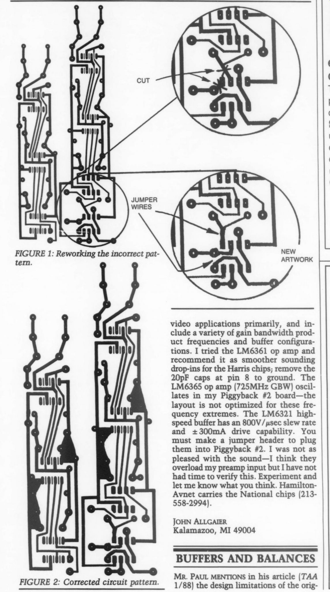
FIGURE 1: Reworking the incorrect pattern.
FIGURE 2: Corrected circuit pattern.
---------------
Since choosing the Harris HA2520 op amps, National has come out with a new VIP series. These are intended for video applications primarily, and include a variety of gain bandwidth product frequencies and buffer configurations. I tried the LM6361 op amp and recommend it as smoother sounding drop-ins for the Harris chips; remove the 20pF caps at pin 8 to ground. The LM6365 op amp (725MHz GBW) oscillates in my Piggyback #2 board-the layout is not optimized for these frequency extremes. The LM6321 high speed buffer has an 800V/u-sec slew rate and +300mA drive capability. You must make a jumper header to plug them into Piggyback #2. I was not as pleased with the sound-I think they overload my preamp input but I have not had time to verify this. Experiment and let me know what you think. Hamilton Avnet carries the National chips (213 558-2994).
JOHN ALLGAIER Kalamazoo, MI 49004
BUFFERS AND BALANCES
------------------
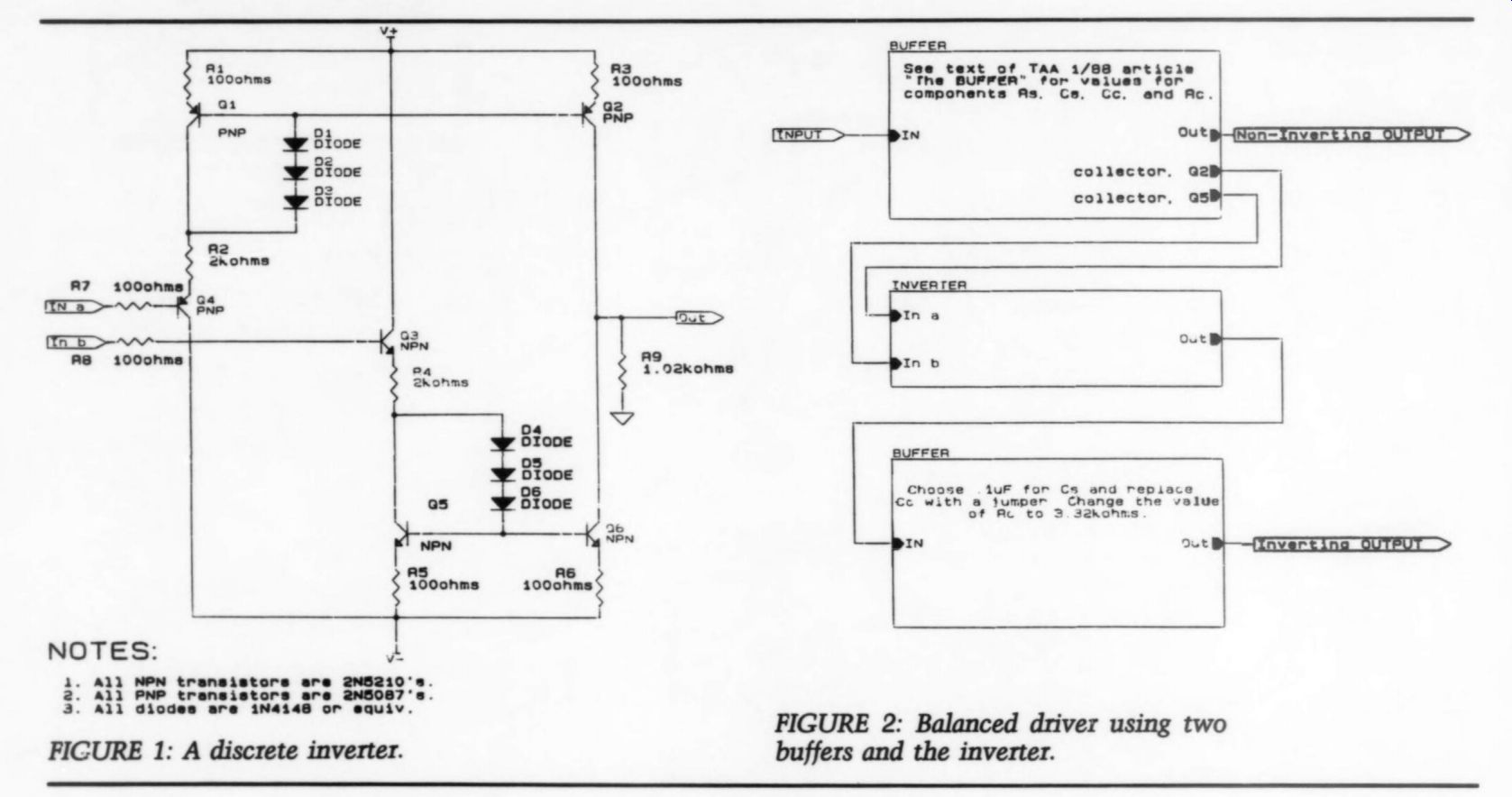
FIGURE 1: A discrete inverter. NOTES: 1. All NPN transistors are 2N8S210. 2. All PNP transistors are 2N8087. 3. All diodes are 1IN4148 or equiv.
FIGURE 2: Balanced driver using two buffers and the inverter.
-------------
MR. PAUL MENTIONS in his article (TAA 1/88) the design limitations of the original super buffer. I have been using this circuit as a balanced out-line driver into 30 feet of cable to my Pro Crown amp.
I would like to replace the circuit with Mr. Paul's buffer. Is it possible to change this to an inverting buffer for the negative half of the balanced line driver? This would avoid using an op amp in the inverting mode and slow down the buffer's speed.
If his circuit cannot be changed, Burr Brown has an op amp combo that would work for an inverting high-speed buffer amp. The OPA606 is buffered with OPA633 in the inverting mode. The 633 slew rate is 1000V/ u-sec and is defined as a video/ current buffer. The 606 is a FET (35V/ usec) used in the feedback loop in the inverting mode. Another candidate for the OPA606 is PMI OP-44 (100V/ u-sec/AVcl 3) and the OP-42 for unity gain (50V/pusec). The best possibility is the OP-42 in the feedback loop inverting mode with your buffer. Would it work?
ASHBY
Box Fort Lauderdale, FL 33317
Chris Paul replies: Before we discuss a design, let's talk about balanced and unbalanced drivers and receivers.
A balanced interface (two signals 180 degrees out of phase) is preferable to an unbalanced interface (one ground referenced signal). First, even a shielded cable cannot fully prevent ambient electromagnetic signals such as power line 'hum' or radio frequencies from being impressed upon signal leads inside the cable. In an unbalanced (single-ended) interface, these interfering signals cannot be distinguished from, and are therefore added to, the desired signal. In a balanced interface, the two lines inside the cable are also susceptible to interference pick up. Since these two lines are physically very close and ideally have identical impedances, identical interference signals are impressed upon both lines. However, the balanced receiver looks at the difference between the signals, and the interference is canceled.
With a balanced interface, drivers and receivers also can be virtually independent of signal ground. This can be a great asset in isolating signals from the heavy ground currents which might otherwise flow in unbalanced outputs.
Whether you choose to design balanced drivers with tubes, op amps or discrete semiconductors, the two drivers should be electrically identical so the impedances of the lines they drive are identical, for the reasons I mentioned. I there fore do not recommend a design mixing the OPA633 and my buffer. Second, the input of the inverting driver should never be taken from the output of the noninverting driver. Following this rule pre vents interference on the noninverting line from getting into the inverting driver. Although you might infer that the inverting and noninverting driver inputs should be driven from the same point, this can create other problems because the input impedance of an inverting op amp or discrete stage can be fairly low.
By driving an inverter stage from the middle of a buffer stage, you avoid both problems.
A discrete inverter is shown in Fig. 1.
The inverter inputs are driven from the Q2 and Q5 collectors of my buffer. The inverter's Q3 and Q4 drive current mirrors through R4 and R2. One current mirror consists of transistors Q5 and Q6 and resistors R5 and R6. The other consists of Q1, Q2 and R1, R3. The diode strings allow Q1 and QS5 to operate at higher collector-base reverse bias voltages, resulting in more linear operation. The current mirrors terminate in resistor R9. A value of 1k for R9 would have resulted in a unity gain inverter. The slightly larger value of 1.02k compensates for the input load presented by the modified buffer driven by the inverter.
The inverter shares many specifications of the buffer. Bandwidth is in the 10s of MHz, and slew rate is several hundred volts per microsecond. THD is more than 70dB down at 5V RMS, dropping to about 80dB down (.01%) at 2V RMS. The output impedance is a moderate 1kf2, but the inverter was not designed to directly drive a line, but rather a buffer, and 1 k-O is more than adequate. The inverter topology does not afford much in the way of PSRR, and I recommend a well-regulated power supply.
Figure 2 shows how to connect two buffers and an inverter to create a balanced line driver. The buffer driving the noninverting leg also drives the inverter from the collectors of its Q2 and Q5 and can be configured to any of the options mentioned in the original article. (Again, to attain adequate filtering of infrasonic grunge, I suggest at least a second-order type.) The buffer in the inverting leg, however, should produce a signal that is as close to an exact inversion of that driving the noninverting buffer as possible.
Here we opt for DC-coupling by replacing Cc with a jumper, since the driving signal has already been infrasonically filtered, courtesy of the noninverting buffer. To be certain the inverting buffer's op amp servo can cancel any DC offset, we reduce the value of Rc.
MORE POWER TO MOSFET
WILLIAM CHATER'S MOSFET amp looks very innovative. I'm impressed with its overload handling and design.
I wonder whether Mr. Chater might publish the component changes neces sary to create a more powerful version? Using today's quality speaker drivers, with efficiency in the ballpark of 91dB 1W/m and power handling of 1,000W, the Chater amplifier can only deliver a SPL of approximately 107dB with a maximum transient SPL of 110dB. I wish to build a 200W version to be able to handle the increased dynamics of today's best CDs.
Will Richard Marsh's circuit board for his high quality dual tracking voltage regulator be offered by Old Colony? WILL FIRSTBROOK Oakville, Ontario L6L 3B3 Canada
Bill Chater replies:
Mr. Firstbrook is not the first to request a higher power version of my MOSFET power amp. It is a fact of life, as he correctly describes, that some loudspeakers' efficiency dictates the use of a higher power amplifier than 40W.
I deliberately selected the modest power level to demonstrate how the con trolled-clipping feature could benefit the sound of an amplifier. To apply the technique to a much higher power level would not have as graphically demonstrated the point.
Unfortunately, it is not just a matter of a few component changes for an increase in power. My closing remarks in the second part of the article address this point; in addition, the driver stages would require some modification which includes raising their operating points, as well as other factors.
I suggest that Mr. Firstbrook consider using a biamp arrangement using the 40W amplifier to provide the high frequency channels. This would afford a power reserve not available with a single amplifier covering the whole frequency range. He could then use a duplicate set of the present design for the low-frequency channels, or a different amplifier of higher rating.
HOT PAS
I ADDED THE FILAMENT voltage regulator to my modified PAS as outlined in Pat Amer's letter (TAA 4/87). It worked fine at first, but after an hour or so I noticed the distinctive smell of burning trans former insulation. Lo and behold, my stock PAS transformer was hotter than h__ _! Then I looked at the circuit carefully and realized that connecting all four filaments in parallel forces the trans former to supply approximately twice as much current as it did previously.
The only way to provide the juice needed is to add a separate filament transformer, with a higher current rating.
I used a 12.6V transformer and eliminated the 100 resistor and it's been working fine ever since.
I bring this problem to your attention in the unlikely event no one else has.
On another note, TAA has published several fine vacuum tube construction circuits; unfortunately, no articles (since W.Z. Johnson, 4/77) on building or modifying tube power amps. I realize obtaining the output transformers is difficult, but I'm building an amp from scratch right now using ‘previously owned ’ transformers. How about it? Thank you for an excellent magazine.
Keep up the good work!
MARK Huss W. Collingswood, NJ 08107
Pat Amer replies:
Mr. Huss is correct that the heater regulator circuit I recommended (TAA 4/87, p- 50) calls upon the transformer to de Liver about twice as much current, about 600mA, as previously. I have built two Auroras with this circuit, and the trans formers in both cases get warm under load, but supply the current without trouble, even in an always-on mode.
Dynaco supplied many different transformers, however, over the life of the PAS-2 and PAS-3. Some transformers, it seems, cannot supply 600mA to the heater circuit without overheating. If your transformer becomes too hot to touch, or if the insulation begins to burn, it can't take the load, and you need a separate transformer if you wish to use my circuit. I would recommend a trans former which will supply 16V or more into a 600mA load so you can use the regulator. If you decide not to use the regulator, you might as well go back to the original Dynaco series-parallel circuit, which the transformer can supply.
TTT QUERY
HAVING PREVIOUSLY written an article on solid-state relays and a sequencer, may I offer congratulations to Mr. Nitikman on his sequenced on/off switch (TAA 2/88). My first reaction was, ‘Why didn't I think of that. ’ However, I wish to offer some comment on the circuit and the text. I think the author should have fully explained the Schmitt trigger IC, which is simply an inverter with hysteresis input, that is, a gap in the turn on/off input, which is about 0.4V.
In addition, the ICs covered are evidently Motorola units (MC14584 and MC14194), also available from Jameco (74C14 and 74C194). Now, as these devices are CMOS, they can operate at a much higher voltage, which would give a better noise margin. I breadboarded Mr. Nitikman's circuit and used a 12V regulator, which is fine with the same transformer and filter cap. However, you need to add series resistors if LEDs are used.
One more item: Mr. Nitikman should have explained that the Schmitt trigger IC is a 14-pin unit, so the circuit board layout actually uses what appears to be pins 8 and 9 for a strap, and the IC should be in the holes nearest the edge of the board, as Fig. 2 shows.
L.B. DALZELL El Cajon, CA 92020
Steven Nitikman replies: Thank you for your letter and interest in my design. I thoroughly enjoyed your related article, ‘Using Solid-State Relays: Safe Power Control,’ (TAA 2/86).
The function of the hex Schmitt inverter package is necessary to my circuit.
A regular hex inverter will not function properly in the sequencer. Two inverters must be Schmitt devices; they make up pins 5, 6 and pins 12, 13.
Using a 5V supply, a positive step in put of 2.9V will cause this inverter's output to change states (go low) and a negative step input of 2.3V will cause it to go high. This gives us a noise immunity of 0.6V (2.9 - 2.3). With higher supply volt ages, noise immunity is appreciably better.
Referring to the schematic diagram: R1; C3 inverter, pins 5 and 6; and SW1 make up a bounce-free switch. R1 and C3 slow down SW1 ’s response time to remove contact bounce inherent in all mechanical switches while the inverter delivers a clean step to pin 6 in response to the slowly changing input.
The oscillator which clocks the shift regulator uses pins 12 and 13 of the inverter package. Operation is as follows: assume that pin 12 (output) is low. Since the device is an inverter, pin 13 (input) must be high. However, pin 12 is discharging C4 through R3. When C4 drops to around 2.3V, the inverter sees a logic low on its input and pin 12 now goes high. C4 is now charging through R3 and when C4 reaches 2.9V, pin 12 goes low and the whole cycle keeps repeating.
This is an ultra simple, noncritical oscillator which only works with Schmitt input devices.
As you guessed, I had Motorola devices in mind when I developed the circuit. I had hoped showing a 4000 series number in the Parts List would be sufficient. The 4584 is second-sourced by other manufacturers; Motorola may be the only sup plier of the 4194 as the MC1494BCP.
Your device alternatives will no doubt work well in the circuit.
When I designed the circuit, I fully realized that higher supply voltages offer better noise immunity with standard CMOS logic. I chose 5V operation be cause solid-state relay RY 1 carries a maximum rated input of only 8V. Also, with a 5V supply, standard buffered CMOS can directly drive LEDs without the need for the usual current limiting resistors.
On occasion, I have come across large solid-state relays (as used for RY2) rated at 5V on the inputs. CMOS 4000 series integrated circuits feature excellent noise immunity, even at 5V and in view of the extremely low switching speeds characteristic of my circuit, as well as its simplicity, performance will not suffer.
I have built four working prototypes without running into problems. Standard CMOS operating at 5V has no problem driving solid-state relays.
I regret that the placement of IC1 may be confusing for readers. Since the stuffing guide clearly shows the position of the jumper, I assumed no problems would result. Thank you for clarifying this in TAA.
For excellent reading on practical CMOS, Don Lancaster's ‘CMOS Cook book ’ (Sams 21398, available from Old Colony Sound Lab, $14.95) is a must. I believe it is still the best book ever writ ten on using real world CMOS.
POOGE-4 CIRCUITS
I AM INSTALLING Mr. Jung's POOGE-4 circuits in my Magnavox CD player.
These will replace his Audio circuits which I installed several months ago.
Why didn't Mr. Jung use an NE5302/ LH00002 pair in the I/V converter?
After Fo < the problems with op amp proven. #5. Aa cme nd he then failed to use one in this application.
MICHAEL HALBROOK
Houston, TX 77231
Walt Jung replies:
The amplifier circuits were laid out for a small board, and contain three 8-pin DIP footprints. The overall outline for this board must be electrically plug-replaceable and fit in all players without interference, to satisfy our common-de nominator kit criterion. So, there are limits to how much circuitry you can cram on this card. If you are building just one mod for yourself and have lots of time, feel free to try a buffer for the I/V stage as well, such as the ‘0002 ’ circuit.
It helps here as well, even though we have found the line driver stage to be an even more dramatic upgrade.
As you may by now realize, POOGE-4 is not just a collection of useful circuit upgrades, they are also carefully chosen to yield maximum performance for the effort spent. Good luck with your own POOGE-4, let us know of your variations, and how it all fares in the end.
CD RATINGS
I AGREE WITH MR. Kelly's comments ( ‘Letters,’ TAA 2/87, p. 54) about the usefulness of a CD sonic rating checklist.
While I do not think that TAA should publish reviews on the musical aspects of recordings, a quality scorecard would be highly useful, indeed.
I suggest a reader reply card could be used, with space for maybe a dozen CD titles to be entered, and rated numerically, for example, from zero to seven. You could also leave space for comments, such as 'one track has lots of hiss,' and SO on.
Regarding Barbara Streisand's Broad way Album, 1 am afraid Mr. Kelly is suffering from a defective player, rather than a substandard recording. I have listened to it not only on my system, but while auditioning expensive equipment at a number of high-end audio dealers. In no case did it show anything other than outstanding dynamics.
For pop music, I am surprised that the majors are now making high quality CDs, while the traditional small labels, such as Rounder, are often content to give us unlistenable sonic garbage. The audiophile small labels (Reference Recordings, DMP) are typically top-notch.
I am still chagrined, by the way, that your neighbor, Wayne Green, is content to pitch his magazine at the lowest common denominator (but at least they now listen to the disc before reviewing it). Hi Fi News & Record Review, on the other hand, while a paragon of enlightened technical wisdom, seems to have Martians writing their pop music reviews.
Returning to CD players, based on CAL Tempest versus Linn, Mission versus Sota, and similar auditions I made, there still seems to be some improved solidity and three-dimensionality for LPs over CDs. For most of us though, good sound from a CD is much more afford able than from a top-line analog setup.
I have been working with Dave Berning trying to beat my Sony CDP 52011 in to shape, and comparing it to his prototype Philips, with tubes, machine. In stock form the Sony was trounced. By doing op amp swaps and replacing the output cap with a servo loop we have been able to eliminate all the transitory tizziness. The tube unit still has a better soundstage and rounder solidity, but the units are close. I have not yet tried power supply modifications.
VYTENIS BABRAUSKAS
Bethesda, MD 20814
PUSH-PULL DATA
IS ANY PERFORMANCE DATA available for Mr. Marsh's push-pull shunt regulator (TAA 1/88)? I would be most interested in seeing it, if possible.
A.J. STEEN
Los Angeles, CA 90025 Mr. Marsh replies:
I used to have some test results, but they are lost in moving, or buried in boxes stored in my garage. Most tests were done for me by Joe Norris, a wonderful man who used to work for the David Hafler Co. To some extent, how well it measures would depend on your choice of pre-regulator circuit. I primarily wrote the article to spur new ideas and designs.
Already, some good improvements and ideas have come forth. Perhaps a new trend will develop out of it.
I would be interested in any work and results you or others have been doing, also. Sharing information benefits everyone.
-------------------
Also see:
TEST REPORT, By Hampton Childress