MEASURING NONLINEAR DISTORTIONS, Part 3
BY ERNO BORBELY
IN THE FIRST PART (TAA 2/89) of this series on my multi-tone intermodulation meter, we looked at the different sources of nonlinear distortions and their measurement. In Part II (TAA 3/89) 1 presented the IM meter, with which you can carry out four different types of IM measurement. In those articles I promised to apply these measurements to existing amplifiers and pro pose improvements. So here we will be investigating new topologies that arise when such measurements can result in better/or less expensive designs.
The IM meter has indeed been used a lot in testing the basic topologies that you already know from my previous de signs. This resulted first of all in general improvements in linearity, but also triggered some significant changes which can easily be classified as new.
I hasten to add here that the changes might in themselves not represent new circuit design ideas, nor are they necessarily my ideas. In fact, I have deliberately tried to collect the best there is, or the best that I know of, in current audio design. I firmly believe that you will be treated to details of circuit designs which you can only see in the best audio amplifiers today. I will try to give the customary credit when credit is due. In case I fail to do so and
ABOUT THE AUTHOR: Emo Borbely is currently employed by National Semiconductor as its training manager for Europe. He received a degree in electronic engineering from the Technical University of Norway in 1961 and worked for the ing professional audio equipment for seven years. He lived in the US and was director of engineering for Dynaco and The David Hafler Company. From 1973-78 he worked for Motorola Geneva, Switzerland, as senior applications engineer.
“RHEIN INNER you know the source, please let me know and I will correct it.
A Note About Feedback: Before I embark on the process of dissecting amplifiers, I would like to comment generally on feedback and more specifically on open-loop gain, open-loop bandwidth, feedback factor, and stability. But first a bit of history: when feedback was first used by Black back in 1927, its sole purpose was to linearize the characteristics of the active devices (tubes) used in long-distance telephone repeaters. Stability was hardly an issue at that time; slow de vices and low gain automatically pre vented such problems. Later, with the introduction of faster tubes and the more sophisticated application of feed back (for example, for stabilizing DC and AC gain, manipulating input and output impedances, ensuring long term reliability, and so forth), stability be came an issue and received plenty of attention.
History repeated itself with the introduction of transistors. The first ones being slow and expensive, were used sparingly and consequently it was easy to take care of stability. As transistors became less expensive while designers still lacked the expertise to design inherently linear circuits, we used the easy way out: we added more stages to get a higher open-loop gain and then added global feedback to cure the linearity problems. This soon produced triple-O-type distortion figures at low frequencies, but severe problems often accompanied high ones. Because of the slow output devices at that time, we had to roll off the open-loop bandwidth rather early in order to preserve stability. This resulted in decreasing feed back factor, and the benefit of feedback in curing the linearity problems at high frequencies was gone.
An increasing THD at higher frequencies is, in itself, not a big problem; after all, very few people can hear harmonics of much higher than 10kHz.
But if the nonlinearities also cause intermodulation products which fold back into the audio range and are not masked by other sounds, then the sound quality suffers. Additionally, amplifiers of this period also suffered from slew-related distortion, most from sub slewing. Some of them were so slow that they went into plain slew limiting, causing one of the well-known forms of dynamic distortion: TIM. This has led to the reinvention of feedback amplifier design, with the well-known statement that the open-loop band width of the amplifier has to be equal to or larger than the highest audio frequency, i.e., 20kHz. Although we know that as long as you bandlimit your audio signal to less than the open loop bandwidth of the amplifier there will be no overshoot and no TIM, amplifiers with open-loop bandwidth of less than 20kHz don't have to suffer from TIM either, if the slew rate is high enough.! Now, an amplifier with high open-loop gain and correspondingly lower open-loop bandwidth is equivalent in terms of slew rate to an amplifier with lower open-loop gain and higher open-loop bandwidth, as long as the gain crossover frequency is the same. And as long as the slew rate of the amplifier is high enough, there will be no TIM and you can use the benefits of feedback to make your amplifier more reliable.
Mind you, I am not lobbying for high open-loop gain and high feedback factor--I am advocating good linearity. Good linearity starts with good open-loop linearity, and it should be good across the whole audio range. Personally, I put more emphasis on the high end of the audio range, because this is where nonlinearity produces in-band inter modulation products.
Adding feedback to an already linear system is like putting the icing on the cake. At low and mid frequencies a high feedback factor reduces not only the THD, but also the intermodulation products caused by high frequency non linearities. Ideally, you should combine good wideband open-loop linearity with wide open-loop bandwidth, so that the feedback will also reduce the high frequency nonlinearities which produce the in-band intermodulation products in the first place. Generally, I try to design my amplifiers with this in mind.
However, in many cases the high open loop gain, high feedback factor seems to give the best overall results. In the following exercises I will give you some insight into my own design methodology, in hope that you will then be able to make better decisions for yourself about the application of feedback.
The Line-amp
To illustrate the process of dissecting a circuit and improving its linearity, I started with my lineamp from the Borbely Preamp (TAA 1/86, p. 19). Its basic topology has also been used in the RIAA-2 section, the 60W power amp, and the Servo 100 and DC 100 power amps. I have made a couple of modifications to the lineamp since it was published; the major one was the re placement of the output transistors by MOSFETs. I have also abandoned the active balance control, partly because of availability problems with the pots, but also because some of its users claimed that the control influenced the sound field. Although I have never managed to verify this claim myself, I changed to passive balance nevertheless.
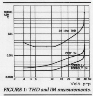
The first measurement I carried out was on the original circuit with bipolar output transistors and with the balance control replaced by a 2500 resistor. The 20kHz THD and the IM measurements are shown in Fig. 1. Considering the scale of the distortions measured, I would say it is quite respectable. Up to about 3V RMS the distortions are below the threshold of the sensitivity of my equipment, and above approximately 4V RMS they increase monotonically.
Since I only need about 1.5VRMS to drive my power amps to full power, this seems to be more than adequate for my purpose. However, nobody would deny that this amplifier has nonlinearities. The purpose of the following exercise then, is to improve the linearity of this circuit.
Looking at the schematic of the line amp you soon realize that all stages contribute to its nonlinearity. Starting with the output stage, I replaced the bipolars with MOSFETs for two reasons: drive capability and sound. I wanted to be able to drive 600-ohm loads (which I use in special applications) and I have found that the MOSFETs sound cleaner and more open. Yet when measuring the amp with MOSFETs there is very little improvement in the 20kHz THD-only the IM measurements show some decrease. At this time I also tried a number of different transistors for the second stage, since I knew from my previous designs that this is one of the most critical elements in an amplifier with this topology.
Although I managed to get some improvements with other transistors, it was soon clear that the output stage was causing most of the nonlinearity.
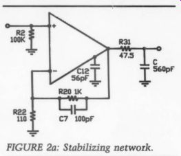
FIGURE 2b: Distortion measurements.
This was also confirmed with the next change I made.
Generally speaking, I have had very good experience with the NPD5566/ AH5020CJN- and P-channel J-FETSs (notably as the input follower in the DC 100 power amplifier), but strictly speaking they are not complementary devices. As I got more and more involved with the Toshiba JFETs, I found that the 2SK240/2SJ75 dual devices would be good candidates for the input stage, but I didn't have samples of these at the time I wrote the article. They are matched devices in a common metal case, similar to the 2SK146/2SJ73 ones used in my MC preamp, but with approximately half the transconductance (gm = 22 mmbho). Toshiba also makes monolithic duals: the 2SK389/2SJ109 with practically the same characteristics as the 2SK240/2SJ75. These monolithic duals were brought to my attention by Mr. Driscoll from Australia, and in the meantime I have been using both dual-types in a number of new designs.
(I have had letters from readers saying that the 25K240/2SJ75 devices are no longer made, however my supplier in Japan says that they are available. In deed, I have just ordered a larger quantity of both dual-types to stock them for present and future designs.) In replacing the NPD/AH with the 2SK240/28]75 pair I also changed the input current from 5SmA per transistor to 2mA. You can do this without in creasing the input noise because the Toshibas have lower noise than the NPD/AH. The reason for this change has something to do with the current sources, as you will see later. To accommodate the change in input cur rent, I changed resistors R9, R10 to 1.27k, and drain resistors R4, R15 to 1.4k, R5, R16 to 402. I also optimized …
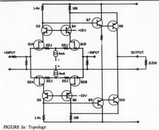
FIGURE 3a: Topology.
… capacitors C3, C5 to 100 pF for the best square wave, as well as reworked the rest of the stabilizing network of the amp as shown in Fig. 2a. Note the RC network at the output of the amplifier, which is now part of the stability net work. The amplifier, stabilized this way, can take capacitive load more easily. With an additional 1000pF at the output, the rise time of the amp is still under 300ns. The distortion measurements with these modifications are shown in Fig. 2b. These changes have widened the linear operation of the amplifier considerably. Note that the remaining nonlinearity is mainly even order, as indicated by the presence of CCIF IM products, and is caused by the output stage.
Now, this is a very good amplifier and for all of you out there with the old lineamp, it is probably worth an up date. Myself, I wanted to see the limits of this topology, so I went further. The next step, however, was a difficult one.
I had to either improve the output stage or simply get rid of it. Well, in due course I have walked both paths, but here I will describe the second possibility since it brings you to an all-Class A design.
Transconductance Amplifier
The Lineamp without a follower output, called a transconductance amplifier, is shown in Fig. 3a. A transconductance amplifier is a voltage-controlled current amplifier that produces a cur rent output proportional to the input voltage. Having a current output means that the output impedance is very high.
Transconductance, as you may recall, is defined as: g_ = Iout/V_in. If you have designed the whole audio chain as a current amplifier instead of voltage amplifier, then the output of the trans conductance stage can feed the next stage directly. This not being the case in most audio chains, it is more convenient to convert the current output to a voltage and use it as a voltage amplifier. Here, theoretically you have two choices: you can use it open-loop, i.e., without overall feedback (and this is one of the ways to make audio amplifiers without feedback), or, as we are going to use it, in a closed-loop con figuration, using feedback.
If you connect a load resistor to the output of the transconductance amplifier, the output current will produce a voltage across it. If the load resistor is much smaller than the output impedance, then the gain of the amplifier is A = guR,. The transconductance o the amplifier is a design parameter, given by the topology and component values used. If you need a certain g, for your application, you have to select the topology and the component values to fit this requirement. With the topology in Fig. 3a given, the only changes
you can make to influence g,, are the component values. However, here you might again be restricted by other factors, such as DC conditions or linearity. Assuming that the component values have been optimized for linearity for example, then g,, is given for this particular circuit.
The Load Resistor
The remaining way to control the voltage gain of the amplifier is through the load resistor. Now, I didn't actually measure the transconductance of the amplifier in Fig. 3a; instead, I connected a 2.21k resistor at the output and measured the voltage gain. This turned out to be 400x. (You can now calculate the g,,, which is 182 mmbho.) This voltage gain is far too high for our lineamp, and to get a gain of 10, for example, you have to reduce the load resistor to 54.9 ohm. Although this works theoretically, it is not a practical solution. Unless you have a very high cur rent available from the second stage, the undistorted voltage swing across 54.90 will indeed be very limited.
(Naturally, there are other transconductance amplifier topologies in which the gain setting is easier, but that is beyond the scope of this article.) Another disadvantage of this is that, because there is no global feedback, the output might be anywhere, DC-wise, and an offset adjustment would be necessary. You can of course connect a servo between the output and the negative input, which will make sure that the output is “floating” around zero volts. Also, the output impedance of the amplifier is essentially equal to the load resistor, which in the above circuit is 2.2k. In most cases an amplifier like this is difficult to interface to other stages and will normally require a buffer for isolation.
So, instead of using the amplifier open-loop, I apply global feedback around it. Applying feedback around a transconductance amplifier is the same as doing it around any amplifier: you connect a resistor from the output to the negative input and a resistor from the negative input to ground (Fig. 3b).
The influence of negative feedback on the gain and other properties of the amplifier will be the same as with other feedback amplifiers. However, there are a couple of differences between an amplifier with a follower output and a transconductance amplifier. The first difference is that the feedback resistor itself is a load for the output and the open-loop gain is calculated/ measured with this resistor, just like in the open loop operation. (You might recall that, in the original lineamp, the feedback resistor has been isolated by the follower output stage.) The second difference is that the second stage has to have enough current to drive the feedback network and any other load that might be connected to the output of the amplifier. The external load is very likely to be capacitive (cable), and you must take this in to consideration. The current in the second stage must, therefore, be significantly higher than in the original line amp. As | mentioned before, the transistors used in the second stage are critical to the proper operation of the lineamp. Using the second stage as a Class-A power stage makes the selection of the transistors even more critical, and I have spent a lot of time looking for suitable devices. Incidentally, this process of selecting devices also triggered me to rework my vintage curve tracer of 1970, which proved to be an essential tool in assessing and matching transistors. Although many possible candidates emerged from this investigation, I chose the BD385/386 pair in a TO-220 package because of its low saturation voltage and power dissipation capability. The MPSU06/56 Uni-watt transistors, which are very ...
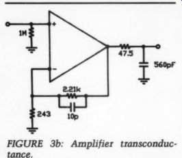
FIGURE 3b: Amplifier transconductance.
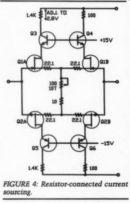
FIGURE 4: Resistor-connected current sourcing.
...similar (probably from the same die), also worked very well with a small heatsink. Granted, the above transistors are not the newest ones and may not be available in your area, but if they are, you should consider them. In the course of my later work I also found a number of other suitable transistors-I will come back to these later. As for the current in the second stage, after trying quite a few different values, I ended up selecting about 30mA, which is the same as the combined current of the second stage and the follower output in the original lineamp. (It also happens to be the current I used in the second stage of the 60W power amplifier, as you may recall.) This current is a good compromise between linearity, power dissipation and load-driving capability.
Enhanced Stability
Using this Class-A stage as the out put also simplifies the circuit in terms of stabilizing it. As you know, a follower output stage is always difficult to include in a feedback loop due to its phase shift. Getting rid of the follower reduces the phase shift and allows you to work with a significantly wider bandwidth. Also, the second stage has a very high output impedance, which is easy to roll off with a capacitor. 1 have stabilized the amplifier with an RC network at the output, the R serving as an isolation resistor. The advantage of this is that additional capacitive load will make the amplifier more stable, instead of unstable as the case usually is with a follower output.
Coming back now to the input stage, I have done two more modifications, partially to reduce the cost of the amplifier further, but also with more improvements in mind. The constant cur rent sources feeding the differential in puts are working okay and were originally designed to allow you to use FETs with a wide range of I_DSS without adjustment. However, if you accept a simple adjustment, then you can get rid of the constant current sources. This is due to the fact that the source of the N-channel FET is positive relative to the gate and the source of the P-channel is negative, so you can connect the two tails together through a resistor, one acting as the current source for the other. The principle is shown in Fig. 4.
The idea is not new. You might remember John Curl using this technique in the JC-2 amplifiers. Besides saving components, you can expect an improvement in common mode rejection;
since you have no constant current sources, no unwanted signal can get in to the input that way. The only draw back is that due to the I_DSS tolerances an adjustment is required to set up the current in the input stage. However, this is a very simple adjustment: you connect a voltmeter across the 1.4k collector resistor and adjust the voltage drop to approximately 2.8V.
In the I group I have called for BL input FETs. This is necessary for adjusting
the current to 2mA in each transistor using the method described above. Remember,
there is a voltage drop across the source resistors and since the 2SK240/28SJ75
FETs are working with a low gate-source voltage any way, you might run out
of voltage when adjusting the current. This “tail” resistor can be zero ohms;
the reason you see a small resistor in series with ... 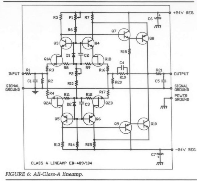
FIGURE 6: All-Class-A lineamp.
... the trimpot is because I like to limit the maximum current. I have built a number of these amplifiers using BL devices and have always been able to adjust the current to 2mA with 22.1 ohm source resistors. If you would like to experiment with 100 ohm source resistors for greater input overload capability and better linearity, you might not be able to use all BL devices, but just the ones with I_pss at the higher end of the range.
Alternatively, you can extend the range of usable devices by reducing the input current to 1mA per transistor. Naturally, you have to change the collector resistors to accommodate this. The only thing to remember is the current conversion between the input and second stage.
The second change I made concerns ...
+24V REG.
OUTPUT SIGNAL GROUND POWER GROUND
-24V REG.
... mainly the input swing capability, but offers additional benefits as well. If you use the amplifier as a unity gain follower, the input voltage and the out put voltage are the same. For a 10V RMS output, the input has to be able to swing 10V RMS. If you look at Fig. 5, you will see that the cascodes have a fixed bias of 15V, meaning that the input FETs are operating with a drain source voltage of approximately 14.5V.
Assuming that the input FETs need 1-2V D-S voltage for proper operation (this depends very much on the type of FET you are using), you can move the input up and down only about 12V peak before you saturate the input FETs.
You can avoid this by referencing the cascode bias to the source of the FETS, so the cascode bias moves up and down with the input voltage. This common mode feedback keeps the drain-source voltage of the input FETs at a constant level, independent of the voltage swing at the input. This way, you can extend the operation of the input stage close to 20V peak. The principle is illustrated in Fig. 5. A reference diode is connected between the bases of the cascode transistors and the intersection of the FET source resistors. I am using LM336Z-2.5V reference diodes, but others are also applicable. The reference diode is supplied with a current of approximately 1mA; however, this depends again on the type of reference diode used. With regulated supplies you can get away with a resistor to supply this current. Otherwise, you should use constant current sources. The advantage of using resistors is that it allows you to do a simple offset adjustment with the same resistor. The reference diode should be bypassed with a 0.1uF ceramic or film capacitor for high frequency stability. The current flowing through the diode also flows through the “tail” resistor, so this resistor has to be readjusted to keep the current in the input stage at the desired value.
Additional benefits of using this arrangement are reduced input capacitance and improved linearity at higher input levels. The reduction of input capacitance is very important when using the 2SK240/2SJ75 FETs. The original lineamp using NPD/AH transistors had an input capacitance of about 10pF.
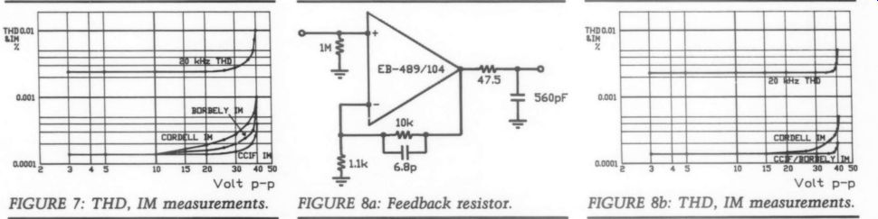
FIGURE 7: THD, IM measurements.
FIGURE 8b: THD, IM measurements.
Due to the significantly higher internal capacitances of the 2SK240/2SJ75, our input capacitance has now increased to approximately 40pF. This can cause stability problems, especially when the amplifier is used with higher-value feedback resistors. Using the cascode arrangement shown in Fig. 5, the input capacitance has been reduced to about 4pF, which makes life much easier when applying feedback around the amplifier.
Testing the Lineamp
The all-Class-A lineamp is shown in Fig. 6. Although I still keep calling it “lineamp,”' it is actually a general purpose, high quality, discrete Class-A operational amplifier. Let's now see how it fares with our linearity and other measurements.
I tested the amplifier extensively in the configuration shown in Fig. 3b.
This is a noninverting amplifier with a gain of 10x or 20dB. In order to evaluate the open-loop performance of the amplifier, I bypassed the 243 ohm resistor by using a bank of capacitors totaling 57,000uF. This short-circuits the minus input AC-wise, but preserves the DC feedback. The 2.21k resistor acts as a load on the output. Under these conditions, I measured the following open-loop performance:
Gain: 400x (52dB)
Freq. Res.: 90kHz (-3dB)
THD: 10V RMS/1kHz: 0.04%
/20kHz: 0.04%
/100kHz: 0.07%
As you can see the amplifier has very good open-loop linearity at high frequencies, which, coupled with the very wide open-loop bandwidth allows you to utilize feedback in an efficient way.
And efficient you must be, because you don't have too much of it: the feedback is equal to open-loop gain minus closed loop gain, which is 32dB. But then again, you don't need too much of it, because the linearity is very good any way.
Removing the 57,000uF bypass and measuring the amplifier in the + 10x configuration yields the following results:
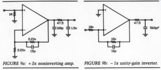
FIGURE 9b: - 1x unity-gain inverter.
Input cap.: 3.2pF
Input noise: 0.654V (20Hz-20kHz, RMS)
Output imp.: 75 ohm (at 20kHz)
Freq. Res.: 2.5MHz (-3dB)
Rise time: <200nsec (0-10 peak)
Slew rate: 100V/usec
Total harmonic distortion at 1kHz is not measurable on my equipment. The 20kHz THD and the three IM measurements are shown in Fig. 7. The 20kHz increase at very high levels is due to saturation effects in the second stage of the amplifier, and is almost purely third harmonic. This is also clear from the CCIF measurement, which, not being able to detect odd-order products, shows very low values of distortion.
The Cordell IM is the most sensitive measurement for this circuit, because of its sensitivity for odd-order products.
Knowing that the open-loop gain is very low and depends on the load on the second stage I was curious to see if an increase in open-loop gain and a corresponding increase in feedback would further linearize the closed-loop behavior of the circuit. Consequently, I changed the feedback resistor from 2.21k to 10k as shown in Fig. 8a. With the 10k feedback resistor (which is also the load on the output), the open-loop gain increases to approximately 64dB, which in turn increases the feedback to 44dB. The 20kHz THD and the three IM measurements are shown in Fig. 8b.
The Cordell IM is still the most sensitive to detect the onset of saturation--the other measurements can only detect the clipping itself. Whether you can hear the difference between the two circuits is up to you.
It should be clear from the above measurements that the amplifier can't drive very-low-impedance loads, such as 600 ohm. It is important to remember that this is not only a question of second-stage current, but also of the open-loop gain, which is very low with such a low-impedance load. Let's face it, when you need to drive very-low-impedance loads you must go back to a real power output, for example, a follower, which isolates the load from the second stage. However, the amplifier is capable of driving all practical audio loads larger than 2k ohm without problems. Most important, due to its extreme stability it can drive capacitive loads easily; an extra 1,000pF, corresponding to a cable of 10-15 meters, makes very little change in any of the above specifications. I think the combination of all-Class-A operation, extreme stability and very good linearity makes this topology a very interesting candidate for audio use.
Obviously, you should also be able to use a general purpose amplifier in other than + 10x configurations. I have tested the amp in both noninverting and inverting configurations and will show two of these here. Figure 9a shows the amp in a +2x (6dB) con figuration and Fig. 9b, in a -- 1x, or unity gain inverter, configuration. (Al though it is possible to stabilize the amp for + 1x or unity gain follower operation as well, I will not show it here since I have other, more suitable topologies for this.) The reason for presenting the amplifier in the +2x configuration is because many of you mentioned that the standard + 10x or 20dB lineamp has too much gain when used with CDs. Well, you might want to consider this configuration if you are only listening to CDs.
Since the feedback factor is the same in a +2x and a - 1x configuration, the specs are very similar for the unity gain inverter shown in Fig. 9b. Although I ...
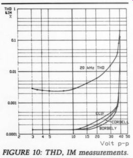
FIGURE 10: THD, IM measurements.
... haven't tried it, the low input capacitance, the very wide bandwidth and the very good linearity might suggest this configuration as a current-to-voltage converter in CD players. Any volunteers to try it? The RIAA-1 One of the other amplifiers I dissected and reworked was the RIAA-1 from the Borbely preamplifier (TAA 4/85, Fig. 11, p. 12). Originally, I selected this topology for its low noise and high speed; it has been optimized for low noise in the RIAA-1, RIAA-1 V.2 and the MC preamps. The basic topology of this circuit has also been used in my tape buffer.
Some time after the publication of the original preamp, I decided to try this topology for a high-speed lineamp.
The first attempt was simply a stripped version of the RIAA-1 board, which was sufficiently promising to prompt further investigation. Later, I redesigned the RIAA-1 as a lineamp and introduced it in 1987. Many readers have purchased the version called LINE388 and praised it for its speed, low noise and very clean sound. However, the purpose of this exercise is first to look at the RIAA-1 topology in general and then to see whether the improvements make it useful in any particular application.
I have measured the RIAA-1 as a linear amplifier i.e., through bypassing R25-C18. The 20kHz THD and the three IM measurements are shown in Fig. 10. Considering that this topology has been optimized for low noise and that linearity was only a secondary concern, the RIAA-1 fares reasonably well, but it also shows that its open-loop linearity could be improved. With a moderately high open-loop gain of 80dB and also a moderately high open-loop bandwidth of 12kHz, the closed-loop linearity should be better.
-----------------
TABLE 1
-------------------
Again, all three stages contribute to the nonlinearity. However, since the second stage is a normal common emitter stage with inherent linearity problems, it is the prime suspect where linearity is concerned. This stage must handle the whole output voltage swing; consequently, the transistors are working with a very wide range of collector-emitter voltages. A common emitter stage suffers from two major types of nonlinearity. One is called the Early effect: an increasing voltage across collector-emitter means an increasing reverse bias across the collector base junction, causing a decreasing base width, which results in an increasing emitter current. This shows up as an upward slope of the common emitter Ic/V characteristics on the curve tracer, limiting the output resistance of the transistor to a finite value3.
At high frequencies you have an additional nonlinearity caused by transistor junction capacitances. As I de scribed in Part I (TAA 2/89, Fig. 7, p. 11), the junction capacitances are a function of the voltage across the junction. These capacitances determine the open-loop gain of the stage at high frequencies, and if you modulate the junction capacitances with the audio signal, distortion results.
The most efficient way of improving the static nonlinearity caused by the Early effect and the dynamic nonlinearity caused by the junction capacitance modulation is to use a cascode configuration. The cascode connection is not new, having been invented back in the good old tube days (oops, sorry, tube fans!); it has been used for high frequency amplifiers ever since. Due to its inherently wide bandwidth and good linearity, it has also found its way into audio amplifiers.
I believe the first all-out attempt to take advantage of the cascode configuration in audio was published by Nelson Pass in Audio. I first used the cascode connection in the driver and out put stage of the Dynaco ST-400. Although the primary reason for using series-connected transistors was power sharing,' an equally important achievement was its linearity. (For the record: I designed only the driver/output stage of the ST-400; the rest of the active circuitry was designed by Jim Bongiorno.
If you are not familiar with the ST-400, you can see this output stage in Jim's Ampzilla from GAS, as shown in Audio June, 1988, Fig. 3, p. 53.)
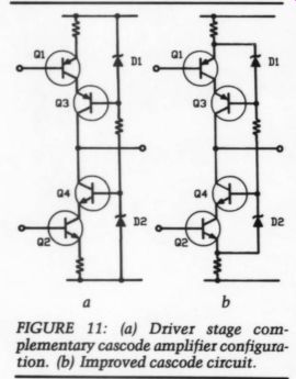
FIGURE 11: (a) Driver stage complementary cascode amplifier configuration.
(b) Improved cascode circuit.
An All-Cascode Approach
My second cascode circuit appeared in a power amplifier I published in Wireless World,” where I used it as a high-current, Class-A driver for two pairs of MOSFET output devices. Since then I have been using cascode circuits in many important stages in my amplifiers. However, | haven't attempted an all-cascode approach until now. I also see a trend toward using cascodes in high- end audio in general, but again, not in all stages as proposed by Nelson Pass. Also, cascode circuitry has never captured the attention of audiophiles as Class-A has, for example, although I believe it is one of the most important improvements in audio design.
Enough history-back to the second stage of the RIAA-1. Figure 11a shows the basic configuration for a complementary cascode amplifier as used in the driver stage in my WW power amplifier. Transistors Q1 and Q2 are operating in common emitter configuration, while Q3 and Q4 are working in common base mode. Requirements for Q1 and Q2 are high gain, good hg linearity and low saturation voltage at the operating current. If Q1 and Q2 don't have high enough hg, they load the input stage, reducing the effective open-loop gain. You can use an emitter follower in front of Q1 and Q2, as I did in the WW design. However, followers introduce additional phase shift which you must take care of when stabilizing the amplifier. I prefer to use single transistors with high hg and operate them at a relatively high cur rent to get a good I;/ Vy linearity.
Requirements for the common base transistors Q3 and Q4 are high Early voltage (which determines the output resistance), low saturation voltage and low collector-base capacitance. The bias for these transistors is generated with a string of diodes, a low-voltage zener diode or an active reference diode; it needs to be a couple of volts. You can also use low-leakage green LEDs with a forward voltage drop of approximately 1.6V. I prefer to use the LM336-2.5V reference diodes, which work in most applications. A decoupling of these diodes with a 0.1uF film or ceramic capacitor is sometimes necessary for high frequency stability.
Figure 11b shows an improved version of the cascode circuit, which is a further development of my WW driver and is included in the LINE388 circuit.
I have seen this circuit used in high-end designs and you can find a comprehensive description of it in JAES. This connection is bootstrapping the base of the common-base transistors to the emitter of Q1/Q2, further decreasing the loading effect of the junction capacitances and improving high frequency linearity.
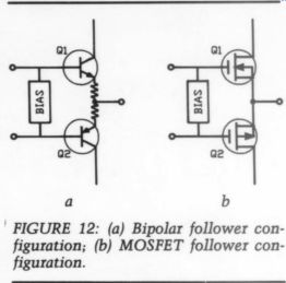
FIGURE 12: (a) Bipolar follower configuration; (b) MOSFET follower configuration.
Choosing Transistors
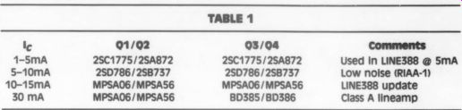
As for the type of transistors used in this stage, it all depends on the application and the current at which you want the second stage to run. If you only need up to, say, 5-mA, the 2SC1775/ 2SA872 pair can do a good job for all positions. (I used these in the LINE388.) For low noise applications and currents up to about 10 mA, the Rohm 2SD786/ 2SB737 pair is preferable. For general purpose applications with currents in the range of 10-60mA, the MPSA06/ MPSAS56 transistors work very well for position Q1/Q2. For high current, you will need a pair with higher power dissipation capability for Q3/Q4. I have found the BD385/BD386 to work very well in these positions. Table 1 shows some of the combinations for different applications.
Leaving the second stage for a moment, let's look at the output stage, which is also a major contributor to non linearity. Although there are many ways to design an output stage, I will concentrate here on the emitter/source follower because this is the most widely used one in preamp stages such as the RIAA and line-amps. The basic follower configurations for bipolar and MOSFET are shown in Fig. 12a and 12b, respectively. Note the emitter resistors in the bipolar stage: they are necessary for thermal stability. The corresponding transconductance characteristics (trans
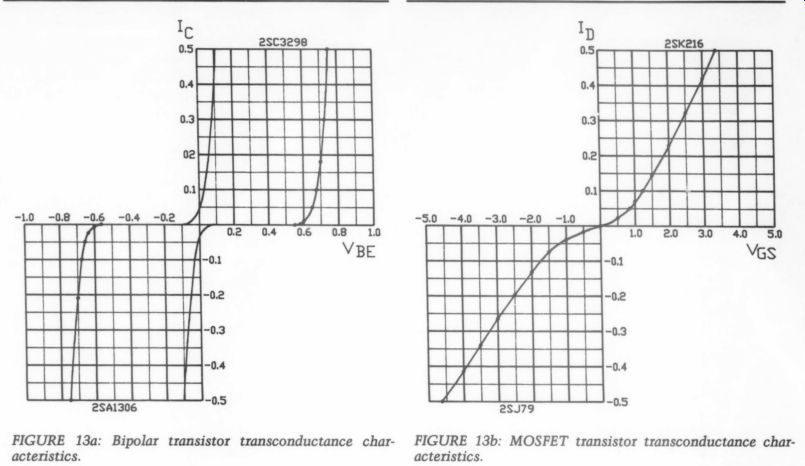
FIGURE 13a: Bipolar transistor transconductance characteristics.
FIGURE 13b: MOSFET transistor transconductance characteristics.
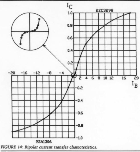
FIGURE 14: Bipolar current transfer characteristics.
fer characteristic, when the device is driven from a constant voltage source) are shown for typical bipolar and MOSFET transistors in Fig. 13a and 13b. 1 have chosen a Toshiba complementary pair for the bipolars, which are rated at 160V breakdown, and a
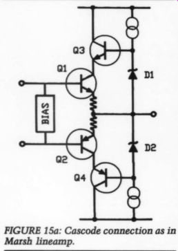
FIGURE 15a: Cascode connection as in Marsh lineamp.
maximum collector current of 1.5A.
They come in a TO-220 look-alike package in which the collector tab is also covered with molded plastic, thus not requiring any insulation when mounted on a heatsink. The MOS-FETs are the well-known Hitachi 2SK216/ 2SJ79 devices, rated at 200V breakdown but with a maximum drain current of 0.5A. I could have chosen a more “modern” MOSFET, such as a pair of IRF611/IRF9611 HEX-FETS, but because of their high gate threshold voltage I only use them in special applications.
This shouldn't prevent you from experimenting with these or similar devices, should they suit your application.
The transconductance characteristics of the two bipolar devices are very similar but obviously not 100% matched.
To get rid of the dead zone of +0.6V, they must be forward-biased, as indicated by the two curves near origo. The MOSFETs differ significantly from the bipolars in transconductance (dI,/ dV); they are much lower in absolute value. You will also notice that the N-channel and the P-channel are different, the P-channel having a lower transconductance.
We have said that the transfer characteristics in Fig. 13 are valid when the devices are driven from a low-impedance, constant voltage source. However, in most cases the follower is driven from the second stage of the amplifier, which, as we have just pointed out, should have a very high output impedance for good linearity. This does not make much difference to the MOSFETs, because they are, like tubes, voltage-driven devices with very high input impedance. But it makes a significant difference to the bipolars, because they are voltage- and current-driven devices and behave differently when driven from a voltage source (low impedance) and from a cur rent source (high impedance).
The easiest way to illustrate this is to look at the current transfer characteristics for the bipolars (Fig. 14), which show the relationship between I and Iz. The linearity of the current transfer is quite good up to 0.4-0.5A. However, the extended curve to 1A collector cur rent shows that you will get significant nonlinearity when using them above this value. Of course, you will only need such currents if you use this transistor as a driver in a power amplifier; in a lineamp, you will work with (may be) up to 100mA. You will also notice that the NPN and PNP transistors have a different steepness. This is strictly a trick from my side, because I tried to illustrate that the two can have different hgs. The transfer characteristics are also very nonlinear at very low collector currents, as I tried to illustrate with the magnified area around origo.
Naturally, because you can't drive the ...
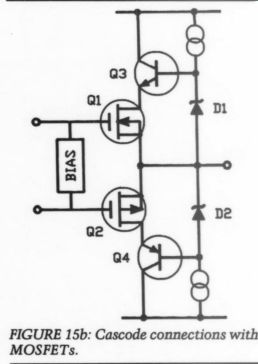
FIGURE 15b: Cascode connections with MOSFETs.
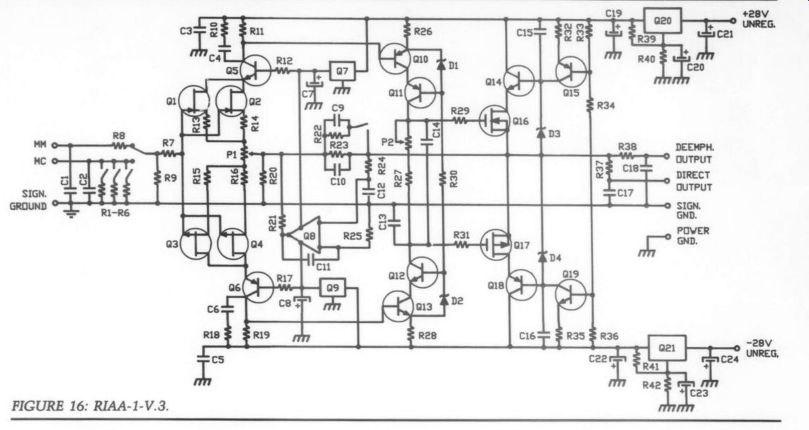
FIGURE 16: RIAA-1-V.3.
... two halves of the follower from two in dependent current sources in an easy way, you will still need a normal bias circuit to avoid crossover distortion.
'Should I drive the bipolars from a constant voltage source or a constant current source?' you might ask. Well, the answer is easy: you don't have much choice. They are driven from high-impedance, current sources in most cases. In case you are interested, there is an optimum source impedance for minimum distortion, but a treatment of this is outside the scope of this article. As far as I am concerned, I make the second stage as linear as possible, and then see what I can do about the linearity of the output stage.
At high frequencies, the device capacitances make the linearity problem worse. In the case of the bipolars, you have to deal with the charge storage in the base! (strictly speaking, this is only a problem with low f; devices!), and generally, with all the junction and parasitic capacitances. In case of the MOSFETs, the input capacitance plays an important role, in that the second stage has to be able to drive this with the required slew rate.
Again, cascode to the rescue. Figure 15 indicates the two most likely combinations of cascode connection, al though you might also consider others.
You will recognize Fig. 15a as being the same as the output stage in the Marsh
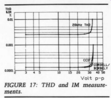
FIGURE 17: THD and IM measurements.
lineamp. I prefer the circuit with the MOSFETs in Fig. 15b because of the high-input impedance and the negative tempco of the MOSFETs. I use the LM336Z-2.5 or the LM336Z-5.0 reference diodes instead of the zener diodes, which normally require more current.
For the current sources you can use the FETs shown in TAA 1/89 (Fig. 3a, p. 30), or simple transistor current sources.
I have chosen to use these in the amplifier I have put together using the above described second and output stages.
Figure 16 shows the new version of RIAA-1 (RIAA-1-V.3), which is an all cascode, low-noise amplifier. You will notice that this is actually an update of RIAA-1-V.2, not the first RIAA-1. I have not changed the input stage topologically, partially because I haven't seen any need for it, but also because it is difficult to improve in any way without sacrificing its noise performance. I did change to GR devices because of better availability; this requires a change of source resistors. You can use the dual 2SK146GR/2SJ73GR or the single 2SK147GR/2SJ72GRs. If you have ac cess to the BLs, then you can use these as in the original RIAA-1-V.2.
I have also yielded to many readers' suggestions and replaced the 15V zeners, feeding the cascodes and the servo amp with 78L15 and 79L15 regulators. Please let me know whether it really improves the sound. The second stage is using the Rohm transistors operating at 10mA. The cascode transistors are referenced with LM3362Z 2.5V diodes, which are bootstrapped to the emitters of Q10 and Q13. The out put stage is the same as that shown in Fig. 15b; however, the constant current sources have been realized with MPSAQ06/MPSA56 transistors. I am using the 2SC2592/2SA1112 TO-220 complementary pair for the cascodes.
They are referenced with LM336Z-5.0 diodes, which are supplied with a constant current from the MPSAs: Q15/ Q19. The amplifier has two outputs: a de-emphasized one with R38 = 7500 and C18 = 0.1uF, and a direct one with R37 = 47.5 ohm and C17 = 1.5nF, which also serves as part of the overall frequency compensation network. As shown, the feedback network allows you to set the gain for 26 or 32dB. (R22= R23 = 133 ohm, R20 = 6.819).
The RIAA-1-V.3 produced the following open-loop measurements:
Gain: 72dB
Freq. Resp.: 15kHz THD: 10V RMS/1kHz: 0.02%/20kHz: 0.045%
The excellent open-loop results come from the cascoded second stage and the cascoded output stage. As you have seen earlier (and will see in the description of the LINE388), the bulk of the
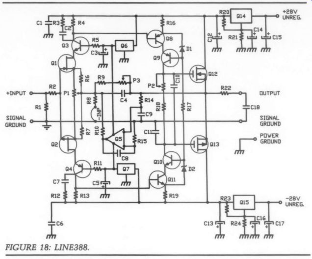
FIGURE 18: LINE388.
high-level THD is produced by the out put stage and one way to get rid of it and the three IM measurements for a gain setting of 26dB are shown in Fig. is to use a cascode. The 20kHz THD 17. Closed-loop frequency response is
--------------
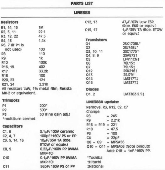
PARTS LIST--LINE388
------------------------
... down 3dB at 1MHz, rise time is 300ns for a 0-10V step and slew rate is around 40V/ps. Noise performance is practically the same as in the original RIAA 1-V.2. Let our kind Editor know if you are interested in the RIAA-1-V.3 and I will publish the layout and stuffing guide in an upcoming issue of TAA.
Figure 18 shows the schematic of LINE388, which I have been using for a couple of years. As you see, it is a simplified version of the RIAA-1 circuit, notably with a single pair of input transistors and a normal MOSFET follower at the output. Due to the follower, the open-loop THD is higher than that of the RIAA-1. But because of other changes in the circuit, the open-loop gain and consequently also the feed back factor is also higher, which reduces the intermodulation products to a very low level in the middle of the audio range.
Let's see the open-loop measurements:
Gain: 97dB
Freq. Resp.: 2.7kHz
THD: 10V RMS/1kHz: 0.4%
/20kHz: 0.45%
The closed-loop 20kHz THD and the three IM measurements are shown in Fig. 19. The slowly increasing 20kHz THD above approximately 12V peak to-peak is caused by the output stage, as you have seen before. The CCIF is detecting this increase but is barely out of noise. The other two IM measurements show no nonlinearity. Naturally, 1kHz THD is also below the measurement floor of my instrumentation. Rise time for the LINE388 is 0.2us for a 0-10V step. The closed-loop frequency response is down 3dB at 2MHz.
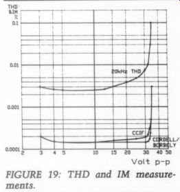
FIGURE 19: THD and IM measurements.
------------------
LINEAMP 388
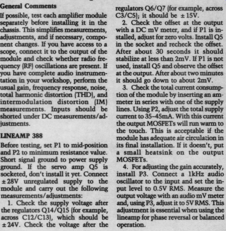
Setup Procedure
nent changes. If you have access to a scope, connect it to the output of the module and check whether radio fre the regulators Q14/Q15 (for example, across C12/C13), which should be +24V. Check the voltage after the regulators Q6/Q7 (for example, across C3/C5); it should be +15V.
2. Check the offset at the output with a DC mV meter, and if P1 is in stalled, adjust for zero volts. Install Q5 in the socket and recheck the offset.
After about 30 seconds it should stabilize at less than 2mV. If P1 is not used, install Q5 and observe the offset at the output. After about two minutes it should go down to about 2mV.
3. Check the total current consumption of the module by inserting an am meter in series with one of the supply lines. Using P2, adjust the total supply current to 35-45mA. With this current the output MOSFETs will run warm to the touch. This is acceptable if the module has adequate air circulation in its final installation. If it doesn't, put a small heatsink on the output MOSFETs.
4. For adjusting the gain accurately, install P3. Connect a 1kHz audio oscillator to the input and set the in put level to 0.5V RMS. Measure the output voltage with an audio mV meter and, using P3, adjust it to 5V RMS. This adjustment is essential when using the
--------------------
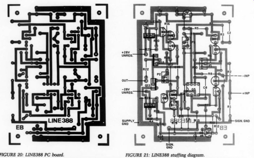
FIGURE 20: LINE388 PC board. FIGURE 21: LINE388 stuffing diagram.
The above measurements were taken on the updated version of the LINE388.
The major modification is the replacement of the second stage transistors with MPSAs and the increase of the current through them to approximately 10mA, which improved linearity a bit.
A rework of the frequency compensation network, which includes the removal of the input compensation (R3/ C2 and R12/C7) and the addition of C18, yields a slight increase in speed and closed-loop bandwidth. Using this compensation, the amplifier is capable The author resides overseas so if you wish to contact him and receive a reply, send your letter to Audio Amateur and enclose a large self-addressed envelope, and include two international postal coupons, available at your post office.
Readers interested in RIAA-1-V.3 should let our editor know by responding with FAST REPLY of driving larger capacitive loads than before. The layout is the same, so you can implement both versions using the same PC board.
Let's now look at the schematic for a moment. The input FETs are BL types. For optimum performance they should be matched to within 10% of Ipss- They are operating at about 2mA (accomplished by source resistors R6/ R7 = 1000). If you prefer to operate the LINE388 without servo, then you must replace R6/R7 with a trimpot: P1 = 2009. The cascode transistors Q3/Q4 are referenced from Q6/Q7 voltage regulators (78L15/79L15), which also supply the servo amplifier Q5. The second stage was using the 2SA872/2SC1775 transistors at 5SmA in the first version; in the updated version they have been replaced by MPSA56/MPSAQ6 transistors, operating at approximately 10mA.
The output stage uses the well-known Hitachi MOSFETs: 2SK216/28)79.
The regulators are LM317/LM337s. The feedback network consists of R9-P3 and R8, which is chosen to give the stand and gain of 20dB. One end of R8 is not connected permanently to ground and is available as a ( - ) input. For normal operation, this has to be grounded. For special applications, such as reversed phase output or balanced output, this is used as an inverting input. PC board layout and stuffing guide are shown in Figs. 20 and 21, respectively. For initial testing/ adjustment of the LINE388, see "Setup Procedure.” Here you might ask why I didn't apply my own recommendation to the output stage of the LINE388 and in stead used a cascoded one, as in the RIAA-1-V.3. It is possible to do it, and rest assured I tried it and it works. You can in fact make the 20kHz THD and the three IM curves absolutely flat at the residual level up to clipping. Due to the limited real estate on the PC-board I haven't been able to do it, and I firmly believe that the LINE388 is an excellent lineamp as is. However, this should not prevent you from trying it. After all, that's what this whole article series is all about. I want to challenge you to try to evaluate the different improvements and report back to the audio amateur community through TAA. That's the way we can improve the quality of our hobby. Good listening!
ACKNOWLEDGMENT
Dr. Kalman Molnar's help has been, through discussions and by reading the manuscript, invaluable. I greatly appreciate his contributions.
REFERENCES
1. Cordell, R. R., 'Another View of TIM,” Audio, February/March 1980.
2. Curl, John, “JC-2 Preamplifier,” TAA 3/77, p. 48.
3. Lowe, Jr., Brian, Letter to the Editor, TAA 4/86, p. 48.
6. Sweeney, D. and S. Mantz, 'An Informal History of Solid State Amps,” Audio, June 1988.
7. Borbely, Emo, “High Power High Quality Amplifier Using MOSFETS,” Wireless World, March 1983.
8. Hawksford, Malcom, “Reduction of Transistor Slope Impedance-Dependent Distortion in Large-Signal Amplifiers,” Journal of the Audio Engineering Society, Vol. 36, No. 4, April 1988.
9. Oliver, B. M., “Distortion in Complementary-Pair Class-B Amplifiers,” Hewlett Audio, March 1978.
23, 1962.
4. Pass, Nelson, “Cascode Amp Design,” Packard Journal, Vol. 22, No. 6, February 1971.
10. Howe, Thomas, 'Stretching Marsh's Preamp,” TAA 1/89, p. 29. 5. Stone, J. , US Patent #3,018,433, January
++++++++++++++++
Also see: