A good-quality FM communications receiver must be capable of reproducing the transmitted information as intelligible audio, with little noise, at the speaker. For this reason, amplitude modulation was mainly given up as a faithful means of two way radio communications. AM suffers from all kinds of noise, both natural and man-made. The transmitted wave is subject to so many kinds of interference that, before it is received, it quite frequently has picked up enough extraneous noise signal to make reproduction unintelligible. Noise pulses produce variations in the amplitude radio signals and are therefore very troublesome in AM operation. The hum of power lines, spark of the ignition system in an automobile, running of a motor, and even atmospheric disturbance are but a few of the sources of interference to these signals. However, the noises that bother AM do not cause interference in FM reception because they affect only the amplitude of the signal, not the frequency. In an FM transmitter, as previously explained, the audio modulation causes excursions of the frequency-not amplitude, as in AM. Therefore, any amplitude variations of the FM wave (and there are many, due to the same noise sources as for AM interference) are not reproduced in the receiver. Instead they are removed from the signal by the limiter stages. As a result, only frequency variations are converted into audio.
Even within the FM class, some types of equipment perform better than others. For example, a single-conversion FM super heterodyne has poorer combined overall image-frequency and adjacent-channel rejection than one having dual conversion.
Fig. 3-1. A double superheterodyne receiver.
To achieve good adjacent-channel rejection with a single conversion receiver, a low IF value is necessary. This, however, does not provide good image rejection. On the other hand, if good image rejection is needed, the high IF required impairs the rejection of adjacent-channel signals. By combining both a high and low IF in one receiver, both good image and adjacent-channel rejection are obtained; such a receiver (Fig. 3-1) is known as a double superheterodyne. The action of producing two IF's is basically that of generating first one IF, amplifying it, and then using it to generate a second IF. This is accomplished by mixing the received RF signal with a high frequency oscillator signal, as shown in the block diagram of Fig. 3-2. This combination of RF and oscillator signals produces the high-frequency IF necessary for good image-frequency rejection, which is obtained in the tuned selective circuits of the IF amplifier. After one or two stages of amplification, the high-frequency IF signal is injected into a second mixer stage and combined with a low-frequency oscillator signal. This mixing action produces the low-frequency IF necessary for good adjacent-channel rejection. Actually, most of the adjacent-channel interference is removed from the low IF by the selective filter which comprises several LC resonant circuits very sharply tuned to the exact bandwidth of the low IF. This means that practically no adjacent-channel or even image-frequency interference gets into the low IF's; therefore, the signal at this point is fairly clean. However, there is still the problem of amplitude variations (noise) in the IF signal; if these were to get into the discriminator, they would be partially reproduced and heard as noise in the speaker. To get rid of this noise, the FM receiver uses a limiter which works just like the one described in the audio section of the transmitter; that is, an incoming grid signal will increase the plate current up to a certain point. Beyond that point a larger (higher amplitude) grid signal will cause no further increase in plate current. Therefore, the noise pulses (because they produce the excessive amplitude excursions) are not passed by the limiter.
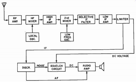
Fig. 3-2. Block diagram of a typical FM communications receiver.
You can see that the combination of the high and low IF's and the limiter literally wipes away all interference and noise from the transmitted signal. This "clean" signal is then changed back into audio by the discriminator, boosted in strength by an audio amplifier, and then fed to the speaker where it is converted into sound energy. While no interference may be heard in the speaker when a signal is present, there certainly will be noise while no signal is being received. A certain amount of noise is produced in each stage by electrons as they flow through tubes and other components. Tubes in particular generate considerable noise due to thermal effects, mechanical vibrations, etc. The noise produced in each stage is amplified and passed along to the next stage, where it is treated like a weak radio signal. Every tube produces some noise; in a 15- or 20-tube receiver, considerable noise builds up. As an example, the noise produced in the first RF amplifier is amplified by this stage and then injected into the following. Here it is further amplified and so on right down the line, picking up and amplifying the additional noise contributed by succeeding stages and finally being heard from the speaker. By now it is so un bearably loud that the radio listener has to turn the volume down to keep from becoming fatigued. To prevent this, a built in squelch circuit blocks the audio stage until a signal is received. Notice in Fig. 3-2 that the squelch circuit is between the discriminator and audio amplifier. Because there is no limiter action with no signal present, the squelch circuit effectively cuts off the audio amplifier, and the speaker is silenced.
When a signal causes the limiter to go into heavy conduction, this squelch action is killed and the audio amplifier once again performs its normal function.
RF AMPLIFIERS
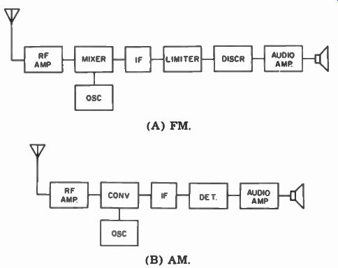
Fig. 3-3. Block diagrams of FM and AM receivers. (A) FM. (B) AM.
The receiver of a typical two-way radio is shown in Fig. 3-1. Each coil can has a tunable slug inside it to permit periodic adjustment. Fig. 3-3A shows the block diagram of a basic FM receiver. In spite of the apparent similarity to the standard AM receiver in Fig. 3-3B, the FM receiver is actually quite different, as you will see in this section. The requirements of FM are the same as for AM, only more stringent. Perhaps the most important is high sensitivity, which is determined by the minimum RF signal-voltage input required to produce a specified output at the speaker. The most sensitive receiver is one that will faithfully reproduce the greatest output with the smallest input signal.
The next major requirement of a receiver is its ability to select a desired station and to reject all others. Unwanted adjacent-channel signals are rejected by the bandpass characteristics of the IF amplifiers, while most of the incoming image frequencies are lost in the RF amplifiers and mixer. The combination of sensitivity and selectivity makes for a very efficient receiver.
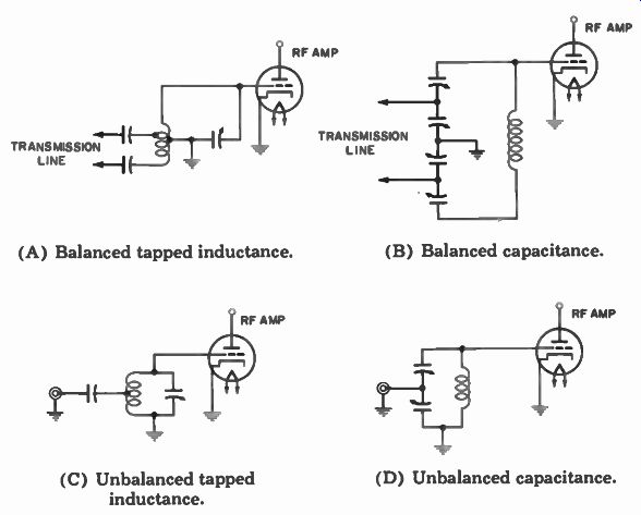
Fig. 3-4. RF-amplifier input circuits.
(A) Balanced tapped inductance.
(B) Balanced capacitance.
(C) Unbalanced tapped inductance.
(D) Unbalanced capacitance.
The signal is brought from the antenna to the RF amplifier by either a two-wire or coaxial transmission line. In an open insulator, two-wire line, the two signal voltages are equal in strength but opposite in polarity; therefore, a balanced input (Figs. 3-4A and B) is required at the RF amplifier input. however, since a coaxial line has its outside conductor at ground potential, an unbalanced circuit (Figs. 3-4C and D) is required.
With its inside conductor shielded, the coaxial line does not act like an antenna and pick up stray noise, as the two-wire line does. Since the noise voltages on both sides of the two-wire line are in phase with each other (each line being 90 degrees out of phase with ground), and since these noise voltages are 180 deg. out of phase with ground, the balanced input circuits will cancel them out. (The balanced input recognizes only signals out of phase with each other and 90' out of phase with ground.) The input circuit of an RF amplifier, whether balanced or unbalanced, usually consists of an input LC network. The part of the circuit "facing" the antenna is built to match the impedance (usually 50 ohms) of the antenna and transmission line, and the part "facing" the tube matches the high impedance of the grid-to-cathode input circuit to the antenna. The tuned circuit allows peaking of the resonant circuit to the incoming signal in order to effect maximum transfer of signal power.
The actual amplifier circuit must be capable of greatly improving the signal-to-noise ratio, suppressing the image frequencies, and preventing the local-oscillator signal from traveling back into the antenna and being radiated. These circuit requirements constitute a wide variety of design for RF amplifiers. Naturally the better-designed circuits found in many of the more expensive receivers will give a more satisfactory over all performance than one of poorer design.
RF Amplifier Problems
The RF amplifier, being the first stage of the receiver, naturally affects all following stages. In today's modern narrow band communications receivers, the RF section must be critical in accepting the required signal and still reject all others.
This is hard to do, since the resonant antenna circuit must be broad enough to be tuned over a complete band. Because so many stations operate on the same or on adjacent frequencies, the problems of intermodulation and desensitization are more acute than they were in the earlier days of FM. These two conditions occur during reception of undesired RF signals in the RF amplifier circuit. Desensitization is the condition where by an off-channel signal causes the amplifier grid to draw current on the positive peaks. This increases the grid bias and thus reduces the stage gain. Desensitization means the receiver has become "de-sensitive" and requires a much stronger signal to operate. This can happen if a strong adjacent-channel signal gets into the RF circuit and is amplified. The signal will not pass all the way through the IF's because of their bandpass response; therefore the operator will probably be unaware that another station is interfering. However, if an "on-channel" signal is received, it now must overcome the interfering signal or the set will be effectively dead.
Intermodulation is also caused by undesired signals entering the RF stage, but does not kill the receiver. Rather, it is reproduced and heard as audio in the speaker. Providing it is strong enough, an "on-channel" signal will usually overcome this condition, and then only the desired information will be heard. Unlike desensitization, intermodulation occurs only when two signals of the proper frequency are present at the antenna at the same time. As an example, if a 52- mhz receiver has two signals-one at 52.12 and the other at 52.24 me-entering its antenna circuit, they will produce a resultant at 52 mhz.
Since the second harmonic of 52.12 mhz created in the mixer stage is 104.24 mhz, the difference between it and 52.24 mhz is 52 mhz-the center frequency of the RF circuits. Any modulation on either original signal will be recognized by and heard in the speaker.
Desensitization and intermodulation are strictly problems of selectivity; therefore, good RF amplifier design is important.
In normal use the amplifier seldom develops trouble. When a component does need replacing, however, the exact replacement should be used if possible, or the one closest to it. What a different value of component will do to help or hinder inter modulation and/or desensitization in a receiver is impossible to accurately predict. Just keep in mind that the original component was put there for a specific purpose, and you should not try to work around RF amplifier problems by trying to re build the circuits. They have been designed at the factory for optimum performance, and seldom if ever need reworking.
RECEIVER OSCILLATORS
Most communications receivers are double superheterodynes, which require two oscillators, each operating at a different frequency. The first, or high-frequency, oscillator output is mixed with the incoming RF signal to produce the high-IF frequency. This IF is then amplified and mixed with a signal from the second, or low-frequency, oscillator to produce the low-IF frequency. Since the local oscillator controls the front end of the receiver, any change here will be noticed in the following stages as it is amplified. The frequency stability of the first oscillator is much more stringent than that of the second (low-frequency oscillator). The local oscillator must be able to maintain the IF at the center of the bandpass for a given incoming signal frequency. If it should drift even slightly, the IF center frequency would shift to one side of the bandpass response and a poor signal would be reproduced.
Frequency Drift
Other than a bad crystal in an oscillator circuit, perhaps the most common cause of frequency drift is mechanical. Over a period of time, vibration changes the adjustment settings of inductors and capacitors, altering the circuit constants which control the oscillator frequency. Generally, this problem is overcome by securely mounting all components and by shock mounting the receiver to protect it from vibrations. Frequency drift also arises from voltage variations on the tube electrodes-a fluctuating B+ on the plate or screen, or an erratic cathode voltage. Any of these conditions can seriously affect the oscillator output; however, these are generally no problem with a good-quality power supply. Most B+ supplies have good voltage regulation, so electrical frequency drift is seldom en countered. Power supplies do go bad at times, however, and the trouble might show up first as frequency stability at the high-frequency end of the receiver.
Still another cause of frequency instability in an oscillator is thermal drift. Temperature variations cause coils and capacitors in the circuit to expand and contract, thus changing their circuit constants. This problem may be greatly lessened by using quality components having low-temperature coefficients. Air-dielectric trimmer capacitors depend on air for insulation. Since dry and moist air have different dielectric constants, the trimmer capacitance will undergo variations as the humidity fluctuates. This is easily amended by inserting the trimmer into a hermetically sealed chamber (leaving provision for adjustment, of course). Another method is to use a heating device near the trimmer to keep the air dry. In some circuits the trimmer can be mounted on top of the chassis, near the crystal oven (which becomes quite warm); or a small filament lamp bulb can be placed next to the trimmer.
High-Frequency Oscillator
In a high-frequency oscillator, the crystal doesn't oscillate at the desired frequency. Instead the oscillator operates on a crystal harmonic, and the desired working frequency is obtained by means of a multiplier stage similar to those employed in the transmitter. Fig. 3-5 illustrates the pentode crystal oscillator used in many communications receivers. This stage works like the one in the transmitter oscillator except it develops much less power. If excessive, power might leak through the RF amplifier stage and into the antenna, where it would be radiated and cause interference with other stations. The power requirement of the receiver oscillator is small because it only mixes with the incoming RF to produce the IF. In the transmitter, however, the oscillator must develop more power because it drives frequency multiplier-amplifiers.
In the VHF range of frequencies where most two-way radios operate, the local oscillator must operate at a very high frequency. An overtone or a harmonic crystal oscillator is there fore necessary. The harmonic oscillator is the lesser used be cause of the very high harmonic content in its output circuit.
If these harmonics are allowed into the mixer, serious difficulty from spurious responses may arise. Therefore, a special crystal is used which is made to oscillate on other frequencies very close to odd harmonics of their fundamental. The main ad vantage of this crystal oscillator is its relative freedom from harmonics below its oscillating frequency. To realize this feature, special circuitry must be employed that has some means of feeding back part of the output signal into the input circuit.
This feedback is not used for oscillating purposes, but rather to hold the rate of oscillations steady at the desired overtone.
The necessary energy is generally developed in the output resonant circuit and fed back either inductively or capacitively.
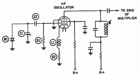
Fig. 3-5. Receiver high-frequency oscillator.
Notice in Fig. 3-5 that the combination of M1 and C1 forms the input parallel-resonant circuit. Oscillations will occur between the grid and cathode through cathode RF choke Li and resistor R2, ground, the input resonant circuit, and C2. The resultant flow of RF plate current is taken off through C3 and injected into the multiplier stage. Feedback is obtained in the grid circuit through L1, R2, and grid resistor R1 (which develops the required operating grid bias). This type of feedback should be small enough not to cause oscillations, but merely serve as a synchronizing signal for the overtone.
Like the transmitter oscillator, this type of receiver oscillator suffers from crystal frequency drift. This is the reason the high frequency crystals are enclosed in a thermostatically controlled oven. If normal temperature variations were allowed to affect the expansions and contractions of the crystal, the subsequent frequency drift would distort the received signal. In actual use the crystal oscillator requires only occasional adjustment as normal aging of the crystal and components gradually lowers the frequency (this normally will not happen for several years). The crystal should be replaced when the oscillator frequency becomes so low that the frequency-adjusting capacitor is no longer able to compensate. However most communications receivers are so well built that it is not uncommon for them to stay in service 10 or 15 years. Since the oscillator is the heart of the radio, it should be kept in top working efficiency by replacing the crystal if at all needed.
THE MIXER
The mixer stage in an FM receiver beats the applied RF amplifier signal against the injected RF oscillator signal in order to produce the intermediate frequency (IF). This mixing action in the electron stream of the mixer tube produces side bands at the sum and difference frequencies of the two applied signals. Generally the difference signal (lower sideband) is used as the IF, and since the local-oscillator signal is stronger than the RF amplifier signal, development of spurious side bands is kept to a minimum. However, if the oscillator signal happens to contain harmonics, they will also beat against the incoming RF signal and produce sidebands. To prevent these unwanted sidebands from feeding into the following stage, the output circuit of the mixer is designed to discriminate against all but the desired sideband. Generally this discrimination is accomplished by two or three very critically tuned (high-Q) resonant circuits following the mixer.
The low percentage of modulation required for frequency conversion can be produced in one of several ways; however, the most common method in communications receivers is de pendent on the transfer characteristic of the mixing device (the relationship of the input- to output-signal characteristic of the device). With a purely resistive device, any signal at its input may be lowered in amplitude at its output. Otherwise, the two signals will look exactly alike. In Fig. 3-6A the diagonal line represents the transfer characteristic of pure resistance plotted against the input voltage. Notice that the output is practically identical to the input. However, in a device such as a vacuum tube, the output is dependent on the familiar I„-Eg (plate current-grid-voltage) curve shown in Fig. 3-6B. The vacuum tube is a nonlinear device, and as you can see in Fig. 3-6B, only part of the grid signal is faithfully reproduced.
Any nonlinear device like a vacuum tube or a solid-state diode can be used as a mixer. In the vacuum tube, the RF signal is usually applied to the control or screen grid, whereas the oscillator signal is usually applied to the cathode or control grid. Both signals modulate the plate current. The output of the diode mixer is likewise modulated. When a diode is used as a mixer, whether vacuum tube or solid-state, the incoming RF signal is applied to the input circuit and the oscillator signal is coupled to the output of the mixer. Modulation then takes place because the incoming RF signal is impressed on the oscillator signal and causes the latter to vary in accordance. This mixing then causes sidebands, just as in the vacuum tube mixer.
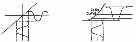
Fig. 3-6. Transfer characteristics. (A) Linear. B) Nonlinear.
Since a mixer is nothing more than a low-level modulator, it can produce many different IF frequencies according to the incoming RF signal and its sidebands, and the sidebands of the oscillator signal. If all frequencies but the desired RF are attenuated before arriving at the mixer, and if the oscillator is operating with low harmonic content, the mixer output will be very low in spurious responses. The most bothersome spurious response is the image frequency, which combines with the oscillator signal to produce a spurious sideband. As an example, if the oscillator is operated 1 megacycle higher than the RF signal, the image will appear 2 megacycles above the RF signal. If a strong carrier happened to appear at this image frequency (and it does quite often in two-way radio) it would interfere with reception of the desired station signal. A station does not necessarily have to be operating on the receiver image to create trouble. If the receiver is near a high-powered transmitter, any number of spurious responses are possible.
As previously stated, the mixer and RF amplifier circuits must be well designed, to keep the oscillator signal from leaking back into the antenna and being radiated. If this were to happen, it could cause interference in nearby receivers. In poorly designed mixers the weak oscillator signal is loosely coupled through the stray capacitance of the wiring. Even in well-designed circuits, however, stray capacitance is a problem. Another way the oscillator signal can get back to the antenna is via the capacitance of the mixer tube. If the in coming RF signal is injected at the control grid and the oscillator signal is impressed on the cathode, the capacitance between the two electrodes will effectively couple the oscillator signal back into the RF input circuit. Still another way the signal can get back into the input circuit is through the electron stream of the tube itself.
Typical Circuits
Diode mixers are used at the extreme upper end of the VHF range, where ordinary tubes are unsatisfactory. The diodes (whether vacuum-tube or solid-state) must have extremely small internal dimensions, and their anode and cathode must be close together. Since diode mixers function very efficiently with not only the oscillator fundamental but also the harmonics, oscillators operating at lower frequencies can be used.
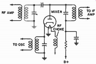
Fig. 3-7. Diode mixer.
Fig. 3-7 shows a typical diode mixer circuit. The parallel resonant circuit of the cathode is resonant at the oscillator signal voltage, and the capacitor is also used at the cathode RF bypass. The capacitance between the heater and cathode in most vacuum tubes is sufficient to kill the oscillator injection circuit if not isolated. This is one reason for using an RF choke in the heater circuit of the diode. Another reason is to keep RF from being coupled to other stages through the filament circuit.
Fig. 3-8 shows two triode mixer circuits commonly used in FM receivers. In Fig. 3-8A the oscillator as well as the incoming signal is injected at the control grid; in Fig. 3-8B, however, the incoming signal is coupled to the grid, but the oscillator signal is injected into the cathode circuit. As far as performance is concerned, there is little difference between the two circuits. With cathode injection, the grid loading effect is slightly higher than with grid injection; however, cathode injection gives better oscillator stability, since a low-impedance load is presented to the oscillator.
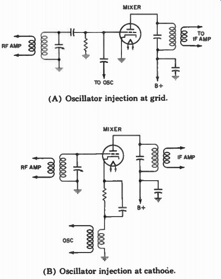
Fig. 3-8. Triode mixers. (A) Oscillator injection at grid. (B) Oscillator
injection at cathode.
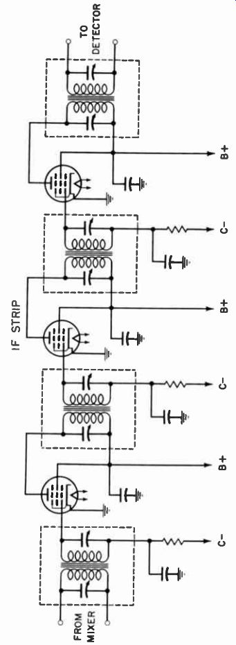
Fig. 3-9. A typical 3-stage IF-amplifier circuit.
THE IF AMPLIFIER
Considerable IF selectivity is required in communications receivers in order to prevent adjacent-channel interference.
However, the IF gain must also be increased when higher IF selectivity is desired. Because of difficulties arising from in stability and feedback in an IF system, there is a limit to the amplification-and therefore, the selectivity-obtainable. Be sides this, a high-frequency IF is needed in order to provide for good image rejection, but the high IF further lowers the selectivity obtainable. Therefore, the problem is met by using two IF frequencies to help reduce instability. The high IF provides the necessary image rejection, and the low IF the necessary selectivity.
In the conventional FM IF circuit shown in Fig. 3-9, the operation of the LC resonant interstage coupling transformer determines the gain and selectivity of the stage. In general, these transformers must be made adjustable so that the set performance can be controlled. The transformation coupling is determined in the design stage, and the transformer is built to these specifications. Since the efficiency of the resonant circuit must be kept up to par, however, either the capacitor or inductor is made adjustable.
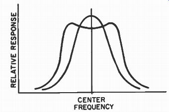
Fig. 3-10. IF response curve.
To gain the full advantages of FM reception, the IF system must have a selectable response that does not introduce objectionable distortion into the sideband system. At the same time, it must have sufficient adjacent-channel rejection. If the selectivity curve shown in Fig. 3-10 is not symmetrical about the center frequency, considerable distortion will appear in the receiver output because some sidebands are amplified more than others. To correct such distortion, the response curve must be made as flat-topped as possible. Notice in Fig. 3-10 that the curve showing the widest response has a dip in its center. Although the circuit showing this characteristic has sufficient bandwidth, it introduces distortion. however, if a single tuned circuit is added to this double-humped curve, the dip in the center can be raised, to eliminate the distortion, without affecting the response. In the typical amplifier, alternate circuits are used with either single tuned circuits or under-coupled transformers to fill in the dips left by the other overcoupled stages. If two stages are overcoupled and two others are coupled by the right amount, an almost ideal curve can be achieved. Overcoupled circuits are difficult to align because the tuning of the primary and secondary interact on each other, making the desired curve hard to obtain.
Another and perhaps the best way to obtain the optimum response curve in IF transformers is to stagger-tune them in succession-that is, to tune one circuit slightly above the center frequency and the other slightly below it. In this manner, each successive stage provides a portion of the desired flat topped curve. Since no two successive stages are tuned to exactly the same frequency, they are less prone to become un stable. If an IF stage were unstable, the selectivity characteristic would not be symmetrical and distortion would be high.
Instability can be caused by signal feedback from the output to the input, either in a single stage or over several. An un stable, or regenerative, amplifier not only has poor selectivity characteristics, but is affected more readily by variations in supply voltage, tube characteristics, or signal-voltage input.
For best operation of IF amplifiers, all signal-voltage feedback must be reduced to an absolute minimum, so that interchanging tubes and components during repair work does not produce undesirable results. It is possible to reduce the feedback by lowering the gain of the stage, but this will impair the sensitivity of the receiver; therefore it is best to use the proper components and design in order to forestall trouble.
The High-Gain Low-IF Amplifier
Since maximum over-all gain in the IF amplifier permits the discriminator to operate at the high level required, the amplifier gain must be increased. One way is to decrease the ratio of capacitance to inductance in the IF transformers. Yet whenever the grid-circuit capacitance is reduced to too low a value, the varying transconductance of the amplifier changes the effective input capacitance sufficiently to detune the stage and cause distortion. When sharp impulse noise bursts increase the signal at the grid of the last IF stage, these bursts momentarily swing the signal far into the cutoff region. This detunes the IF transformer because the input capacitance can change as much as 2 mmf. The sudden detuning spoils the symmetry of the amplifier response curve and thus produces distortion. Most of the amplitude variation produced by this type of distortion is removed in the limiter, but phase distortion remains.
Since the gain of an IF amplifier increases as the product of the transformer capacitance decreases, it is possible to over come this distortion. This is done by using the stray capacitance to tune the output circuit (and thereby increase the ratio of inductance to capacitance) while employing a fairly high input capacitance.
THE LIMITER
(A) Input versus output.
(B) Characteristic curve.
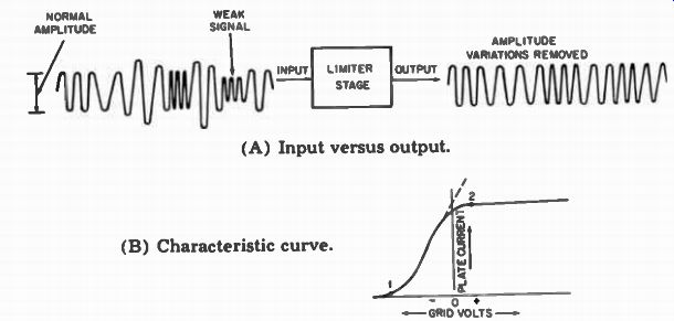
Fig. 3-11. Ideal limiter performance.
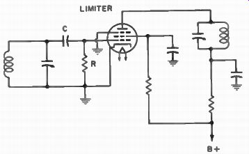
Fig. 3-12. Typical limiter stage.
A limiter is in reality an IF amplifier so arranged that, be yond a certain point, a further increase in grid signal will produce no corresponding increase in plate-current signal. If the gains in the low-IF amplifiers are such that a strong signal is delivered to the limiter, amplitude variations in the signal will be removed. Since the discriminator responds to frequency variations only, the removal of these excessive amplitude variations does not adversely affect the signal reproduction. Notice in Fig. 3-11A that the input signal to the limiter varies in amplitude as well as frequency, but that the output varies in frequency only. Also notice that weak portions of the input are amplified to the desired level. The plate and screen voltages of a limiter stage are generally lower than in a regular amplifier, and a relatively small bias is applied to the control grid. Therefore, a highly positive grid-signal voltage drives the tube quickly into saturation; conversely, a highly negative signal drives it into cutoff. Fig. 3-11B shows the transfer characteristic of the ideal limiter. Any portion of grid signal below point 1 of the curve will cut off the plate current, any portion beyond point 2 will fail to increase the plate current any further. However, any signal that does not quite swing from points 1 to 2 will be amplified. For good limiter action, the input to the limiter should therefore be between the two points.
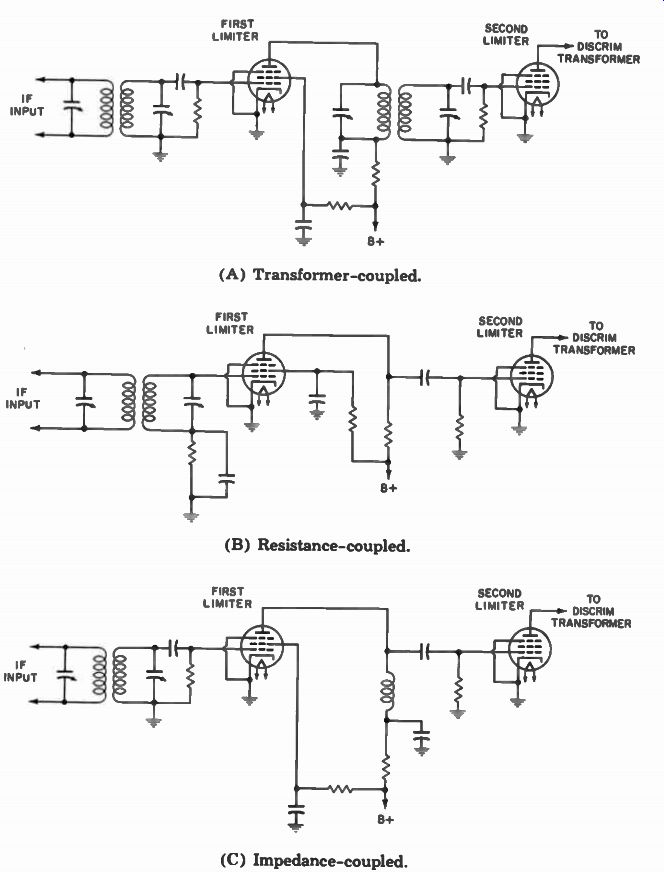
Fig. 3-13. Cascade limiters. (A) Transformer-coupled. (B) Resistance-coupled.
(C) Impedance-coupled.
Fig. 3-12 shows a limiter circuit that looks just like a typical IF amplifier except for the RC network in the grid circuit; this network provides the input clipping action on excessive noise peaks, and also furnishes the grid operating bias. This RC combination produces a voltage as a result of the peak DC rectified voltage between cathode and grid. Any noise pulses in the input signal that are longer than the time constant of the RC network are clipped off, but the longer variations caused by signal fading actually appear in the limiter output.
To overcome this fading, the normal design procedure is to follow the first limiter with a second having an input network with a longer time-constant.
Notice in Fig. 3-13A that the limiters are transformer coupled; this method provides greater gain for the second limiter, but is disadvantageous when there is sufficient signal to saturate the first limiter. The resistance-coupling method in Fig. 3-13B is more widely used because of its simplicity and ease of adjustment. The impedance coupling in Fig. 3-13C is a compromise between the two.
Any over-all gain in the limiters is undesirable because it will increase the problem of high-gain intra-stage feedback.
Amplification in the limiter takes place only when there is in sufficient signal to drive it into saturation. Since about 2 volts of signal is required to saturate the limiter, an over-all gain of 2,000,000 must be realized ahead of it with an input of 1 microvolt in the antenna.
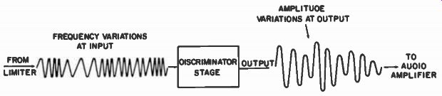
Fig. 3-14. Discriminator input versus output.
THE FM DISCRIMINATOR
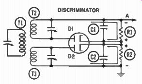
Fig. 3-15. Double-tuned discriminator circuit.
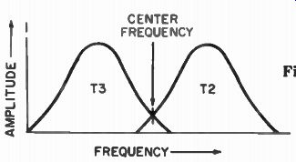
Fig. 3-16. Response of discriminator.
In FM receivers the discriminator converts the IF signal into audio. Fig. 3-14 shows the signals before and after passing through the discriminator. Notice that as the input to the discriminator varies only in frequency, the voltage (amplitude)
in its output likewise varies. When the frequency reaches a peak value on either side of the center frequency, the output (audio) voltage also reaches a peak value. . Fig. 3-15 shows a circuit of a typical double-tuned discriminator used in communications receivers. T1 is tuned to the FREQUENCY IF (center) frequency, and T2 and T3 are tuned above and below the carrier frequency (Fig. 3-16). With a constant amplitude center-frequency carrier applied across T1 in Fig. 3-15, the voltages developed across T2 and T3 will be 180 deg. out of phase, and alternate polarities will appear at the anodes of D1 and D2. These voltages will increase and decrease in amplitude with the changing frequency; for example, assume that T2 is higher in frequency than the incoming IF signal.
As the induced voltage approaches the resonant frequency of T2, its amplitude increases in a positive direction. If T3 is now tuned the same amount lower than the incoming IF, as the induced voltage approaches the resonant frequency of T3, its amplitude will increase in a negative direction. When the anode of D1 goes positive, the conduction is from the cathode, through the tube to the anode, through T2, and back through R1 to the cathode. Therefore, the resultant IR drop across R1 will be equal to the signal in T2; likewise, as the signal goes positive at the anode of D2, current will flow in the same manner. Capacitors C1 and C2 filter out any AC variations and thus permit a pure DC voltage to be developed across R1 and R2. In this manner the voltages across the individual load resistors, R1 and R2, oppose each other because both cathodes are at the same potential. Therefore, the total IR drop between the top of R1 and ground depends on the IR drops across the individual resistors. Since the voltages across the individual resistors depend on the polarity of the applied signal, if the incoming signal is higher in frequency than the resonant circuit of Ti, D1 will conduct more heavily than D2 (be cause T2 is tuned higher than the carrier). On the other hand, if the incoming signal is lower than the resonant circuit of T1, D2 will conduct more heavily (because T3 is tuned lower than the carrier). Depending on which half of the discriminator conducts more heavily, one of the resistors will have a larger IR drop across it. However, if the incoming carrier is exactly at the resonance bandpass of T1 (center frequency), the IR drops across both resistors will be equal and thus the total output voltage of the discriminator will be zero. As an example, when the incoming signal increases in frequency, more voltage is developed across T2. As a result, a greater IR drop appears across R1, thus making point A more negative.
When the signal drops below the center frequency, more voltage is developed in T3 than T2. Hence, there is a larger IR drop across R2, and point A now becomes more positive with respect to ground. As the applied frequency swings from above to below the center frequency, point A therefore goes from negative to positive; this results in the output-voltage-versus frequency curve in Fig. 3-17A. The voltage across the individual resistors, with respect to frequency, is shown in Fig. 3-17B.
(A) Across discriminator. (B) Across resistors.
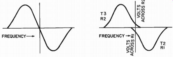
Fig. 3-17. Output voltage of discriminator.
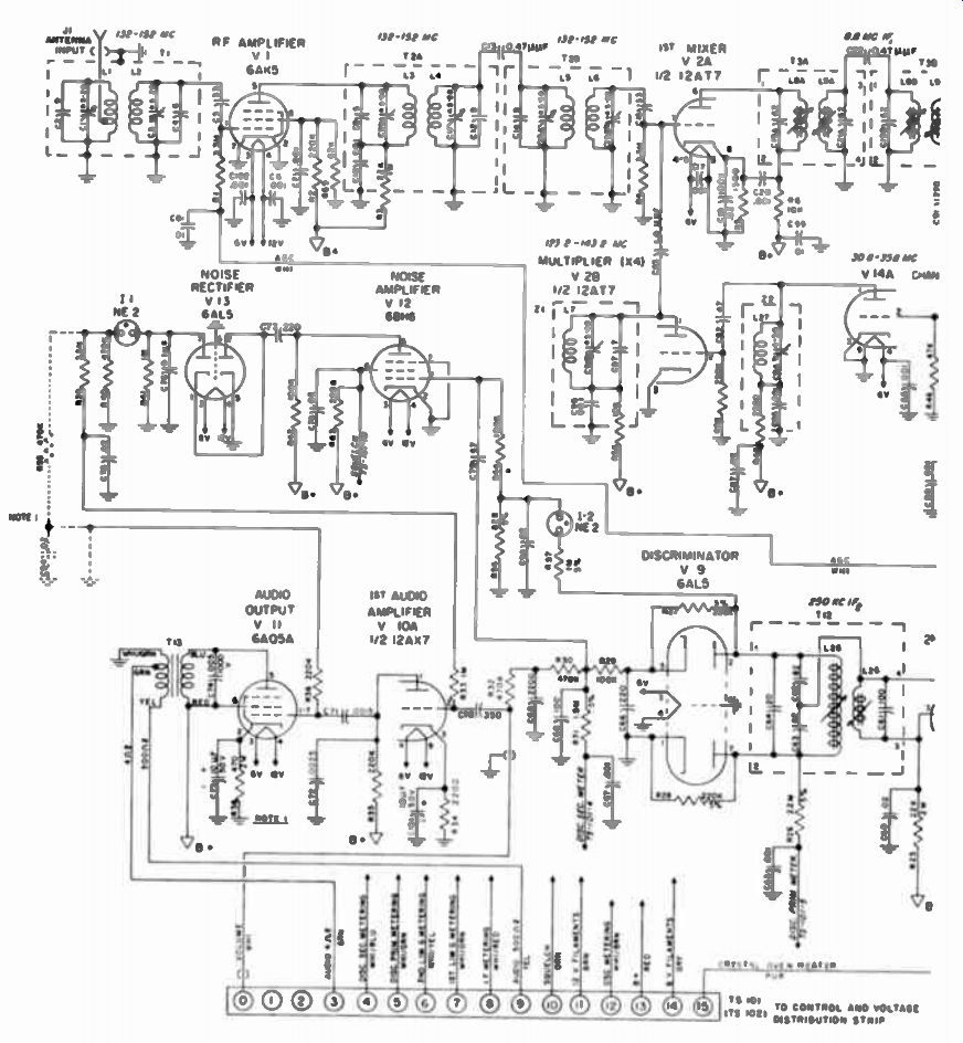
Fig. 3-18. Schematic of the Comco 400-R-E receiver.
COMCO 400-R-E RECEIVER
The receiver in Fig. 3-18 is a fixed-frequency, crystal-con trolled, dual-conversion superheterodyne type for use in mobile or fixed FM station equipment in the 144-174- mhz band. Each frequency conversion is controlled by a separate crystal. The receiver is designed for either wide- or narrow-band operation and can be easily changed from one to the other.
The Comco 400-R-E provides good sensitivity and has sufficient front-end selectivity to minimize the possibility of over-load, desensitization, intermodulation, mixing, and other un desirable conditions caused by a strong adjacent or off-channel signal. High-Q dual tuned circuits (filters) are provided between the antenna, RF stage, and first mixer.
An overtone crystal is used in the channel-determining oscillator for the first conversion. This, of course, minimizes the possibility of spurious responses. Provision is made for controlling the temperature of the channel-determining crystal.
A temperature-controlled crystal is essential for split-channel operation.
High-Q multi-tuned circuits follow the first mixer. Operating as a filter at the first IF frequency, they reject the second IF image and thus further minimize spurious responses. These circuits are followed by the second mixer/second oscillator, which uses a crystal similar to the military CR-18/U. The output of the second conversion is 250 khz. The second mixer is followed by two extremely high-Q tuned circuits, which provide the desired selectivity for the receiver. Two types are available, depending on whether the receiver is for use in wide-band (60- khz channel system with - ±15- khz deviation) or narrow-band (20- to 30- khz channel system with - ± -5- khz deviation) operation. The change from broad to sharp selectivity can be accomplished by either (1) changing the filters, or (2) changing component values and/or removing several resistors and capacitors and retuning by the peaking method.
The latter can be performed by the average technician with a standard signal generator. However, both broad- and narrow band pre-tuned filters are offered for the customer's convenience.
The front-end gain of the receiver is purposely kept low to reduce mixing, overloading, and other undesirable conditions.
The major portion of the gain is in the two 250- khz IF2 stages (V5 and V6) following the high-Q filters. These are followed by two limiters, the discriminator, the de-emphasis network, and a conventional AF system with a speaker output of approximately 2 watts. A voltage-compensated squelch circuit, associated with the limiter and audio circuit, eliminates noise during standby.
RF Amplifier
Radio-frequency signals picked up by the antenna are coupled to antenna jack J1 and then to the grid of RF amplifier V1 through a high-Q double-tuned circuit. This circuit presents the proper load impedance to match a 50-ohm antenna input. The RF amplifier (VI) obtains grid bias from contact potential developed across the grid resistor. When the grid voltage of the second IF amplifier exceeds a certain level, AGC voltage is fed to the RF-amplifier grid circuit. This voltage reduces the gain of the RF amplifier and thereby prevents intermodulation by adjacent- or alternate-channel signals. RF signals which have been amplified in V1 are then coupled, through four additional high-Q capacitor tuned RF circuits, to the grid of the first mixer (V2A). These tuned circuits consist of two capacitively coupled, double-tuned transformers, T2A and T2B. First Oscillator The first oscillator (V14A) utilizes an overtone crystal which oscillates at one-fourth the first-mixer injection frequency. (The injection frequency is always equal to the channel frequency minus 8.8 mhz.) The crystal is ground to a tolerance of - ±.0015%. It plugs into an octal-socket crystal oven using pins 2 and 8. This oscillator circuit operates the crystal on its third mode when the plate circuit (Z2) is resonated according to the tuning instructions. The use of mode-type crystals greatly reduces the possibility of spurious responses.
Crystal trimmer coil L28 is provided in series with the channel-determining crystal so that the latter can be set on the exact frequency. The trimmer can vary the injection frequency approximately ± - .006% or more. This is sufficient to compensate for the crystal-grinding tolerances, and also to permit netting into systems which are permitted channel-frequency tolerances such as -±.005%. Oscillator grid voltage is developed across resistor R46 and metered through R45. The oscillator output is coupled through capacitor C82 to the grid of V2B, where the frequency is quadrupled. The plate circuit of this stage is resonated to the multiplied frequency, and coupling capacitor C83 is used for injection to the first mixer grid. Grid bias is developed across multiplier grid resistor R59.
First Mixer of the IF1 Amplifier
The first mixer (V2A) receives the amplified RF signal and the first-oscillator multiplier output on its control grid. These are combined in the first mixer type, and the resulting difference frequency is the first IF of 8.8 mhz. This signal is then passed through four tuned circuits before being applied to the grid of 8.8- mhz IFI amplifier V3. The tuned circuits consist of transformers T3A and T3B, which utilize high-Q slug-tuned coils. Both transformers are coupled by capacitor C22.
The amplified 8.8- mhz signal in the plate circuit of IF1 amplifier V3 is coupled, by T4, to the grid of second mixer V4A, which is half of a 12AT7 tube.
Second Oscillator
The second crystal oscillator is operated at 8,550 khz. Its plate circuit is coupled to the second-mixer control grid through injection capacitor C89.
Second Mixer
The 8.8-me IF signal and the second-oscillator output of 8,550 khz are coupled to the control grid of second mixer V4A, and are combined in the tube to form the desired difference frequency of 250 khz. The second mixer and second oscillator are both in the same tube (V4), a dual triode 12AT7.
First IF2 Amplifier
The second-mixer output of 250 khz is coupled through the high-Q tuned-circuit transformers, which provide the basic selectivity for the receiver. Each transformer utilizes different amounts of coupling to obtain the desired selectivity. however, the coupling of these coils can be changed (as outlined in the tuning procedure) in order to convert the receiver selectivity from broad- to narrow-band.
After passing through T5, T6, and T7, the 250- khz IF., frequency is amplified by the first IF., amplifier (V5). It then passes through T8, T9, and T10, to the grid of second IF., amplifier V6. Drive to the grid of the second IF2 amplifier is metered through resistor R15. The signal is amplified in the second IF amplifier. It then passes through another double tuned IF transformer (T11) which, because of its very high impedance, gives extremely high gain from the second IF2 amplifier.
Discriminator
The output of second limiter V8 is fed to a Foster-Seeley type of discriminator which has a high output and good linearity. The discriminator transformer has temperature compensation (provided by capacitor C64), and has been impregnated with a high-temperature wax to protect it from moisture. The discriminator is therefore extremely stable with temperature and humidity changes (and is also unaffected by shock and vibration). Its output (pin 5, V9) contains the audio (or noise, in the absence of a signal).
Noise Amplifier and Squelch Circuit
The discriminator output, in the absence of a signal, consists of amplified thermal or shot noise (among other things), which originates in the early stages of the receiver. This noise then passes through RF filter network R29-C68 and is impressed on the noise-amplifier grid through coupling capacitor C79. It is then amplified through noise-amplifier tube V12, the gain of which is controlled by turning the Squelch control (on the control panel) to raise or lower the screen voltage. The amplified noise in the plate circuit is coupled, through capacitor C77, to the plate of noise rectifier V13, which functions as a voltage doubler.
This voltage is filtered by C76, which has sufficient capacitance to remove most noise fluctuations. The rectified noise voltage is then applied to the NE-2 neon bulb l1. With no input signal to the receiver and with the Squelch control advanced to the point where the V12 screen voltage has increased so that approximately -70VDC is across capacitor C76, bulb l1 will have sufficient voltage to ionize (and hence conduct). A negative DC voltage will then pass through RF filter R39, and C75 will have sufficient amplitude to completely bias first audio amplifier V10A beyond cutoff. When the latter occurs, there will be no audio output from the receiver. A negative DC voltage may also pass through R55 and R36 to the grid of audio-output tube V11, depending on the wiring of the receiver. From the schematic you can see that C94, R36, and R55 may be connected to the neon-bulb output or that R36 may be connected to ground. If the screen voltage on noise amplifier V12 is reduced with the Squelch control, the voltage across C76 will be reduced below the ionization (conduction) point of the neon bulb. When this occurs, the bias voltage-measured from the control grid of first audio amplifier V10A to ground- will disappear. The neon bulb provides a positive and very fast acting squelch action. As a signal is received, the bias increases on the limiter control grids, thereby reducing their gain. In turn, less "thermal" or "shot" noise is applied to the noise amplifier. When the noise amplifier and rectifier receive less noise, the voltage presented to the neon bulb (l1) will be too low to cause conduction. As a result, no negative voltage will be applied to first audio amplifier V10A. Being unbiased, the tube will therefore amplify the signal.
If R55, C94, and R36 are connected to l1, the negative squelch voltage will be applied to the grid of audio-output tube V11 and partially cut it off while the squelch is operating.
This bias reduces the battery drain and also permits inserting a 300- to 500-ohm squelch relay in place of the cathode resistor.
This relay, which must have suitable sensitivity in order to operate, can be used for signaling or for operating other devices. If resistor R36 is connected to ground, the audio-output tube will not receive the extra bias while the receiver is "squelched off." The squelch operation is slightly better when the audio-output stage is not receiving this extra bias; there fore, it is suggested that resistor R36 be connected to ground except when a squelch-operated relay is desired. The squelch circuit in this receiver has a means of compensation, to pre vent power-source voltage variations from opening or tightening the squelch.
Compensation is obtained by coupling the negative voltage from the discriminator plate, through a neon bulb and a resistive voltage divider, to the grid return of the noise amplifier.
The neon bulb, having a constant voltage drop, will supply to the noise amplifier a bias with a greater percentage change than the voltage present at the discriminator plate. The bias voltage changes the gain of the noise amplifier so that its output is held constant. Of course, the noise-amplifier voltage output can still be adjusted with the Squelch control. When set at its most sensitive point, the squelch will operate with signals that provide approximately 2 db of noise quieting in the receiver audio output. The Squelch control should be adjusted to a point just beyond where slight pulses of noise are heard in the speaker. If advanced any further, the squelch will require stronger signals in order to operate.
After going through RF filters R29 and C68, the discriminator output is passed through de-emphasis network R30-C69.
This network-in combination with other tone-compensating capacitors such as C70, C72, and C74-results in an audio response which has a decreasing 6-db-per-octave slope from 300 to 3,000 cycles without deviating from a tube 6-db-per-octave de-emphasis slope by more than +2 to -8 db. From the de emphasis network the audio signal is applied through capacitor C70 to first audio amplifier V10A, which derives its operating grid bias from cathode resistor R34. Here the audio signal is amplified and then applied, through coupling capacitor C71, to the grid of audio-output stage V11. Correct operating grid bias is obtained for V11 by means of its cathode resistor, R38, which is bypassed by electrolytic capacitor C73. The audio output from the plate of V11 is coupled to transformer T13 (which has two secondary output impedances, 4 ohms and 500 ohms). Capacitor C74, across its primary, controls the audio-frequency response and also protects transformer T13 from high-voltage audio surges.
Also see: