The video channel consists of the stages from the tuner to the picture tube-the video IF amplifier, video detector, and the video amplifier. These circuits amplify and process the video signal for application to the picture tube to reproduce the picture.
VIDEO IF AMPLIFIERS
The television receiver is a high-frequency superheterodyne; most of the gain is contributed by the IF amplifiers. IF stage gain is measured as shown in Fig. 9-1. Recall that there are actually two IF signals at the mixer output: the video IF and the sound IF. These two frequencies are separated by the 4.5-MHz difference set by the transmitter. The response of the IF amplifiers is made wide enough that both frequencies are passed. In the video detector, the sound IF and video IF are beat together to produce the 4.5-MHz-intercarrier sound signal.
In early television receivers the sound and video IF signals were separated directly at the mixer output, and separate IF amplifiers were employed for the video and sound. This method was called split sound; however, it is not employed in any modern receivers. All modern receivers use the intercarrier principle.
IF Requirements
The requirements of the television IF amplifier system are far more complex than the IF amplifiers in broadcast receivers. In broadcast receivers, the IF amplifiers must pass a band of frequencies only 10 kHz wide. In FM receivers, the bandwidth requirements are only 200 kHz. In a television receiver, however, the IF amplifier must pass a band of frequencies 5 MHz wide. In addition to the requirement of passing the wide band of frequencies, other frequencies must be attenuated so that they cannot cause interference in the desired channel. These frequencies are:
1. Sound carrier of the adjacent lower channel
2. Video carrier with its modulation in the next higher adjacent channel
In addition, the sound IF of the desired channel must be reduced to a level 23 to 26 db below the video carrier within the IF amplifier system. If the sound carrier is not reduced, sound bars (interference) will appear in the picture. Figure 9-2 shows the basic IF and VHF frequency relations.
The number of stages of amplification varies among the different manufacturers and the intended application of the receiver (fringe or local reception). Sets with only one IF amplifier or as many as five stages have been produced. Most receivers, however, employ two or three stages of IF amplification.
In Section 8 it was stated that the use of 45.75 MHz as the video IF and 41.25 MHz for the sound IF was practically universal in modern receivers. Formerly, many other frequencies were used as the sound IF. Some of them are as follows:
Video IF Carrier, MHz
Sound IF Carrier, MHz
15.2 10.7 229 27.4 25 75 21.25 26.1 21.6 262 21.7 264 21.9 26 25 21.75 266 22.1 26 75 22.25 373 32.8
Video IF Response Recall that in vestigial sideband transmissions (Fig. 9-3A), the amplitude of the transmitted signal is practically constant from approximately 0.75 MHz below the video carrier to 4.0 MHz above the carrier. Also, between 0.75 and 1.25 MHz below the carrier, a portion of the lower sideband is transmitted. Thus, if such a carrier and its sidebands were to be applied to a linear detector, the output would be as pictured in Fig. 9-3B. Obviously, such an output would not give the desired results. With the response of Fig. 9-3B, all objects that result in a video frequency up to 0.75 MHz from the carrier would receive twice the amplification as those from 1.25 to 4.0 MHz. Between 0.75 and 1.25 MHz, the response tapers gradually from 100 to 50 percent.
Some method of compensating for the increased low frequencies due to the double-sideband transmission must be provided in the video IF amplifier. This compensation is provided by reducing the amplification at the carrier frequency and increasing it at the higher frequencies. Thus, the ideal video response should appear as shown by curve B in Fig. 9-4; curve A shows the trans mitted carrier.
In curve B, the video carrier is set at the 50 percent point, and the areas between 0.75 MHz above and below the carrier are less than 100 percent of the response. However, by adding the portion of the response between 0.75 MHz below the carrier and the carrier to the response between the carrier and 0.75 MHz above the carrier, the curve at D will result. Thus, these two portions of the curve, when added together, result in an overall 100 percent response between the carrier and the 0.75-MHz point.
It is impossible to obtain the straight-line response of curve B in Fig. 9-4. Notice, however, the curve at C will also add to the desired response. At the high-frequency end of the response, the ideal curve is depicted by curves A and B. Usually, however, the high-frequency response is tapered off, as shown by curves C and D. This tapering off at the high-frequency end does reduce the fine details in the picture, but it is not noticeable in the aver age scene. In practice, few receivers provide more than a 3.0 MHz response.
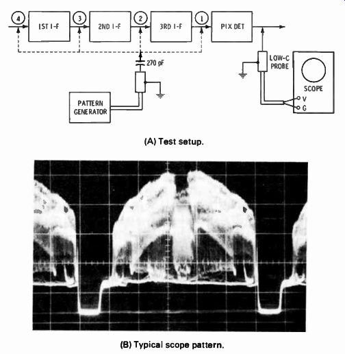
Fig. 9-1. Measurement of IF stage gain. (A) Test setup; (B) Typical scope pattern.
Fig. 9-2. IF and VHF frequency relations.
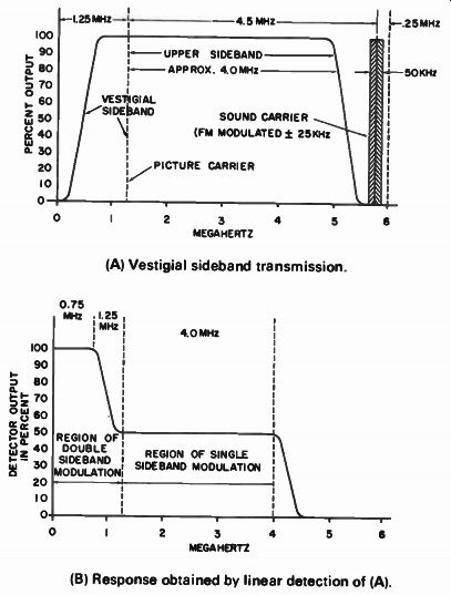
Fig. 9-3. Effect of linear detection of the carrier. (A) Vestigial sideband
transmission. (B) Response obtained by linear detection of (A)
Up to this point, we have discussed the frequencies as they are transmitted; that is, the video carrier in Figs. 9-3 and 9-4 is shown at the low end of the response curve, and the sound carrier is shown at the high end. Recall, however, that the receiver local oscillator frequency is higher than the transmitted carrier frequency; therefore, in the IF amplifiers, the sound IF will be located at the low end of the response curve, and the video IF will be at the high-frequency end. Also, in an actual receiver, the ideal response of Fig. 9-4 is seldom obtained. The actual response of the IF amplifier section will usually appear similar to the curve of Fig. 9-5.
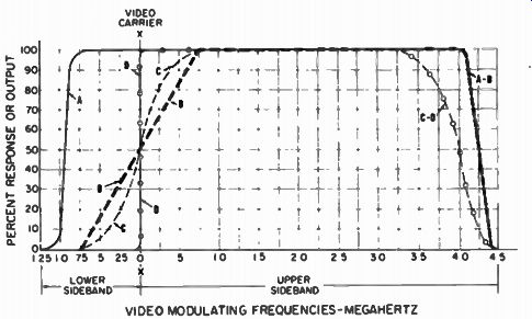
Fig. 9-4. Overall receiver characteristic required to compensate for vestigial
sideband modulation.
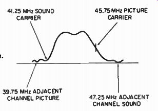
Fig. 9-5. Typical video IF response.
IF Traps
In addition to providing amplification of the desired frequencies, the video IF amplifiers must also prevent certain undesired frequencies from being amplified and passed on to the following stages. This function is performed by trap circuits in the IF amplifier stages.
Based on the 41.25- and 45.75-MHz sound and video IF frequencies, traps are usually included for the following frequencies.
1. 39.75 MHz adjacent-channel sound carrier
2. 41.25-MHz co-channel (desired) sound carrier
3. 45.75-MHz adjacent-channel video carrier
Two types of traps are employed: shunt and absorption traps. The shunt trap (Fig. 9-6) consists of a series-resonant tank connected in shunt (parallel) with the input circuit. This circuit presents a low impedance to any signals at the resonant frequency of the coil and capacitor. Thus, any signals at these frequencies will be shunted to ground. The adjustment of the coil permits precise adjustment of the trap to the desired frequency.
Either the coil or the capacitor can be made adjustable; however, in actual practice, the coil is usually made adjustable, as shown in Fig. 9-6.
The absorption trap (Fig. 9-7) consists of a parallel-resonant circuit inductively coupled to the IF transformer. At the resonant frequency, maximum current flows in the trap circuit. This current must be absorbed from the IF transformer; therefore, any current at the trap resonant frequency present in the IF trans former secondary will be removed.
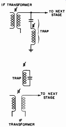
Fig. 9-6. Shunt trap.

Fig. 9-7. Absorption trap.
IF Amplifier Circuits
As mentioned previously, the IF amplifier circuit must be cap able of passing a wide band of frequencies. The video modulation extends approximately 4 MHz from the carrier. In addition, the sound IF carrier, located 4.5 MHz from the video carrier, must be passed.
The sound IF carrier, however, must not be allowed to receive the same amount of amplification as the video carrier if the circuit is to function properly. Usually, the amplitude at the sound IF frequency should be approximately 10 percent of the peak level. For this reason, traps tuned to the sound IF frequency are usually included in the video IF circuit to reduce the sound IF frequencies.
An ordinary amplifier stage would be unable to amplify the wide band of frequencies necessary in the IF system. Therefore, some means must be employed to increase the bandwidth. The following basic circuits are used for video IF amplifiers:
1. Overcoupled amplifiers (see Fig. 9-8)
2. Stagger-tuned amplifiers (see Fig. 9-9)
Stagger-Tuned IF System
In the stagger-tuned IF system, each IF stage is tuned to a different frequency in the passband. Figure 9-9 shows the effect of stagger tuning. Two stages are tuned to two separate frequencies. The response curves of the two individual stages are indicated by the solid lines in Fig. 9-9; however, the overall response of the two stages is indicated by the dotted line. Thus, by proper choice of frequencies and circuits, the response can be widened to obtain the desired response.
Figure 9-10 depicts a basic transistor IF amplifier configuration. The third IF transistor operates at higher power than the first two because the video detector requires appreciable power input. Transistor Q25 operates with a collector voltage of approximately 15 volts and an emitter current of about 15 mA. The collector-load impedance is nominally 1,000 ohms; however, transformer T8 provides some step-up voltage for the video detector. The power gain of this stage is about 18 db. It is neutralized by a 1.5 if capacitor connected from the base of Q25 to the secondary of the collector output transformer.
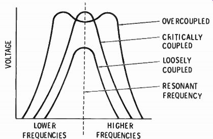
Fig. 9-8. Examples of loose coupling, critical coupling and overcoupling.
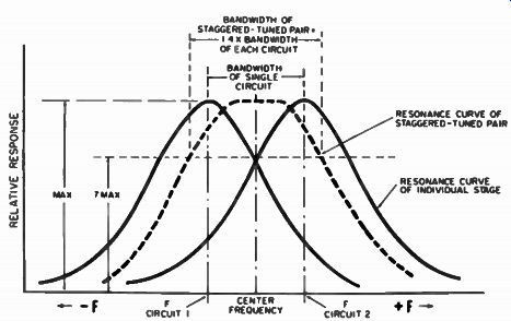
Fig. 9-9. Effect of staggered tuning.
The first stage in Fig. 9-10 operates at 15 volts on the collector and an emitter current of 4 mA. Reverse AGC is applied to the base of Q27; this is conventional AGC action in which the transistor is AGC-biased toward cutoff. The minimum collector current of Q27 under strong-signal conditions is approximately 50 µA. Q27 has a dynamic range of 40 db. Diode D12 is a clamp diode that becomes reverse-biased to prevent Q27 from being completely cut off when the AGC voltage reduces the RF tuner gain to a very low value. Q27 is neutralized by the 1.5-µf capacitor connected from its base to T6.
Two traps are connected into the input circuit of Q27 in Fig. 9-10: The first is an inductively coupled trap, and the second is a bridged-T configuration. These are the accompanying- and adjacent-sound traps, respectively. The collector load for Q27 is a simple resonant circuit, with a tap to provide an out-of-phase neutralizing signal. Transistor Q26 is base-driven via capacitance coupling. This second stage is not AGC-controlled and operates continuously at maximum gain. The base bias circuit for Q26 provides some negative feedback, which assists in obtaining a properly shaped IF response curve. The collector for Q26 is a bifilar transformer.
Preliminary analysis of IF trouble symptoms requires tests to isolate the defect to a particular stage. This can be done either by signal tracing or by signal substitution. Signal tracing is accomplished by means of an oscilloscope with a demodulator probe. In turn, the progress of the TV signal is checked, stage by stage, through the IF amplifier.
The chief disadvantage of the signal-tracing technique is that heavy loading is imposed on the IF stages by the demodulator probe. In turn, the results of a signal-tracing test are not always conclusive. For this reason, many technicians prefer a signal substitution procedure, such as outlined in Fig. 9-11. A generator is used as a signal source, and the picture tube serves as an indicator.
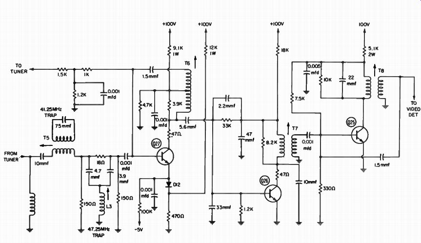
Fig. 9-10.
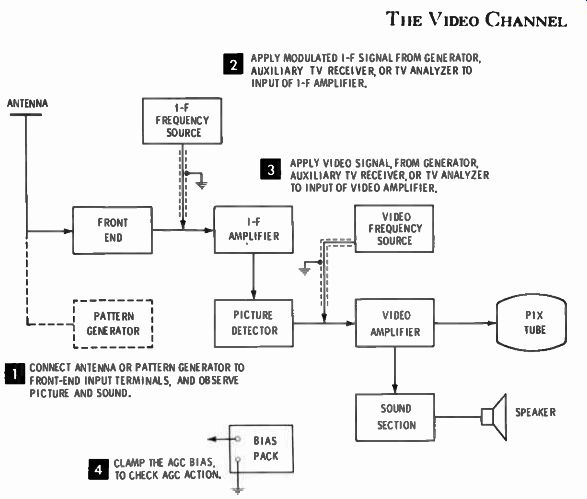
Fig. 9-11. Pointers for isolating defect of IF strip.
VIDEO DETECTORS
The video IF amplifier is followed by the video detector, which is essentially the same as the second detector in AM broad cast or short-wave radio receivers. However, two significant circuit differences in the TV video detector must be taken into consideration: (1) a means of compensation must be used to pre vent the loss of the higher video frequencies; and (2) the polarity of the detector output must be considered.
The video signal may be applied to the grid or to the cathode of the picture tube. To what element the signal is applied and the number of amplifiers between the detector and the picture tube determine the polarity of the detector-output signal. If there is an even number of video-amplifying stages between the detector and the picture-tube grid, the detector output must be negative going. In other words, an increase in IF carrier strength at the detector results in a more negative video signal with respect to ground. Figure 9-12A shows a detector that supplies a negative picture polarity.
If an odd number of video-amplifying stages are employed (in most instances, this will be a single stage) and the video signal is applied to the grid of the picture tube, the detector must be connected as shown in Fig. 9-12B. This circuit, with the plate of the diode connected to the high side of the video coupling circuit, produces a video output that becomes more positive as the video-carrier strength is increased. Figure 9-13 shows diode polarity identifications.
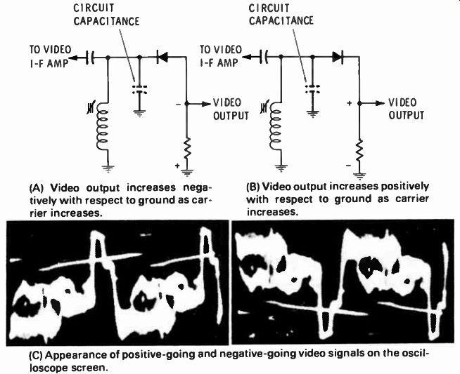
Fig. 9-12. Diode video-detector-output polarity. (A) Video output increases negatively
with respect to ground as carrier increases. (B) Video output increases positively
with respect to ground as carrier increases. (C) Appearance of positive-going
and negative-going video signals on the oscilloscope screen.
VIDEO AMPLIFIERS
The output of the video detector seldom exceeds a few volts.
Since the picture tube requires a grid swing of approximately 40 volts for its range of black to white, the signal from the video detector must be amplified through one or more stages of video amplification.
In our study of the nature of the video modulating signal, we have seen that the range of frequencies extends from 30 to over 4 million Hz/sec. For an amplifier to provide uniform gain over this extended band, compensating circuits must be used. The basic circuit, to which correction networks are applied, is the familiar resistance- and capacitance-coupled audio amplifier.
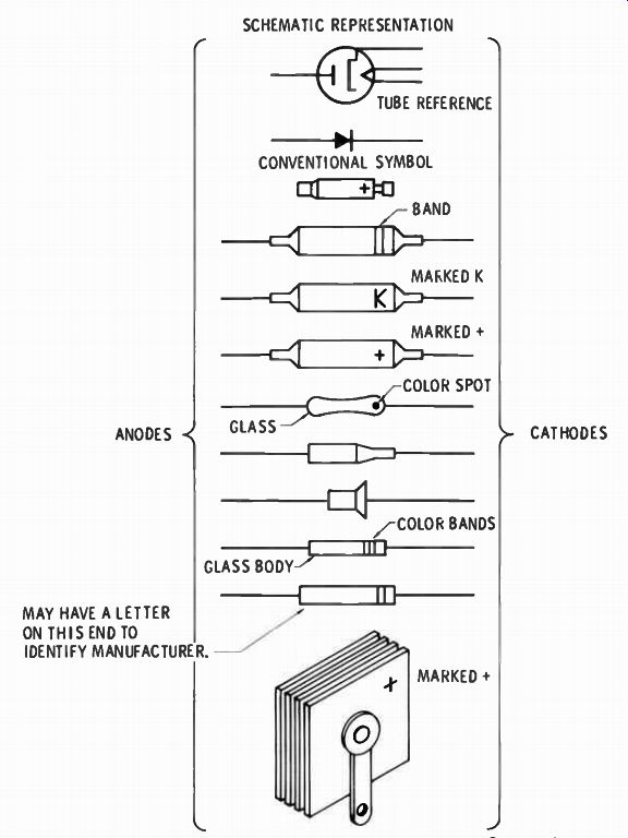
Fig. 9-13. Diode polarity identifications.
Three separate methods of extending the range of a resistance and capacitance-coupled amplifier for video use are:
1. Low values of collector load or coupling resistance
2. Low-frequency compensation to overcome effects of coupling network, unless direct coupling is used
3. High-frequency compensation to overcome effects of total circuit capacitance
Low Value of Collector Load
Figure 9-14 shows the effect of changing the value of the collector-load resistor. The band of video frequencies over which the output is flat is greatly extended as the coupling resistance is decreased. The choice of load resistor is a compromise between bandwidth and gain. The voltage gain of a video stage is seldom more than 20, whereas in resistance-coupled audio stages gains of as high as 150 are possible. Load resistors of 2,000 to 4,000 ohms are common in video amplifiers. After the value of load resistance is determined, the stage is compensated to raise the gain at frequencies below approximately 100 cycles and above several hundred kilohertz. If direct coupling is used, no LF compensation is required.
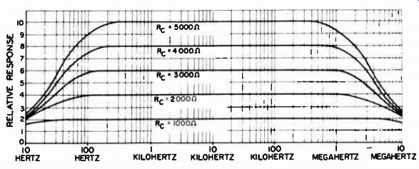
Fig. 9-14. Effect of plate load resistor on gain and bandwidth.
A typical transistor video amplifier is depicted in Fig. 9-15; this amplifier has a nominal gain of 28 db. The video-drive transistor Q204 is connected as an emitter-follower in order to match the comparatively high impedance of the video detector to the input impedance of the video-output transistor Q205. The contrast control is the emitter resistance for the video-driver stage. A 4 -uf coupling capacitance is required to obtain good low-frequency response because this capacitor works into a 10-ohm resistance.
An NPN transistor, especially designed to handle a large amplitude signal, is used in the video-output stage.
The output-signal voltage provided by the video amplifier in Fig. 9-15 ranges from 25 to 50 volts peak to peak. Note that the collector of the video-output transistor is returned to a 140-volt power supply. With the contrast control turned to maximum, an output-signal amplitude of 100 volts peak to peak can be provided. A light-dependent resistor (LDR201) is used to automatically vary the picture contrast and brightness as the ambient room lighting varies. This device acts to increase or decrease the gain of the video amplifier, thereby automatically controlling the contrast. Since the collector of Q205 is dc-coupled to the cathode of the picture tube, the brightness is also controlled automatically.
Preliminary analysis of trouble symptoms in the video amplifier section is generally made with an oscilloscope, as depicted in Fig. 9-16. Waveforms are checked for amplitude (peak-to-peak voltage value) and for distortion. Instead of making a frequency-response check, a square-wave test may be used.
If a video amplifier is in normal operating condition, it will pass a 100-kHz square wave without substantial distortion.
Measurement of de voltage and resistance values are basic in pinpointing defective components. These tests apply to solid state video amplifiers, as well as to tube-type amplifiers. Note that receiver service data often provide resistance charts to facilitate in-circuit resistance measurements. A typical chart is shown in Fig. 9-17. In the case of a solid-state receiver, in-circuit resistance measurements should be made with an ohmmeter that applies less than 0.08 volt across points under test, as noted in the chart.
A "hi/lo-pwr" ohmmeter is provided in the electrical multimeter shown in Fig. 9-18. The advantage of a lo-pwr ohmmeter in solid-state troubleshooting is that normal semiconductor junctions will not be "turned on" during in-circuit resistance measurements. A "turned-on" junction represents an unexpected shunt-resistance path that makes the resistance measure virtually meaningless.
Fig. 9-15. Transistor video-amplifier circuit
Fig. 9-16. Troubleshooting procedure for preliminary analysis of video amplifier malfunctions.
Fig. 9-17. Resistance measurements.
BRIGHTNESS CONTROL
At several points, we have indicated that the variation of video, or picture, signal on the control grid of the picture tube is responsible for the instantaneous changes of spot illumination that makes up the elements of the picture. When the signal voltage on this control element changes in a negative direction, a darker spot is produced on the screen. Finally, at some critical negative voltage, the spot of light is entirely extinguished.
One of the essential controls of the television receiver is a bias adjustment on the grid. This adjustment ensures that the blanking level, or pedestal, of the signal occurs at the black point. Figure 9-19 shows two bias systems in which the voltage established by adjustment of the brightness control biases the control grid with respect to the cathode and determines the correct picture brightness. Because of the polarity of the video signal in Fig. 9-19A, the signal from the plate of the video-output tube is connected to the control grid of the picture tube.
Figure 9-19B shows the video signal applied to the cathode of the picture tube. In either case, the brightness control is a voltage adjustment of the bias between the control grid and cathode, and it establishes the correct blanking or black level.
Fig. 9-18. Electronic multimeter, which provides "hi-power" and "low power" ohmmeter functions.
(A) Video signal applied to grid. (B) Video signal applied to cathode.
Fig. 9-19. Brightness-control circuits.
Fig 9-20. Basic integrated circuit configuration.
Fig. 9-21. Configuration of an integrated IF amplifier stage.
Fig. 9-22. Integrated IF circuit showing connections to external components.
INTEGRATED CIRCUITS Integrated circuits (ICs) are now used to a greater extent than previously in RF and IF amplifiers. Most IC units are based on the differential-amplifier configuration shown in Fig. 9-20. The transistors are formed in a single chip: Q1 and Q2 are called a differential pair; Q3 is termed a constant-current sink. Adjustment of the base voltage VB3 determines the current I c3 and, in turn, the operating voltage of the amplifier circuit. The total collector current I c3 branches through QI and Q2 in accordance with the applied voltages VIII and VB2. Use of a differential pair makes the amplifier relatively free from effects of temperature changes.
With reference to Fig. 9-21, QI operates in a common-emitter configuration with the IF signal applied to the base. In turn, QI drives Q2 and Q3, which operate in a common-base configuration called a cascode pair. It employs a pair of transistors connected in series. The collector of Q3 is effectively grounded, and the IF signal output is taken from the collector of Q2. Diode DI provides delayed AGC; the AGC voltage varies over a range of approximately 0.86 volt in normal operation. In this example, if the AGC voltage exceeds the nominal base voltage on Q2 by 57 mV, Q2 will be cut off and the collector current will be confined to QI and Q3. Since Q2 is cut off, the stage gain is minimum under this condition of AGC voltage.
Next, if the AGC is less than the nominal base voltage by at least 57 mV in Fig. 9-21, all the collector current from QI will pass into the emitter of Q2; Q3 is biased to cutoff. In turn, Q2 develops an amount of gain that depends on the particular value of applied AGC voltage. A supply voltage of 20 volts is used in this example and is applied to terminal 6, as shown in Fig. 9-22.
Terminals 8 and 10 are bypassed to ground with 0.005-uf capacitors; terminals 2 and 3 are connected to ground via 11-ohm resistors. The substrate, terminal 7, is grounded. Ordinary slug-tuned coils and capacitors are used to couple one IC to the next.
Fig. 9-23. Module for a TV receiver.
Fig. 9-24. Layout of typical modularized TV receiver.
MODULAR CONSTRUCTION
Various receiver designs include modular construction. A module, such as the one shown in Fig. 9-23, is similar to a printed circuit board, except that it is designed to plug into the receiver.
It can be unplugged, in turn, without any disconnection of leads.
Modular construction facilitates troubleshooting procedures because a known good module can be quickly substituted for a suspected module. In turn, if normal operation is restored, the defective module can be repaired at any convenient time.
Some receivers are extensively modularized, as shown in Fig. 9-24. However, there are always a few chassis-mounted components. For example, the VHF and UHF tuners and the power transformer are always chassis-mounted.
TURN-OFF AND TURN-ON TESTS
If a transistor is suspected of being defective, it is frequently possible to make in-circuit turn- off and turn- on tests to determine whether the transistor is workable. These are quick checks that provide basic go/no-go answers.
With reference to Fig. 9-25, a turn-off test is made in this type of circuit by measuring the collector-emitter voltage and then applying a base-emitter short circuit to observe any change. If the transistor has normal control action, the voltmeter indication jumps up to the collector supply-voltage value when the short circuit is applied. Otherwise, the transistor is defective and it should be unsoldered from its circuit and replaced.
Next, a turn-on test is made by temporarily connecting a 10 ohm resistor between the collector and base terminals of the transistor. A de voltmeter is connected across the emitter resistor in the type of circuit. If the transistor has normal control action, the voltmeter indication will increase substantially when the for ward bias is increased. Otherwise, the transistor is defective and should be unsoldered and replaced.
Fig. 9-25. Basic in-circuit turn-off and turn-on transistor tests.
(A) Turn-off test in a two-battery circuit.
(B) Turn-on test in a one-battery circuit.
(C) Turn-on test in a one-battery circuit.
SUMMARY
In early television days the sound and video IF signals were separated directly at the mixer output, and separate IF amplifiers were used for the video and sound. This method, called split sound, is not used in modern receivers. All receivers use the inter carrier system, which is a receiver that uses the picture carrier and associated sound-channel carrier to produce an intermediate frequency equal to the difference between the two carrier frequencies. This intermediate frequency is frequency-modulated in accordance with the sound signal.
The requirements of the television IF amplifier system are far more complex than the IF amplifiers in broadcast receivers. In broadcast receivers, the IF amplifier must pass a band of frequencies only 10 kHz wide. FM receivers have a bandwidth of 200 kHz. In television receivers, the IF amplifier must pass a band of frequencies 5 MHz wide.
Vestigial sideband is an amplitude-modulated transmission in which a portion of one sideband has been largely suppressed by a transducer having a gradual cutoff in the neighborhood of the carrier frequency.
QUIZ
1. What frequencies must the IF amplifier pass in AM receivers? FM receivers? TV receivers?
2. What are the video IF and sound IF frequencies used in modern TV receivers?
3. Explain vestigial sideband transmission.
4. What is the purpose of using IF traps?
5. What is the advantage of a "lo-pwr" ohmmeter?
6. How does a module differ from a printed circuit board?