Discover the "right" combination when you pair this head amplifier with a low output, low impedance cartridge.
Like so many others, I was heavily involved in evaluating a number of different amplifiers, cartridges, and speakers in the "classical" analog period of the late 1970s and early 1980s. My experience was that every now and then you came across a component or unit that just seemed "right." Others prompted a niggling desire to keep adjusting levels or tweaking some other aspect of their operation, but with the "right" components or combination of components, you tended to simply sit back and listen to the music.
This was the case with the head amplifier described here when used in combination with a Fidelity Research FR1 MkIII moving coil cartridge (with the one exception of replacing the first stage transistors to reduce the amplifier noise even further). It continues to give rock solid bass, beautifully detailed, three dimensional midrange and open and effortless highs. I have not yet found a moving magnet or CD source that can equal the drama and engagement with the music.
Indeed, of the cartridges I have heard, my listening preference always tends to ward cartridges from manufacturers such as Koetsu, Linn, and the high-end Ortofon range. These cartridges lie at the very low output end of the MC range where outputs are typically only 0.1-0.2mV at 5cm/sec and impedances are typically less than 10-Ohm. As I mentioned, my favorite remains the now-scarce Fidelity Research FR1 MkIII, which has a very low output around 90µV and impedance of 1 Ohm.
Having quite a low input impedance of around 8 to 20-Ohm (depending upon the actual component values used), the head amplifier described here is best suited to the very low output, low impedance cartridges from manufacturers such as Koetsu, Linn, Lyra, Ortofon (high-end), Audionote/Kondo, and collector items such as Fidelity Research. It might not give optimal performance with higher impedance cartridges (above around 10-Ohm), and, depending upon how high their inductance is, the low input impedance might even lead to some high frequency loss with such units. With its low output impedance, you can, of course, use it in conjunction with either valve or semiconductor-based RIAA equalization stages.
The rest of my system comes largely from that classic period and includes:
• SME 3009 Series II tonearm with FD200 fluid damper
• ADC UH-MG1 Magnesium head shell
• Thorens TD124 Type II turntable
• RIAA equalization stage based upon the discrete op-amp design
• Three-way active crossover, tri-amped into a four horn system, the crucial mid/ upper range power amp being valve (push pull ultralinear 6L6 monoblocks) with a passive crossover to Decca-London ribbon tweeters.
MOVING COIL (MC) CARTRIDGES
Moving coil (MC) cartridges differ from their moving magnet (MM) counter parts in that their output impedance is very low, typically < 50-O, and their output voltage is similarly quite low, typically only around 0.1-0.5mV at 5cm/sec.
There are higher output versions, though I have yet to find one that passed the "right" test.
While the low output voltage and impedance introduces some challenges for the following amplifier stages, there are some benefits as well. The main one is that, unlike their MM counterparts, the low source impedance is capable of driving considerable cable and input capacitance without any degradation of the signal. With MM cartridges that typically have a resistance of around 500-2k-O in series with an inductance of 500-1000mH, the cable and input capacitance can lead to some unwanted frequency aberrations.
However, on the downside, with the low impedances involved, the cables and plugs must be high quality and offer the lowest possible electrical resistance. Furthermore, because the output signal of a MC cartridge may be up to 40dB below a MM (which is typically around 5mV at 5cm/sec), some form of matching to the following RIAA equalization stage is required to maintain an acceptable signal-to-noise ratio. One approach (which should not be dismissed out-of-hand) is to use a step-up transformer, though good ones tend to be quite expensive.
The alternative is to use a head amplifier to provide the required 20-40dB gain, provided that it has been designed so that it doesn't degrade the noise performance or introduce any distortion products.
NOISE IN PICKUP CARTRIDGES
The major source of noise in the cartridge is Johnson noise due to thermal motion of electrons in the resistive component of its impedance3. The root mean thermal noise voltage Nv is then given by:
Nv = v (4kTRB) volts
where k = Boltzmann's constant (1.38 × 10^-23 J/K) B = bandwidth (Hz) R = resistance (ohms) T = absolute temperature (300k at room temp) If you take B to be 20kHz (the full audio bandwidth with brick-wall cutoff ) and 3-O as the DC resistance of a typical low impedance cartridge, the thermal noise voltage is then 31.7nV.
Because of different ways of specifying bandwidth (slope of cutoff and so on), it is also common to quote the noise voltage per square root of bandwidth to give "volts per √Hertz." For the above values, this becomes 0.22nV per √Hertz.
Sometimes this is measured in relation to a power of 1mW into 600-O (i.e., 0.775V) and quoted as dBu. For this example, the 31.7nV equivalent is then -147.7dBu.
In terms of signal-to-noise, a 3-Ohm MC cartridge typically has an output of around 200µV at a recorded velocity of 5cm/sec, giving a S/N of 76dB with respect to that reference velocity (before RIAA equalization). The situation for a MM cartridge is more complicated due to the large inductive component of its output impedance. This means that its impedance at high frequencies is actually quite high, and most noise then comes from the preamp, which must have an input impedance of around 47k-O to properly load the cartridge. The thermal noise voltage from such a resistor is around 3900nV-much higher than that of the cartridge itself! A detailed analysis4 shows that the "noise" equivalent impedance of a MM cartridge over the audio bandwidth is around 12k-O, which appears in parallel with the 47k input resistor, giving a thermal noise of around 990nV. Taking this as the figure for a MM cartridge leads to an overall S/N of 74dB, in the same range as for MC cartridges.
These figures will be higher after RIAA equalization (and A-weighting, if used for the specification) due to their effect of decreasing the noise bandwidth.
Furthermore, the relatively high inductance of MM cartridges will also modify the noise spectral density affecting the comparison3,5,6. For example, Self 5 calculated the S/N for a Shure M75ED (610-O, 470mH) after RIAA equalization to be 82.8dB (ref 5mV) while Maxwell 3 determined 76.7dB for a slightly higher impedance ADC-27 cartridge (1.13kO, 750mH), both including the necessary 47k loading resistor. Using Maxwell's approach, the corresponding figure for the 3O MC cartridge after RIAA equalization is 80.1dB.
Provided you can design the head amp to keep its contribution to the noise to no more than that of the cartridge, there is little to choose between MM and MC in terms of signal-to-noise. The challenge, then, is to design a head amp with adequately low noise, high linearity, and dynamic range. However, noise is, of course, only one aspect of the transduction of the displacement of the groove into an electrical signal by the cartridge, and linearity of the magnetic circuit, effective tip mass, and other mechanical factors all contribute to the overall signal quality.
NOISE IN ACTIVE DEVICES
There are a number of equivalent ways to compare the electrical noise introduced by a head amplifier with that of a cartridge, and performance may be quoted in any of them (if it is actually quoted at all!) However, you must be cautious in comparing specs because RIAA equalization, A-weighting, and so on, will affect the figures reported. The common measures used are as follows:
Noise factor F = total output noise power/output power caused by source = 1 for perfect amplifier.
Noise figure NF = 10 log F = 0 for perfect amplifier.
A NF of 3dB means that the source and amplifier contribute equally to the noise output-a useful design target. The requirement is to design the amplifier for a minimum NF at the operating source impedance.
EQUIVALENT INPUT NOISE
The input noise voltages (normally called the "equivalent input noise," Ein) can be expressed as a voltage, a voltage per √Hertz or dBu, as I've said. For example, using the figures quoted for a 3-O cartridge, an amplifier with an equivalent input noise voltage equal to that of the cartridge (i.e., 31.7nV or 0.22nV per √Hertz) would give a NF of 3dB. The S/N referenced to 5cm/s would then be around 73dB (before RIAA), depending upon the actual cartridge output.
The noise performance of a properly designed amplifier will be determined by the first amplification stage. The noise in this stage is conventionally represented by noise voltage and noise current sources (Vn and In, respectively) at the input of an ideal (i.e., noiseless) amplifier, as shown in Fig. 1.
These noise sources are functions of the various electronic processes occur ring in the transistor and are influenced by junction geometry, current gain (hFE), collector current, and manufacturing process.
The main contributions to the noise are:
1. Thermal ( Johnson) noise, due to the base spreading resistance of the transistor, rbb'.
This is modeled as a voltage Et = v(4kTrbb' ) (volt per √Hertz) (Note that rbb' is not actually constant and varies somewhat in inverse proportion with collector current, Ic , up to a current where the characteristics become decidedly nonlinear.)
2. Shot noise, due to discrete nature of the electrons.
This contribution is conventionally modeled as a base current
Is = v(2q Ic/hFE) (amp per √Hertz), where q is the electronic charge (1.6 × 10^-19 coulombs), hFE the current gain of the transistor, and Ic the collector current. Being independent of frequency, this contribution is also in the form of white noise.
3. Emitter-base voltage noise Eeb = kt v(2/qIe ) (volt per √Hertz), where Ie is the emitter current (approximately equal to Ic if hFE is large). This is again a white noise contribution.
4. Flicker noise (1/f noise)
This produces a noise voltage that increases as frequency decreases:
If = v(K Ic a /f ) (amp per √Hertz) where K and a are constants of the order unity that depend upon the actual device.
The frequency below which the flicker noise starts to dominate the John son (white) noise is called the corner frequency. Ideally this should be below 100Hz.
(Note that the choice of whether to represent the sources as current or voltage is largely a matter of convenience, be cause they could be represented by either their Thevenin or Norton equivalents.) With these sources, the noisy amplifier appears as in Fig. 2.
Note that Rs and rbb' shunt the noise currents so small values for Rs and rbb' will reduce these contributions as well as the thermal noise.
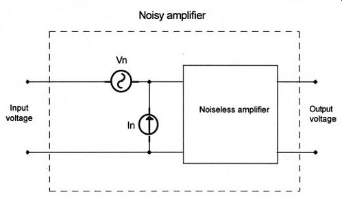
FIGURE 1: Noise sources in an amplifier.
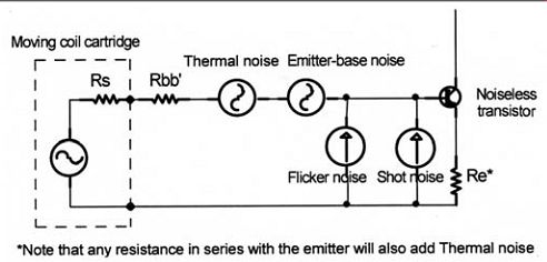
FIGURE 2: Noise sources in real amplifier.
OPTIMIZING TRANSISTOR OPERATING CONDITIONS FOR MINIMUM NOISE
The noise currents Is
and If
increase with increasing Ic , while the voltages Eeb and, to some degree Et (through the rbb' dependence), decrease with increasing Ic so there will be some optimum value of Ic that gives the overall minimum noise contribution. This is given approximately by:
Ic
(opt) = v(hFE)/40 (Rs + rbb' + Re).
For example, with a 2N 4403 (rbb' = 40-O and hFE = 140, see Table 1), a source resistance of 3-O and Re = 10-O, the optimum low noise collector current is
Ic
(opt) = 11.8/2120 = 5.6mA
For a 2SC1316, rbb' = 2O, hFE = 500 (Table 1) so the optimum collector current goes up to around 35mA. However, the dip in noise with collector current is quite broad so the actual choice of current is not particularly critical from the noise aspect (though it is more critical with regard to distortion).
The minimum noise factor at the optimum collector current is given by F = 1 + (rbb' + Re)/Rs + ((Rs + rbb' +Re)/2Rs + Rs/(2(Rs + rbb' + Re)))/(hFE)
0.5 If rbb' + Re roughly equals Rs, and hFE is around 100, the resultant noise factor would be F = 2.1 (NF = 3.2dB).
However, for the same 2N 4403 example (Rs = 3-O, Re = 10-O, rbb' = 40-O) F = 17.1 and NF = 12.3dB, more than 9dB worse than the design ideal. This is because rbb' + Re is significantly larger than Rs. Indeed, the corresponding thermal noise (or "equivalent input noise") from rbb' and Re alone is 116nV or -136.2dBu, compared to the much lower -146dBu from the source itself.
----------------
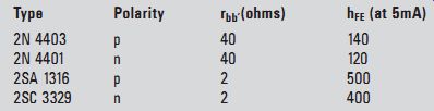
TABLE 1: PARAMETERS FOR SOME CURRENTLY AVAILABLE LOW RBB' TRANSISTORS.
-----------------
You can improve this performance by reducing Re, using a transistor with lower rbb' , and/or using a number of transistors in parallel 10,11 to reduce the effective rbb'. For example, using two 2N4403 transistor stages in parallel effectively halves rbb'
and Re, thereby reducing NF to 8.5dB. However, using a transistor with a lower rbb' = 2-O, such as the excellent 2SA 1316 (Table 1), gives a much better improvement with F = 4.1, NF = 6.1dB, limited now by the noise contribution from Re. Two such stages in parallel would see this reduced to about 4.7dB, quite close to the design target even without any reduction in Re from the rather high notional value of 10-O.
ICs and TRANSFORMERS
Where Rs < rbb' + Re, an alternative solution is to use a transformer to obtain the lowest possible noise figure 12,13, the required turns ratio for low noise being n = v((rbb' + Re)/Rs). Taking again as an example a single 2N4403, with a typical 470R emitter resistor (now as the RIAA input stage), rbb' + Re = 500-O and so, to be properly matched into a 3-O cartridge, n = 13. This low ratio would avoid all of the problems associated with the manufacture of transformers with higher step-up ratios usually required for matching into the high impedance valve input stages.
Another way of looking at the action of the transformer from the noise perspective is to consider that it has effectively reduced Re + rbb' by n2. Proper loading of the cartridge and voltage gain would, of course, also still need to be considered.
Such low impedance and low ratio transformers (n<20) can be made to be nearly perfect with a flat response up to 500kHz and are not particularly expensive to manufacture, though they might be fairly expensive to purchase! Low-noise ICs cannot match the best discrete input stages for the low source resistances under consideration here, as shown in Table 2. With source impedances of around 1k-O, however (e.g., MM cartridges), they are quite competitive (e.g., -121.8dBu with a 5532 and Shure M75ED5).
CONFIGURATION
The noise figure of an amplifier is independent of the input transistor configuration whether common emitter or common base14. This is because the base resistance, which usually limits noise performance, remains in series with the base-emitter junction and signal source whatever the arrangement.
Also, the noise is generally not influenced by negative feedback because signal and noise are both reduced by the same factor (provided that the noise bandwidth remains unchanged). The exception is when the feedback circuitry introduces new impedances which are effectively in series or parallel with the source impedance. To minimize their effects, series resistances must be kept small and shunt resistances high compared to Rs6.
Just about every conceivable configuration for the first stages of MC head amps has been proposed, including BJTs, FETs, and valves. FETs (which tend to have higher corner frequencies) and valves (which require high ratio step-up transformers)
do not generally deliver optimum noise, distortion, and bandwidth performance for the very low source impedances being considered here. You can use BJTs in either common-emitter or common base configurations. For a discussion of the various common-emitter head amp configurations, see Self 15.
A particular advantage of the simple common-base amplifier shown in Fig. 3 is that the gain is essentially R1/R2, which decreases as the source impedance goes up. Because the outputs of MC cartridges also generally go up with impedance, this removes the need for provision to vary gain to any great degree.
Another characteristic of the simple grounded base amplifier is its low input impedance (roughly hFE/40 Ic ). Because there must not be any DC flowing into the cartridge, this would normally necessitate a large value input coupling capacitor. However, capacitors in the input line exacerbate low-frequency noise unless the RC cutoff frequency is very low. This is due to their effect in shunting the 1/f (flicker) and shot noise currents as I mentioned, so their capacitive reactance must be kept small compared to rbb' + Rs + Re. In general, 2p f C = 1/(rbb' + Rs + Re) at 30Hz is a reasonable design target. (For this reason it is better to place any low frequency rolloff components after the low-noise amplifier stage.) One way to avoid this problem is through a current mirror which provides a temperature-compensated offset (adjusted by R2) to bring the emitter voltage to 0V, as in the Hiraga arrangement 16 shown in Fig. 4. However, the distortion of such an arrangement is far from ideal.
-------------------
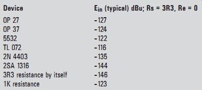
TABLE 2: EQUIVALENT INPUT NOISE VOLTAGES FOR A VARIETY OF DEVICES.
----------
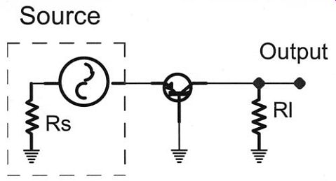
FIGURE 3: AC equivalent circuit for a common-base amplifier.
FIGURE 4: Common-base head amp of Hiraga.
--------------
A more elegant approach is to use complementary transistors in a symmetrical arrangement with their emitters at 0V. This arrangement has the additional advantage that the two rbb' are effectively in parallel, reducing their contribution to the noise. Furthermore, asymmetrical distortions tend to cancel. This was essentially the approach of Leach17 shown in Fig. 5.
You could, of course, add more transistors in parallel 10,18, gaining nearly 3dB in S/N every time the number is doubled until the source impedance becomes the dominating factor. However, the distortion of such an arrangement is still rather high due to the loading effects of R5 (and any additional loading by the input of subsequent stages). This may be alleviated by following the common-base first stage with a common-emitter stage as shown in Fig. 6, thereby increasing the transfer conductance19. A similar arrangement was used in a simple preamp described by Fearby.
Combining complementary units into a symmetrical arrangement then gives the final configuration shown in Fig. 7.
Note that there is no DC path from the battery to earth, so there can be no DC flowing into the cartridge. I used Darlington transistors in the second stage to minimize the loading of the high output impedance common-base first stage. All transistors operate in Class A, so there can be no crossover effects.
It would, of course, be possible to avoid the use of output coupling capacitors by employing additional active devices. However, given the minuscule distortion measured with the current arrangement, I did not think such an extension was justified.
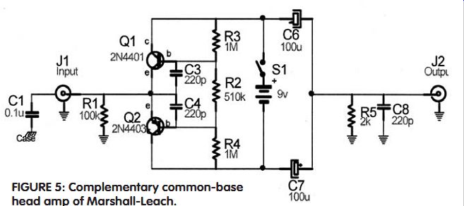
FIGURE 5: Complementary common-base head amp of Marshall-Leach.
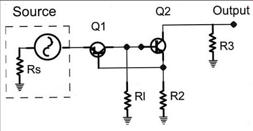
FIGURE 6: AC equivalent circuit for high transfer conductance common-base
stage.
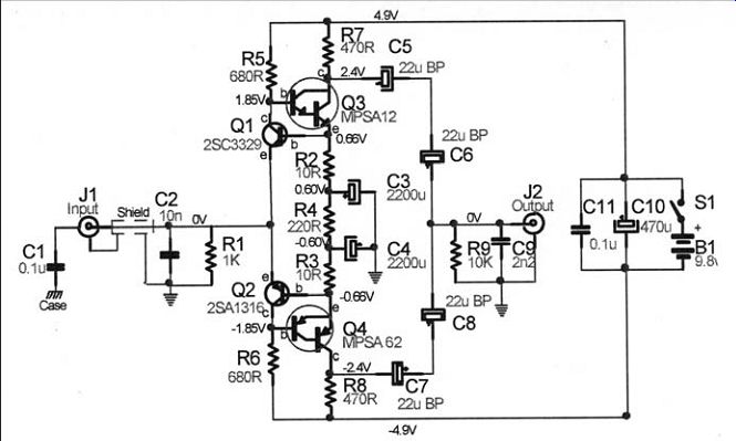
FIGURE 7: Final complementary common-base head amplifier configuration.
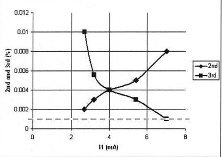
FIGURE 8: Second and third harmonic distortion components as a function of
current through Q1, Q2 (the dotted line represents the noise floor of the measuring
system).
FIGURE 9: THD for the different configurations as a function of output level
(assuming a 3OOsource). The measured data for the head amp are shown as .
DESIGN NOTES AND MEASURED PERFORMANCE
Noise and distortion. As I said, the optimum collector current to minimize noise in the first stage is around 5mA for 2N4401/3 or somewhat higher for a 2SC1316. This is essentially set by R5/6, because the base of the common-emitter stage (and hence the collector of the first transistor) is set at ±3 base-emitter voltage drops (one for the input transistor and two for the common-emitter stage) above 0V. The operating condition for the Darlingtons is a compromise between the required overall gain, set largely by R7/R2, R8/R3, the (low) impedance required for the feedback resistances R2/3 to minimize noise, and consequently the drive requirements of the stage and subsequent distortion produced. The current through the first stage I(Q1/2) also influences the input impedance as it does the distortion performance, as shown in Fig. 8, where I(Q3/4) has been set at 5.5mA.
Note that the distortion figures are quoted for 10kHz and a high 300mV RMS output (remember that the head amp output will be fed into a normal MM input stage which is designed to accept maximum levels below around 30mV). This was necessitated by the exceedingly low levels of distortion produced by the head amp and the noise floor for the measuring system which sets a lower measurable distortion limit of 0.001%. All distortion products vanished into the noise at outputs below 100mV RMS.
In order to explore the distortion performance further, I evaluated the distortion and noise of the different arrangements using a Spice simulation program (Micro-Cap 8.0) and showed them for various levels of output voltage in Fig. 9. The simulation results for the THD of the head amp were slightly above those measured, probably due to inadequate modeling of the Darlington BJTs.
To correct this, I displaced the simulation curve downwards so that it passes through the two measured values.
The simulation also showed that distortion products above the third are virtually non-existent. This was also true for the Leach and Hiraga arrangements.
Of note is the reduction in THD by a factor of nearly 50 in going from the single-ended Hiraga arrangement to the symmetrical Leach arrangement and a similar factor again in going to the present configuration (i.e., the distortion of the head amp presented here is about 67dB below that of the Hiraga!).
Given that the maximum recorded level is around 30m/s corresponding to a MM cartridge output of 30mV, the distortion levels of the head amp at similar output levels (or 600µV input) are below 0.0002% and almost certainly below that of any other part of the reproducing chain. (For comparison, the M-L de sign delivers THD below 0.01% and the Hiraga only below 0.4%, although the distortion is almost entirely 2nd harmonic and therefore probably not quite so objectionable.) The simulation also showed that the level of distortion was not dependent upon which of the transistor pairs shown in Table 1 were used in the input stage. This is, of course, not the case for the noise performance, which is determined by the characteristics of the first transistors.
Measurement of the broadband noise performance is not a simple matter, being only a few microvolts at the output and influenced by any hum pickup resulting from proximity to AC sources (such as transformers, motors, and so on). It is unlikely to differ significantly from the calculated performance as I've mentioned (i.e., NF about 3dB, Ein about -140dBu), so I chose instead to measure the S/N in relation to the real vinyl source.
In relation to actual recorded levels, after RIAA equalization, the head amplifier with 2N4401/3 transistors produced 65.4dB S/N in relation to 3.9cm/ sec at 1kHz from the W&G Professional Test Record (WG25/2434), corresponding to a signal input of 66µV from the FR1 MkIII cartridge. Even with these higher noise transistors, the head amp noise was still about 10dB below the residual surface noise of the record (measured from 300Hz upward to eliminate any rumble content from the result). With the 2SC1316/2SC3329 pair this improved to 70.8dB, indicating that the head amp NF was less than 5dB. The S/N was, in fact, a few dB better than a Shure V15-III cartridge connected to the MM input of the same RIAA preamp that I used with the head amp for the test (probably indicating that there is room for improvement in the noise performance of my RIAA stage).
As I said, you could further reduce the Ein by lowering the value of R2, R3 to, say, 4R7. For 2SC3329/2SA1316 transistors this would reduce Ein from 0.37nV per __/Hertz to 0.31nV per __/Hertz, an improvement of 1.5dB, and would give a NF of 3.2dB. In order to maintain the gain, you would also need to halve R7 and R8 to 220-O and R4 to 110-O to maintain the operating points of the collectors of Q3/4 at around 2.5V to maximize the dynamic range. Reducing R2/3 further to 3R3 (with subsequent changes to R4, R7, and R8) only produces a further 0.3dB noise improvement.
However, the lower impedances presented to Q3/4 then lead to an increased distortion, roughly doubling it for the 3R3 case compared to the 10R chosen. The values chosen represent a good balance between low noise and mini mal distortion. However, if you consider minimum noise important, then you could implement these changes.
Input and Output Impedance. As noted, the input impedance of a common-base amplifier depends inversely upon the collector current, which, in this design, is determined by R5/R6.
With the preferred (i.e., minimum distortion) value of 680-O, the input impedance is about 8-O, and my FR1 MkIII is perfectly happy with this value. If, however, I thought it was desirable to raise this above the "greater than 10-O" recommended by Ortofon, for example, R5/R6 should be increased to 2k2. This will result in a slightly higher distortion level, though at 0.0002% at 10mV peak output it will still remain well below the threshold of the rest of the system.
Increasing R5/R6 to 4k will further raise the input impedance to 20-O, though the THD will then increase to around 0.0006% at 10mV and the noise will similarly increase by a dB or so because of the lower collector current. However, these are still excellent results. The output impedance with the nominated component values is 375O and will remain below 1k for any of the modified values suggested.
Gain. The gain with zero source resistance is 66 (36dB). As the source resistance increases, there will be some attenuation of the input signal by the low input impedance. For a 3-O cartridge, the effective gain is about 50 (34dB).
Bandwidth. Without C5, the 3dB bandwidth of the amplifier is from 4Hz to over 5MHz! However, RF interference is not usually a problem due to the very low input impedance. Furthermore, most well-designed RIAA preamplifiers incorporate some form of low-pass filtering in the input stage. Nevertheless, using 0.0027µF for C5 introduces a rolloff at 150kHz with no measurable degradation of distortion if some margin of safety is required.
Dynamic Range. As noted, the levels of distortion are very small up to outputs of around 300mV RMS, THD rising to 0.06% at 800mV RMS (2V p-p) and rising fairly rapidly thereafter. However, this represents a huge dynamic range, representing 44dB headroom above the reference level of 5mV at 5cm/sec for a MM cartridge. This is a safety margin of nearly 30dB beyond even the hottest recorded levels (30cm/ sec, 15.5dB above 5cm/sec). For my particular FR1 MkIII cartridge, this actually translates to 47dB above 5cm/sec!
FIGURE 10: Suggested PCB layout for one channel.
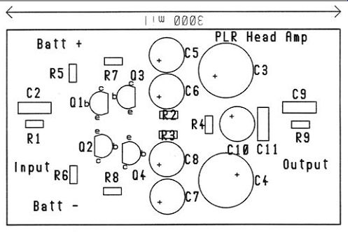
FIGURE 11: Component location.
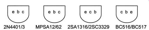
FIGURE 12: Pinouts for the various transistors.
CONSTRUCTION
The recommended PCB layout for a single channel is shown in Fig. 10 and the component locations in Fig. 11. You can build it either as two separate "monoblock" units or with two side-by-side on a single board. Photo 1 shows a board fully populated. The transistor outlines given on the silk-screen overlay are correct for 2N4401/3 and MPSA12/65 transistors.
The 2SA1316/2SC3329 and BC516/BC517 have different TO-92 pinouts as shown in Fig. 12, so you will need to orient them differently to ensure that their base, emitter, and collector leads are properly located.
Note that the pinouts of the transistors should not be checked in the usual way with an ohmmeter because reverse-biasing of the junction can lead to an increase in flicker noise11. The completed prototype is shown in Photo 2.
Metal film resistors are recommended throughout and bipolar capacitors should be used for C5-C7 to minimize distortion22, 23, although you could also use 22µ polar electrolytics back-to-back.
C3 and C4 are normal polar electrolytics, which you should, of course, install with the right polarity. Polypropylene caps are preferred for C2 and C9, while disc ceramics suffice for C1 and C11.
For the emitter common-emitter stages I used MPSA12/62 Darlington transistors. Some suitable alternatives are shown in the parts list. Given the vanishingly small levels of distortion, single BJTs such as BC549/BC559 would probably also be quite satisfactory in these locations. Ideally the 2SA1316/2SC3329 pairs should have their current gains matched to about 10% or better to ensure correct balance.
You should mount the PCB in a steel box to provide some shielding from RF and magnetic hum fields (though I housed the prototype in a die-cast box with satisfactory results). The input and output phono sockets (if used) must have their grounds isolated from the case. Sockets with isolated grounds are readily available, although direct wiring is always an option.
You should mount the circuit board on metal standoffs, with metal star washers placed between the standoffs and the case and the board to ensure good electrical connection. Install capacitor C1 right at the input socket and keep the leads as short as possible to minimize RF interference. Mount the unit away from any transformers or motors to minimize hum pickup. (If you mount the batteries in a separate box, you should shield the power leads, again to minimize any interference.) Because the current draw is around 10mA for each channel, the 9.6V batteries (one for each channel) need to have a capacity of at least 600mAh. I arranged the on-off switch so that when it was in the "off " position, the batteries (each 8 × 600 AA mAh NiCads) are connected to a 15V supply, from the preamp, via two 500-O resistors (one for each battery) to give a 10mA trickle charge when using the system with CD or radio. When in the "on" position, the batteries must be completely isolated (both the positive and negative terminals) from the external supply, requiring a 4-pole, double-throw switch.
Of course, you could remove the batteries or cells from the head amp and charge them at higher rates using a dedicated external charger. In such a case, 2000mAh NiMH cells would give around 160 hours of operation between charges. When not in use, don't forget to switch it off to preserve the batteries.
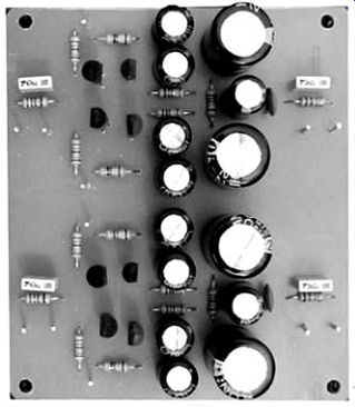
PHOTO 1: The prototype head amp (two channels side-by-side).
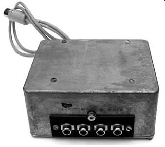
PHOTO 2: Head amp in 4” × 3” diecast box (the gray wires are the twin shielded
power leads that connect with the batteries that were housed in a separate
box in the prototype).
---------PARTS LIST-----
(per channel, double for a stereo pair)
SEMICONDUCTORS
Q1 ..............................2SA1316*
Q2 .............................2SC3329*
Q3 ..............................MPSA12
Q4 ..............................MPSA62
*preferably with current gains matched to about 10%
Alternatives
Q1/Q2: 2SD786/2SB737 (2N4401/2N4403 can also be used but will give 5.5dB higher noise)
Q3/Q4: MPSA 14/MPSA 64 or BC516/BC517 (You could also use normal BJTs such as BC549/BC559 with little increase in distortion. Note that this substitution will change some of the DC voltage levels somewhat.)
CAPACITORS
C1, C11 ....................100n 50V disc ceramic
C2 .............................10n 63V miniature polypropylene
(Wima, 5mm lead spacing)
C3, C4 ....................2200µF 25VW electrolytic
(radial leads)
C5, C6, C7, C8 ........22µF 50VW bipolar (radial leads
C9 .............................2n2 100V miniature polypropylene
(Wima, 5mm lead spacing)
C10 .........................470µF 16VW electrolytic Alternatives
C2 and C9 could be 100V MKT miniature polyester (63V polyester capacitors will give higher distortion)
C5, C6, C7, C8 could be 22µF/50V electrolytic (connected back-to-back on the PCB)
RESISTORS
(all 0.25W or 0.5/0.6W 1% metal film)
R1 ............................................... 1k
R2, R3 ....................................... 10R
R4 ............................................... 220R
R5, R6 ....................................... 680R
R7, R8 ........................................ 470R
R9 ............................................... 10k
Alternatives:
0.5W carbon film would probably be OK.
R5, R6 could be increased to 2k-O for 10-O input impedance, or 3k9 for 20-O input impedance.
SUNDRY OTHER ITEMS FOR THE HEAD AMP:
PCBs (either two single channel or one double channel)
Metal box (preferably steel)
4 × insulated RCA sockets
12 × PCB pins
Shielded and twin shielded wire
Battery clips (2 × 8 cell)
4-pole 2-throw toggle switch if batteries are to be trickle-charged off an external supply; Otherwise, DPDT ½” metal circuit board standoffs Screws, star washers, and so on
-------------
TESTING
Some of the key voltages are shown on the circuit diagram. Check these before connecting the unit to the amplifier, and do not connect the head amp to the MC cartridge before verifying that the input terminals are sitting at 0V. An error here could result in a very expensive blown cartridge. Voltages much different from these (more than a few 10s of mV) indicate a wiring fault or bad component (though they depend to some degree on the actual battery voltage).
When connected to the amplifier, the head amp should be switched on before you select the "phono" input on the preamp to avoid the large switch-on transient. You should ground the turn table at either the head amp or preamp, whichever gives the lowest hum level.
REFERENCES
1. Rossiter, P.L., "An Exponential Horn Loudspeaker," Bulletin of the Australian Acoustical Society, vol. 3, No 1, 10-25, 1975.
2. Futrell, R.A., "The LP Terminator," Jan. '03 audioXpress , pp. 8-15.
3. Maxwell, J., "Phono Cartridge Noise," Audio, 40-41, March 1977.
4. van den Gevel, Marcel, "Noise and Moving Magnet Cartridges," Electronics World, 38-43, October 2003.
5. Self, D., "Precision Preamplifier '96," Electronics World, 540-546, July/Aug. 1996.
6. Walker, H.P., "Low Noise Audio Amplifiers," Wireless World, 233-237, May 1972.
7. Baxandall, P.J., "Noise in Transistor Circuits," Wireless World, Vol. 74 388-92 & 454-9, 1968.
8. van der Zeil, A., "Noise in Solid-State Devices and Lasers," Proc IEEE, vol. 58, Aug. 1970.
9. Foord, A., "Introduction to Low-Noise Amplifier Design," Wireless World, 71-73, April 1981.
10. Faulkner, E.A., "Design of Low noise Audio-frequency Amplifiers," Radio and Electronic Engineer, 17-30, Vol. 36, 1968.
11. Grocock, J.A., "Low-Noise Wideband Amplifier," Wireless World, 117-118, March 1975.
12. Adam, W., "Designing Low Noise Audio Amplifiers," Electronics and Wireless World, 628-633, June 1989.
13. Millett, P., "Moving-Coil Phono Cartridge Transformers," May '02 audioXpress , pp. 58-62.
14. Grey, P.R. and Meyer, R.G., Analysis and Design of Analog Integrated Circuits, Circuit boards are available through Old Colony Sound Lab, PO Box 876, Peterborough, NH 03458, 603-924-9464, Fax 603-924-9467, e-mail custserv @ audioXpress .com www.audioXpress .com Wiley, NY, 1977.
15. Self, D., "Design of Moving Coil Head Amplifiers," Electronics and Wireless World, 1206-1209, Dec 1987.
16. Hiraga, J. Originally published in L'Audiophile. See, e.g., www.bonavolta.ch/ hobby/en/audio/prepre.htm.
17. Leach, W. Marshall, "Build a Preamp," Audio, 36-40, Feb. 1978.
18. Bradford, R. Lee, "Low Noise Moving-Coil Preamp," Wireless World 75, July 1981.
19. Ed Cherry, Private Communication: I thank Ed for suggesting this arrangement.
20. Fearby, L.F., "The Fearby Front End," Hi-Fi News and Record Review 105, Dec. 1979.
21. See, e.g., an unpublished suggestion attributed to Hiraga (www.hilberink.nl), though the same circuit has also been published by Rabeyrolles in L'Audiophile (see, e.g., www. bonavolta.ch).
22. Bateman, C., "Capacitor Sound 6," Electronics World, 44-51, Jan. 2003.
23. Self, D., "Capacitor Distortion," Hi Fi News and Record Review Views, 23, Nov. 1985.