In the best ZEN tradition, the author of this article offers a hybrid amp design...
I’ve been a fan of the Zen amplifier designs by Nelson Pass (“What is the sound of one transistor clapping?” The Audio Amateur, 2/94, p. 10). My incarnation of the Pen ultimate Zen revision IV has been a mainstay in my system for over a year. However, I’ve often wondered about the MOSFET’s suitability to deliver both voltage gain and current gain.
MOSFETs excel at passing current (low impedance), but are questionable as a voltage device (high impedance). In comparison, vacuum tubes are great as voltage devices, especially when operated in the triode mode.
This amplifier design strives to assign each component the role it performs best: the MOSFET used in a current stage and vacuum tubes in a voltage stage. The topology of each stage is selected for linearity, inherent local feed back, and minimum noise.
Part 1 discusses the unity-gain, single-ended MOSFET output stage. Part 2 will discuss the valve voltage amplification stage and wrap up the power supplies, printed circuit boards, and construction.
CHARACTERISTICS OF A MOSFET
Using the MOSFET for voltage gain (Fig. 1) produces many problems for the amplifier designer. The input source is subjected to the MOSFET’s gate- to-source capacitance (CGS) and gate- to-drain capacitance (CGD), which can produce a low-pass filter, rolling off high frequencies. This problem is compounded by a phenomenon called Miller Capacitance.
Small input signals at the gate produce large amplified output signals at the drain. This causes an amplified and dynamic voltage differential between the gate and drain. The input signal must charge and discharge CGD over large voltage swings with the music.
Now the input signal must charge CGS + CGD, but CGD must be charged against a much larger voltage swing. Pass addressed this issue by strengthening the input signal through a P-channel current-booster MOSFET in the Pen ultimate Zen. The boosted input signal overwhelms the Miller capacitance.
However, you can eliminate the Miller capacitance by turning the MOSFET upside-down (i.e., using a P-channel device), in a configuration called the source follower or common drain (Fig. 2).
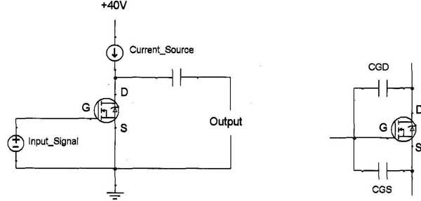
FIGURE 1: Common drain amplifier.
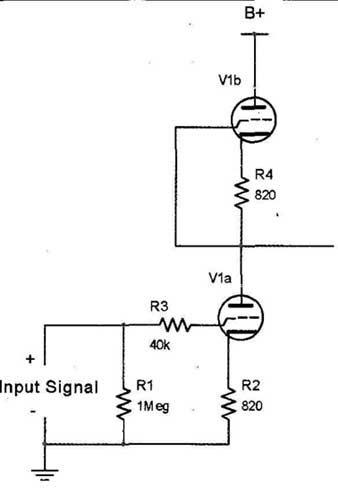
FIGURE 2: Source follower (or common drain).
CONFIGURATIONS
The source-follower configuration is unity gain, having no voltage amplification. The source voltage tracks the gate voltage, so the gate-to-source capacitance (CGS) never sees a voltage differential. Therefore, the only capacitance the input signal must charge is the gate-to-drain capacitance (CGD). This configuration takes a high impedance input signal and converts it to a low impedance output. It employs huge amounts (nearly infinite) of inherent gate-to-source local feedback, very similar to the grid-to-plate feedback of a triode vacuum tube.
As the gate voltage increases (input signal), the source current increases (this current originates from discharging the output capacitor, adding its own current to the already present constant-current source). This causes the source voltage to drop. Because the source current depends on the source voltage, it will be lower than it would have been had the source voltage remained constant. This is what eliminates the capacitance problem, and helps tremendously with linearity.
Now, if you use an N-channel MOS-FET upside-down, all the current will simply flow through the body diode. So you need a P-channel, which can be thought of as an upside-down N-channel but with the body diode pointing in the right direction.
Unfortunately, the selection of appropriate P-channel MOS-FETs is limited, and this won’t make the tube-rollers happy. How about instead of turning the MOS-FET upside-down, the input signal is applied upside-down? (Fig. 3).
Figure 3 looks very similar to Fig. 1, with the exception that the input signal is now applied between the gate and drain. The source should follow the gate signal, but this configuration requires the input signal and MOSFET to share different grounding. One more change, and you’ll have the output stage mastered (Fig. 4).
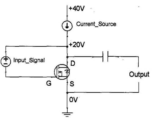
FIGURE 3: N-channel source follower.
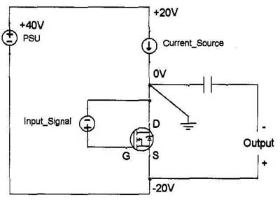
FIGURE 4: N-channel source follower with common ground.
The ground has been moved to the MOSFET’s drain, which allows it to act like a source follower. The power sup ply “floats” with respect to ground, and the amplified signal appears at the negative power supply rail (the MOSFET’s source). I suspect many readers aren’t going to like this unorthodox appearance.
Warning! Because the power supply floats with respect to ground, each channel must have its own independent power supply. This makes dual mono mandatory with this design. Otherwise, the channels will be fighting each other trying to float the power supply differently when music is playing.
With the MOSFET in source-follower configuration, the input capacitance becomes much less worrisome, opening up whole new worlds of component selection. I am currently using the IRFP044 (the favorite choice for the Pass Zen), but I have also tried the IFRP2907Z and incredible monster transistors such as the IXFK80N20. If it has three pins and is an N-channel, try it. The worst that can happen is it either sounds bad or be comes too hot and burns out sooner than expected (sometimes with a little puff of smoke). The rest of the amp will survive, so keep trying. A monster MOS-FET won’t increase your power output. It just dissipates its heat better to the heatsink, increasing reliability and life.
HOW IT WORKS
The constant-current source (covered in detail next) forces a steady current through the MOSFET. When a positive signal is applied to the gate, the MOSFET increases conductivity. The voltage across the MOSFET collapses. This draws current into the drain from load through the output capacitor. Inversely, when a negative signal is applied to the gate, the MOSFET pinches off some current. The drain voltage at tempts to move further away from the source voltage. This re-routes the current from the constant-current source to the load through the coupling capacitor. The maximum output current of this amplifier is limited by how much current can be re-routed from the constant-current source.
The output capacitor needs to be large enough to pass low frequencies. I chose a Panasonic TSHA (low impedance) 10,000uF bypassed with a Solen 2.4uF polypropylene. Whether bypassing is sonically beneficial is up to fierce debate in some circles. Settle the debate for yourself. If you want the Cadillac version, skip the Panasonic and bypass capacitor and use a single Jensen 4-pole electrolytic.
Using a 50V 2A power supply, this amp will output a maximum of 25W into 8ft. Below 8-ohm the amp will run out of current. Above 8-ohm, the amp will run out of voltage. Maximum peak-to-peak output is about ± 18V. You will need reasonably efficient loudspeakers (90dB / watt or better) to play loudly. This output stage prefers a loudspeaker with a flat impedance curve with no significant capacitive (negative) phase angles that correlate to low impedance dropouts. Loudspeaker matching is important.
The source-follower and constant-current MOSFETs combined will dissipate 50V x 2A = 100W Make sure to heatsink properly. This will be covered later.
Some may worry about having the output capacitor in the signal path. Nothing to be concerned about. Almost all amplifiers have coupling capacitors in the signal path. They are just hidden as the bulk capacitors in the PSU. Look at an amplifier schematic and trace the AC signal path through the amp to the loudspeaker. You’ll find the PSU filter capacitors complete the AC signal loop.
In this design, there are no extra capacitors in the signal path. In this case, it happens to be more obvious.
BIASING THE MOSFET
The source-follower must be biased to drop ½ PSU voltage when at idle (Fig. 5). This is performed by voltage divider R3 and R4. C2 filters and stabilizes the bias voltage. The bias voltage is buffered from the input signal by resistor R2. Resistor R1 is a “gate stopper” resistor for MOSFET Q1 to help prevent parasitic oscillations. In practice, R3 is in series with a potentiometer, so precise adjustments of Q1 are possible. I tried an op amp servo loop here for bias control, but found a potentiometer is simpler and just as effective.
Because I’m going to use vacuum tubes for the input stage, Dl was added to clamp any high voltages and protect the MOSFET’s sensitive gate as a precaution.
THE CURRENT SOURCE
Nelson Pass has beaten the current source to death, so I’m not going to repeat much of his work. For a detailed analysis, read his Zen version 2 article at www.passdiy.com.
Here it is in a nutshell: the diode voltage drop (-0.6v) across signal transistor Q3 causes power MOSFET Q2 to mirror the same voltage across R5. Bias current is provided to Q3 through R7 and R8 (Q3 is a signal transistor and only needs a few milliamps). Capacitor C3 is extra noise filtering for the bias current. R6, R9, and C4 help stability. The current source output is approximately (using Ohm’s law) R5/0.6V. For a 2A current, use 0.3-ohm/0.6V = 2A. Because R5 dissipates some heat (1.2W), I used two resistors in parallel to achieve the correct value.
There’s a dozen different ways to make a current source, from the arcane to the ridiculously simple. Google Gary Pimm’s battery powered CCS (arcane) or Nelson Pass Zen Variations Part 1:
Zen-lightenment (ridiculously simple), where he uses a light bulb for a constant current source. I chose the CCS in Fig. 6 because it could accommodate the Pass Aleph circuit.
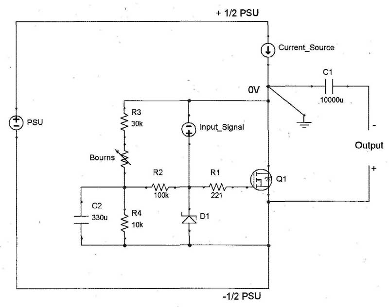
FIGURE 5: Biasing the MOSFET.
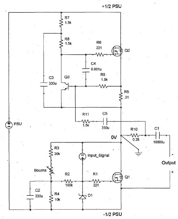
FIGURE 6: Constant-current source.
Components R10, R11, and C5 compose the patented Pass Aleph current source (patent #5,710,522). Pass allows the garage enthusiast (us) to use his patent. Because I built this thing in my garage with no commercial intent, I’m quite appreciative that I can use his contribution to the DIY community.
Here’s a brief explanation of the Aleph: The input signal (music) excites Q1, which causes O1’s source to follow the music. The output signal is routed through R10 and C1. R10 acts as a current shunt and produces a small voltage proportional to the output. This signal is delivered to the base of Q3 through R11 and C5. When Q3 detects output current, it increases the output current of Q2, thereby “boosting” the CCS output a bit. Pass discovered this boost increases power output and decreases distortion.
You can use almost any N-channel MOSFET for Q21 use the IFRP2907Z because of good junction to heatsink thermal coupling. You can even use IGBTs or other types if you get the urge. I have one running with the crazy IXFK80N20, and it works just fine.
Even with the Aleph, the amp acts mostly like a constant-current load on the power supply, so the choke-filtering and capacitance multiplier still work.
THE POWER SUPPLY
To get decent power from this output stage, the MOSFET needs a constant current of about 2A at 50V. The exact current and voltage is not critical, but you need to pay attention to the voltage ratings of your components. I used an Avel-Lindberg 40V + 40V toroidal transformer. I was unhappy with the bbbwwwaaannnggg it made on power up, so I added an Ametherm NTC inrush current protection device. The NTC starts at high impedance, which charges the bulk capacitors slowly, and then drops to very low impedance as it warms up. Be sure to use a dedicated AC fuse to feed the transformer.
With constant-current power supplies, there are some tricks to help reduce noise. I’m a fan of choke-filtered power supplies, so I added a “pi filter” with choke L1. The Jantzen air-core inductors from Parts Express work very well. The 2mH choke has only 0.50-ohm of DC resistance, and is a reasonable selection. The world is your oyster in this department: the Hammond 195T5 weighs i4 lbs and has 100mH. With choke filters, you can use smaller filter capacitors. I used 50,000uF surplus capacitors for the filter capacitors. Values of 10,000uF and up should work well. I didn’t specify these in the parts list. Finding these is up to you.
Following the pi filter is a capacitance multiplier and voltage regulator using an N-channel MOSFET (Q4) and a zener diode (D2) (Fig. 7). I use the IFRP2907Z or a TO-264 pack age darlington (such as the NTE2557). Capacitance multipliers work best with constant-current applications, such as this amp.
The capacitance multiplier is basically a source-follower that tracks a steady and regulated gate signal applied to Q4. Incoming voltage from the PSU rail is filtered and regulated by C6, low pass filter R13 and C7, and zener diode D2. D3 discharges C7 after the amplifier is turned off, otherwise the MOSFET’s VGD would be exceeded. R12 is a “gate stopper” for Q4, to damp the MOS-FET’s gate capacitance and prevent oscillation. Save Ri4 for later. The effectiveness of a capacitance multiplier is determined by the filtering and regulation of the gate signal and the transconductance of Q4.
A side benefit of the capacitance multiplier is the soft-start feature. Because the gate filter circuit R13 and C7 take a few moments to charge, the PSU voltage follows this time constant. This avoids any turn-on thumps or other surges in the amplifier.
Parts selection is not critically important. I use 5mm pin 63V Panasonic FC series for C6 and C7. With a 51V zener, the output of the power supply is about 47V (the MOSFET drops 4V). If you don’t want regulation, just remove the zener entirely. If you value simplicity, skip the entire capacitance multiplier altogether and use a couple stages of passive pi filters.
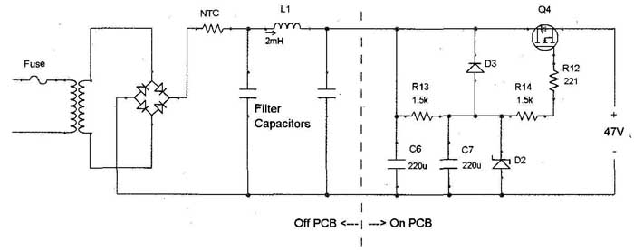
FIGURE 7: Passive and active supply filtering and registration.
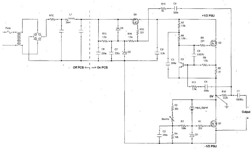
FIGURE 8: Entire output section.
My selection of the IRFP2907Z was based on good thermal junction to heat- sink resistance and high transconductance (for a MOSFET). When making a choice, just make sure Q4’s voltage rating can take the peak no-load voltage of the power supply. Expect this transistor to dissipate about 12-15W (2A x 7V drop is a good estimate, depending on your transformer and zener diode selection). You can use a Darlington transistor for super-high transconductance, which can be several orders of magnitude greater than their MOSFET cousins. I’ve even tried IGBT transistors.
Remember: because the output stage uses a floating power supply, you will need an independent power supply for each channel.
THE WHOLE ENCHILADA
The entire output section is shown in Fig. 8. A few additional parts have been added: Capacitor C9 gives a bit more PSU noise filtering downstream of the regulator. Use a high-quality part. I chose the Solen 2.2uF polypropylene. R15 and C8 give the power supply a boost during large output peaks. When the output current is large, the voltage drop across R10 causes Q4’s voltage to increase a bit. This will force the power supply out of regulation (in the upwards direction), and give the amplifier a couple extra volts during peak output. R14 buffers the zener from the incoming boost signal. Just make sure you don’t violate any voltage ratings of your down stream components.
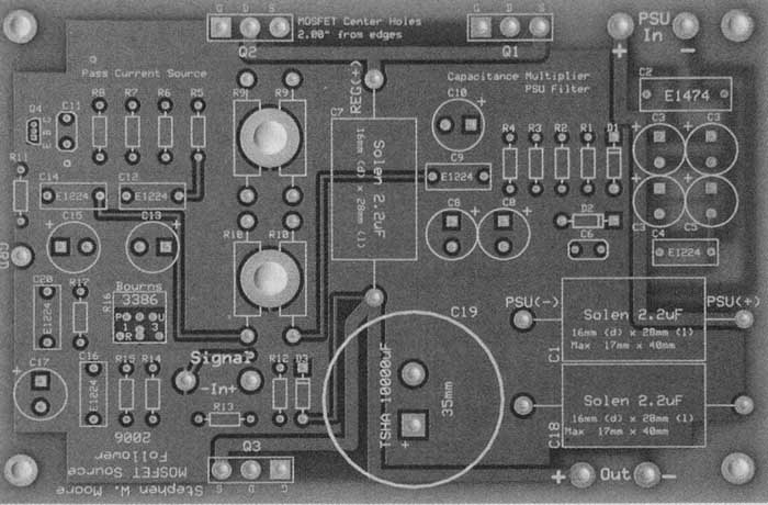
FIGURE 9: PCB.
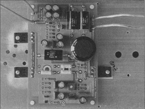
FIGURE 10: Assembled output stage
Figure 9 is a printed circuit board for the output stage and capacitance multiplier. The big circle is for the output capacitor C1. Being the first revision of this amplifier, not all of the component designations on the PCB match the text of this article. Follow good PCB lay out techniques to minimize noise and parasitic oscillations. Figure 10 is a fully functional output stage on an appropriate heatsink.
I wanted the heatsink to have a maximum of 20 degree C rise over ambient when loaded with 120W, so it needed to be rated at 0.18° C/W. This kept the amplifier within reasonable temperatures. The capacitance multiplier was putting out about 14W (7V x 2A) and the amplifier was at 94W (47V x 2A), for a total of 108W. I used 10” of Aavid 65535 for each channel.
The IRPF044N has a junction-to-case thermal resistance (R_jc) of 1.3° C/W plus the case-to-sink resistance (R_cs) of 0.24° C/W for a total of 1.54° C/W. Q1 and Q2 will each dissipate 47W at idle (total of 94W). The IRFPO44N is rated for a maximum power dissipation of 120W, so this seems to be within specification. The junction (inside of the transistor body) will be 1.54° C/W x 47W = 72.4° C over its ambient temperature (the heatsink). If the room is 25° C, then the heatsink will be 45° C, and the junction temperature will be 117.4° C. This is within the junction’s maximum of 175° C. The datasheet specifies a derating of 0.77W/°C when the junction is over 25° C, so the maximum power spec at 117.4° C is 48.8W. When derating is taken into ac count, this transistor is operating (47W at idle) at the very hair’s breadth of the derated specification (48.8W). Perfect! However, don’t expect this transistor to last a long time. Have replacements handy, especially if your room is over 25°C or the heatsinks don’t have generous access to ambient air.
In comparison, the IKFP2907Z has R_jc + R_cs of 0.73° C/W, twice the thermal conductivity of the IRFP044N. In addition, its maximum power dissipation is 310W but with a more severe de-rating of 2W/°C. Using an IRFP2907Z for Q2 (dissipating 47W at idle), the junction temperature is 88° C and the derated maximum power is 184W. This is plenty of headroom, and this transistor should last a very long time. You see how this game is played. It’s up to you to determine sonics.
IN PART 2
Well, this design looks a whole lot like a Pass Zen but with the MOSFET’s input signal upside-down. That’s because it is. I properly used the inherent local gate-drain feedback of the MOSFET source follower to reduce effects of gate capacitance and to maximize linearity. But it still needs gain. Can the same tricks of applying a device’s inherent local feed back be applied in a voltage gain stage? Of course. It’s called a triode valve. In Part 2, I’ll add an appropriate gain stage and take a listen.
REFERENCES
Elliott Sound Products, Project 15, “A Simple Capacitance Multiplier Power Supply for Class-A Amplifiers.” sound.westhost.com/project15.htm
Pass DIY, “Zen Variations, Part 3: Active Supply Regulation,” passdiy.com