In Section 2 of this guide, the tuner, video IF amplifier, sound IF amplifier and output, luminance (or video) amplifier, and the sync and AGC circuits were discussed. All of these circuits are similar to circuits having the same functions in a black-and-white set.
The tuner and IF circuits are modified only slightly to increase the response near the upper edge of the video passband. Additional traps are required to prevent interaction between the 4.5-MHz sound carrier and the 3.58-MHz chroma information. The additional traps make it necessary to move the sound takeoff point "forward" and use a separate sound IF detector. Otherwise, the sound system is conventional. The AGC and sync circuits are nearly identical to the ones found in monochrome receivers.
The luminance channel performs the same functions as the monochrome video amplifier and also it has some additional features. It provides for video delay, performs the retrace blanking, incorporates the brightness control, and, of course, it drives three CRT cathodes instead of one. The luminance channel is direct coupled and this can lead to service problems for the unwary technician.
Vertical Deflection Circuit
The circuit most frequently used to generate the vertical deflection current is a modified free-running multivibrator. The modifications are incorporated to change the usual square-wave output into a waveform which produces a sawtooth current through the deflection coil or yoke. Since the impedance of the yoke is inductive, current lags the voltage; and so the multivibrator output waveform rises very steeply, decays steeply to about one-half its maximum, and then decays at an almost linear rate.
The circuit shown in Fig. 1 is from the Zenith 24MC32 chassis.
This circuit is typical of many receivers although several sets examined used the old, familiar twin triode configuration. We also noted that some circuits have the hold control in the cathode circuit instead of the grid circuit of the normally cutoff tube.
Consider the circuit at a time when the vertical sweep is approaching the bottom of the CRT. The grid of V9 is swinging in a positive direction as current flows upward through R97 to charge the right side of C45. The current through V9 and the deflection coils is increasing at a linear rate. V7 is cut off by the negative charge at the top of C46 although this voltage is approaching the level where the tube can go into conduction.
Shortly before V7 would go into conduction spontaneously, the negative, integrated vertical sync pulse is applied to the grid of V9. The following things all happen in a very few microseconds:
1. The current through V9 is diminished.
2. The field around the deflection coils begins to collapse, causing a positive spike to begin forming at the plate of V9.
3. This positive pulse is coupled to the grid of V7 causing it to conduct.
4. The plate of V7 swings in a negative direction and this negative spike is coupled to the grid of V9.
5. V9 is cut off and the plate rises to a peak of several hundred volts as a result of the total collapse of the field around the deflection coils.
6. The collapsing field drives the electron beam to the top of the CRT, ready to begin another downward scan.
7. The positive spike is coupled from the plate of V9 to the grid of V7. This drives V7 into saturation, the grid draws heavy current, and a negative charge collects at the top of C46. When the spike from the plate of V9 is ended, C46 begins discharging through R93 and R4 and this cuts off V7.
8. As soon as V7 returns to cutoff, its plate swings positive. This positive-going pulse partially discharges C45 and allows V9 to resume conduction.
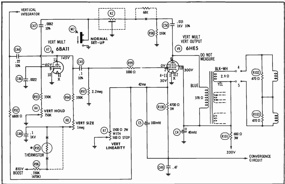
Fig. 1. Vertical multivibrator of the Zenith 24MC32 chassis.
When V9 begins conduction, the trace begins its downward deflection.
The grid voltage of V9 gradually becomes more positive as current flows upward through R97 to charge C45. This increases the current through V9 and the deflection coils to produce the vertical sweep.
There are three controls in the vertical circuit: hold, size, and linearity. The hold control determines the time required for C46 to discharge to the point where V7 can conduct, If this discharge time is too short, (free-running frequency too high) a new vertical scan will have started before the arrival of the next sync pulse and the picture will roll down. If the free-running frequency is slightly lower than the scan rate, the vertical multivibrator synchronizes normally.
The size control determines the plate saturation voltage of V7. The difference between saturation voltage and B + is the amplitude of the signal which is coupled to the grid of V9 and this ultimately determines the amplitude or size of the sweep.
The voltage at the grid of V9 is not completely linear since it is a portion of the exponential charging curve of a capacitor: however, V9 is not linear either (gain is different at various bias levels). By proper adjustment of the linearity control, a level of bias is obtained that causes these two inherent nonlinearities to be equal and opposite.
The network consisting of C47, K2, R98, and C50 shapes the feedback pulse to the grid of V7. The shape of this pulse determines the conduction time of V7 and this determines the retrace time. M7 disables the multivibrator for color setup purposes. R102 and R103 are loading resistors across the deflection coils. They prevent the coils from oscillating at the end of the retrace interval. The resistance of R95 decreases with temperature rise to compensate for the increase in resistance of R96, R8, and R4 as the temperature rises.
Some sets use a vertical centering circuit to control a small DC current which flows through the vertical deflection coils. This current either aids or opposes the vertical deflection current to shift the entire raster up or down.
Horizontal Phase Detector
The horizontal oscillator and its synchronizing circuits used in color sets are no different than those used in b-w receivers. The schematic shown in Fig. 2 is the horizontal phase detector circuit used in the Philco 160T85 chassis. The two inputs to the phase detector are compared to determine their relative timing and a correcting voltage (error signal) is developed to correct the oscillator frequency.
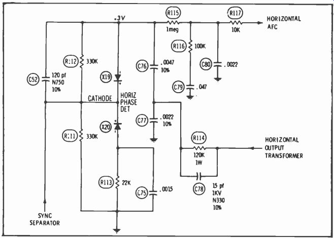
Fig. 2. Horizontal phase detector of the Philco 16QT85 chassis.
Negative sync pulses from the sync separator are applied to the junction of the cathodes of the phase detector diodes and both diodes conduct. This places a negative charge on the tops of C75 and C52. Between sync pulses, these capacitors discharge as follows: C75 discharges downward through RI 13 causing the anode of X20 to be negative with respect to ground.
C52 discharges downward through R 112 causing the bottom of R 112 to be positive with respect to its top.
Since the voltage at the bottom of R 112 cannot be negative with respect to the top of R 113 and the voltage drops across RI12 and R113 are nearly equal, the voltage measured from the top of R 112 (or C52) to ground is nearly zero.
At about the same time that the sync pulse is applied to the junction of the diode cathodes, a negative pulse from the horizontal output transformer is supplied to the junction of C76 and C77. This drives electrons away from the top of C76 and down through R 112 and R 111.
During the interval between pulses, the current flows back up through R 111 and R 112 producing a positive-going sawtooth at the top.
Now consider the interaction of the two separate actions which result from the sync pulse and the feedback pulse. Referring to Fig. 3A, we see the phase relation of the two voltages when the oscillator is operating at the correct frequency.
The sync pulse arrives shortly after the start of the negative-going feedback pulse. Since X19 can conduct only until its anode becomes negative with respect to its cathode, only a portion of the electrons that could be supplied by the sync pulse actually get to the top of C52. During the long interval between sync pulses, some of the electrons required to recharge the top of C76 are supplied from C52 and the remainder Now upwards through R111 and R 112. Since the total-current through R111 and R112 has been diminished by the action of the feedback pulse, the average-voltage at the top of C76 is less positive than it would be in the absence of the sync pulse.
Fig. 3B illustrates the action of the phase detector if the oscillator frequency is too high. The feedback pulse is shifted to the left from its normal position and the anode of X19 is driven farther negative before the sync pulse arrives. As a result, fewer (or none) of the electrons supplied by the sync pulse are actually deposited on the top of C52. During the inter-pulse interval, all of the electrons must flow upwards through R 111 and R112 and the voltage at the top of C76 is more positive.
Inspection of Fig. 3C shows that if the feedback pulse arrives too late (frequency low), a greater portion of the sync pulse electrons reach C52 and the average voltage at the top of C76 is less positive than before.
Referring once again to Fig. 2, R115, R 116, R 117, C79 and C80 form the anti-hunt network. This is essentially an integrating circuit which smooths the voltage at the top of C76 into an almost constant level. If the integrations are too great (time constants too long), horizontal pulling will result because the AFC tube will not correct the frequency quickly enough. On the other hand, too little integration will cause horizontal jitter because the AFC tube will tend to overcorrect the frequency (hunt). From this discussion of the phase detector circuit, we learn that an increase in oscillator frequency results in a positive-going error signal at the grid of V7. While this is true of this specific circuit, some circuits are designed so that the exact opposite is true. That is, increased frequency produces a negative-going error signal in some receivers even though the circuit configuration is quite similar.
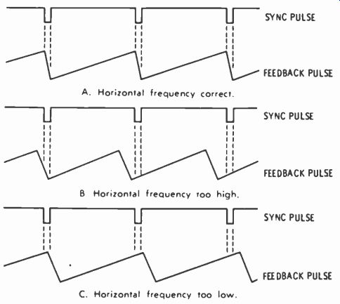
Fig. 3. Horizontal sync and feedback pulses.
Horizontal AFC and Oscillator
Referring to Fig. 4 which is the schematic of the AFC and oscillator circuits of the same Philco I6QT85 chassis, the error signal is applied to pin 9 of V7. However, before attempting to understand the operation of the AFC tube, the operation of the oscillator must be thoroughly understood.
The oscillator is basically a Hartley type although the tank circuit capacity, as well as the inductance, is tapped. The waveshape of the oscillator output is modified by R 124 and C88 before it is applied to the output tube. V7B is grid-leak biased by R122 and C84.
The frequency-determining circuits of the oscillator are L37, C85, C86, and the AFC tube. Insofar as an AC signal is concerned, the AFC tube is shunted across CR6, and so the current through V7A is part of the total current of the tank circuit.
V7A has two inputs, the error signal from the phase detector and also the 15,750-Hz signal present at the cathode of V7B. This second signal is shifted in phase by the combination of C81, R 117, and C80 so that the voltage at the grid of V7A is leading the voltage at the cathode of V713. This leading voltage causes a leading current to flow through V7A and through the tank circuit. From basic electronic theory, we recall that a leading current is a capacitive current, and so the current of V7A appears as an additional capacitive current in the tank. Thus, as the error signal goes positive, the capacitive current increases and the resonant frequency decreases to reduce the error.
R4 and R 120 set the bias of V7A and determine the free-running frequency of the oscillator. The error signal at the grid of V7A causes the capacitive current to vary above or below this level to maintain horizontal sync.
It was pointed out earlier that the direction of the error signal generated by the phase detector can be either positive or negative for a given frequency error. It is also possible to change the AFC circuit from the one shown in Fig. 4 so that a positive error signal at the grid will increase the frequency rather than decrease it. One way of doing this is to interchange the values of C80 and C8I. Now, the feedback would lag and the current through V7A would appear inductive rather than capacitive.
There are numerous other circuits which are used to generate the horizontal time base. Space limitations do not allow an exhaustive analysis of each of them in this course. For most service problems, the technician will be able to solve the difficulties if be will simply take time to identify the frequency determining components and determine the direction of the error signal from the phase detector.
Horizontal Output and High-Voltage Circuits
Regardless of the oscillator and AFC circuits used, the designs of the horizontal-output sections used by various manufacturers are similar.
In many respects, the circuits are the same as ones used in monochrome receivers, but the whole horizontal deflection system has been "beefed up" for several reasons:
1. The ultor (high-voltage anode) voltage (about 25 kv) is higher than it usually is in b-w receivers, and the CRT beam current is increased three-fold.
2. The shunt regulator draws additional current from the ultor supply.
3. The boosted B + has a higher potential and the load is greater.
4. The focus rectifier and bleeder, the convergence circuits, and the pincushion circuits extract power from the horizontal output circuit.
The schematic of the horizontal output and high-voltage circuit used in the Zenith 25LC30 chassis is shown in Fig. 5. The yoke is driven in the conventional manner by taps on the primary of the high-voltage transformer. A secondary winding is used to obtain the voltages necessary for convergence, horizontal AFC, and keying of the AGC, color killer, and burst amplifier.
The anode supply for the focus rectifier is obtained from a tap on the primary of the high-voltage transformer. The output of V I S is divided by the bleeder consisting of R 130. R 13 I . 12 132. and R20; and the focus voltage is controlled by the setting of R20. C68 is a filter for the focus supply and R133 is an arc protector.
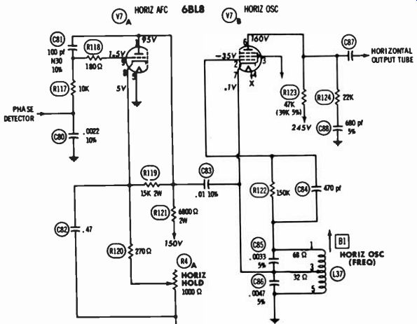
Fig. 4. Horizontal oscillator and AFC of the Philco 160T85 chassis.
The ultor voltage is developed in the usual manner but, unlike b-w supplies, it is regulated by a shunt regulator. Regulation is accomplished by the special regulator tube (V 16). R I9 is used to set the bias on V 16 so that it is near cutoff when an all-white picture is being displayed. As portions of the picture are made black or gray, the CRT beam currents decrease and the ultor supply voltage tends to rise. The boosted B + also rises and this positive-going voltage is used to decrease the bias on V16. Thus, V16 conducts more, the load on the ultor supply remains constant, and the ultor voltage is stabilized.
Some manufacturers use the average potential of the CRT cathodes as a control voltage for the ultor regulator. A black picture is produced by a positive-going voltage at the CRT cathodes, and this voltage (in lieu of the boosted B +) is used to increase the conduction of the regulator tube.
A rather unique approach to the problem of high-voltage regulation is illustrated in Fig. 6. This is a schematic of the horizontal output and high-voltage section of the Admiral 1G1155-1 chassis. Notice that no shunt regulator is used.
A feedback pulse from the secondary winding ( terminals 1 and 2) of T4 is rectified by X10 and the resulting voltage is added to the bias supply for the horizontal output tubes. This total bias determines the amount of drive to the high-voltage transformer and, finally, the potential of the ultor supply.
As the CRT beam currents increase and load the supply, the amplitude of the feedback pulse is decreased and this results in a lesser bias voltage at the grids of V 10 and V11. This causes V 10 and V11 to conduct more heavily to increase the ultor voltage.
While this system is adequate, it does allow some variations in the high voltage. In order to maintain good focus over a range of ultor voltages. the focus voltage is made to "track the ultor voltage. This is accomplished by. R 141 and R 142 along with their filter. C99. As the CRT beam currents increase, the voltage across R141 and R142 increases and this voltage is added to the output of the focus rectifier to adjust the focus automatically for changes in CR"T current. A slight change in width as the brightness control is rotated is normal in receivers using this circuit.
The horizontal output and high voltage circuits of the RCA CTCI6 chassis are shown in Fig. 7. In this circuit, the focus rectifier is connected to the plate of the horizontal output tube and develops 4 to 4.5 kv. The ultor-voltage supply and regulator are similar to the Zenith chassis discussed earlier. but the regulator control voltage is derived from the CRT cathodes.
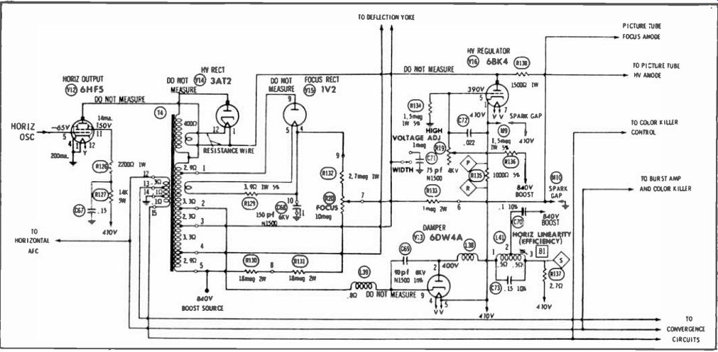
Fig. 5. Horizontal output and high-voltage circuit of the Zenith 25LC30 chassis.
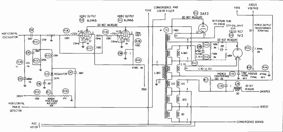
Fig. 6. Horizontal output and high-voltage circuit of the Admiral 1G1155-1
chassis.
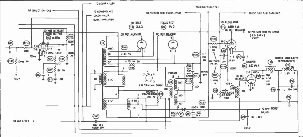
Fig. 7. Horizontal output and high-voltage circuit of the RCA CTC16 chassis.
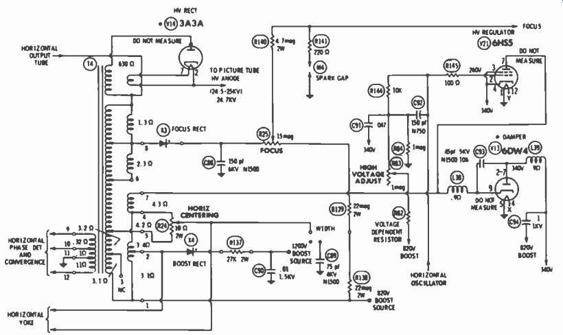
Fig. 8. Horizontal output circuit in Zenith 23XC38 chassis.
The horizontal-centering problem is solved by driving the yoke with two identical windings of the high voltage transformer. A 10-ohm potentiometer used as a centering control is connected between terminals 3 and 4, and a small DC potential exists across it. One end of the yoke is connected to the center arm of the control. Depending on the setting of the control, a small DC current can be caused to flow in the yoke to change the centering.
A third method of high voltage regulation has been developed in the Zenith 23XC38 chassis. The horizontal output circuit is shown in Fig. 8. This circuit uses a type 6HS5 regulator (V21) whose cathode and plate are connected to B + and a tap of the horizontal-output transformer, respectively. Since the tube is operating at potentials which are much lower than those encountered in the conventional shunt regulator circuit, there is no need for radiation shielding or a double ended envelope for the tube.
The control signal for V21 is derived from a divider network consisting of R82, R83, and R84 connected between a portion of the boosted B+ supply and ground.
R83 is used to set the bias level of V21 and this ultimately adjusts the ultor supply voltage. A second voltage is also applied to the grid of V21. This is a positive pulse taken from the cathode circuit of the horizontal oscillator.
Assume a white raster which results in maximum loading of the ultor power supply. The boosted B + potential is minimum and the bias on V21 is maximum. Under these conditions, the conduction of V21 is minimum and the regulator has little effect on the output voltage of the ultor supply.
Under black-raster conditions, there is no load on the ultor supply and this voltage tends to rise. The boosted B + also tends to rise and the bias of V21 is reduced. The horizontal-oscillator pulse causes V21 to conduct during the retrace interval and this conduction loads the horizontal output transformer.
Stated another way, V21 clips the positive excursion of the "ringing" or flyback pulse of the horizontal output transformer and this tends to reduce the ultor supply voltage.
The amount of clipping (or loading) is determined by the boosted B+ potential which, in turn. is determined by the load on the ultor supply. As the raster changes from black to white, the conduction of V21 becomes progressively less and so the ultor supply voltage is stabilized.
The regulator tube is pulsed on only during horizontal retrace for two reasons:
1. Since V21 is cut off during the forward scan, it does not affect the width of the raster.
2. Since V21 conducts only during retrace, the duty cycle is low and only a minimum amount of power is extracted from the horizontal-output circuit. This also minimizes the plate-dissipation requirements for V21.
Summary
In this Section, we have analyzed the power supply and deflection circuits. The principal difference between these circuits and their b-w counterparts is that greater power handling capability and greater stability are required in the circuits of color receivers.