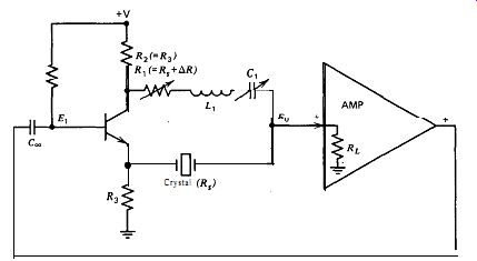
Figure A.1. Simplified RLC half-bridge circuit.
| Home | Audio mag. | Stereo Review mag. | High Fidelity mag. | AE/AA mag. |
1. BACKGROUND
3. FUNDAMENTALS OF CRYSTAL OSCILLATION
4. CIRCUIT DESIGN CHARACTERISTICS
6. SHORT-TERM FREQUENCY STABILITY
7. ANALYSIS OF PHASE VERSUS FREQUENCY
8. TRIMMING THE CRYSTAL FREQUENCY
10. DISCRETE TRANSISTOR OSCILLATORS
11. INTEGRATED CIRCUIT OSCILLATORS
13. OPTIMIZING THE OSCILLATOR CIRCUIT
===== below content is on this TOC page, below =====
References
Bibliography
Appendix A: RLC Half-Bridge Circuit
Appendix B: Emitter Coupled Harmonic Circuit
Appendix C: Feedback Bridge Circuit Index
==========
1. J. M. Miller, Piezo Electric Oscillation Generator. U.S. Patent #1,756,000, April 1930. Both Miller and Pierce circuits.
2. G. W. Pierce, Electrical System. U.S. Patent #1,789,496, January 1931. Both Pierce and Miller circuits.
3. G. W. Pierce, Electrical System. U.S. Patent #2,133,642, October 1938. Both Pierce and Miller circuits.
4. S. Sabaroff, Voltage Stabilized High Frequency Crystal Oscillator Circuit. Proc. IRE 25(5), 623-629 (1937). Quartz crystal version of Colpitts LC oscillator.
5. L. A. Meacham, Bridge-Stabilized Oscillator, Proc. IRE 26(10), 1278-1294 (1938). Resistance bridge circuit.
6. F. Butler, Series Resonant Crystal Oscillators. Wireless Eng. 23(6), 157-160 (1946). VHF harmonic circuits.
7. H. Goldberg and E. Crosby, Jr., Series Mode Crystal Circuits. TELE-TECH, 24-27 and 86 (May 1948). Cathode coupled circuits.
8. W. A. Edson, W. Clary, and J. Hogg, High Frequency Crystal-Controlled Oscillator Circuits. Final Report, Project 131-45, December 1950. Georgia Institute of Technology, State Engineering Experiment Station, Atlanta, Georgia. C.A.D.O. No. EEL-C4971 and T.I. 108261. VHF harmonic circuits.
9. W. A. Edson, Vacuum Tube Oscillators. Wiley, New York, 1953. Classic reference on oscillator circuits.
10. D. Firth, Quartz Crystal Oscillator Circuits Design Handbook, March 1965, ASTIA AD460377. Best reference on Pierce circuit and Butler common base harmonic circuit.
11. A. W. Warner, Design and Performance of Ultraprecise 2.5 mc Quartz Crystal Units. SSTJ 39(5), 1193-1217 (1960).
12.
13.
14.
15.
16.
17.
18.
19.
20.
21.
22.
23.
A. W. Warner, Frequency Aging of High-Frequency Plated Crystal Units. Proc. IRE 43(7), 790-792 (1952).
H. E. Bornmel, W. P. Mason, and A. W. Warner, Experimental Evidence for Dislocations in Crystalline Quartz. Phys. Reu. 99(6), 1894-1896 (1955).
H. E. Bornmel, W. P. Mason, and A. W. Warner, Dislocations, Relaxations, and An-elasticity of Crystal Quartz. Phys. Rev. 102(l), 64-71 (1956).
R. Harrison, Survey of Crystal Oscillators, Hum Radio Magazine, lo-22 (March 1976).
H. Bahadur and R. Parshad, Operation of Quartz Crystals in Their Over tones: New Methods. Indian J. Pure Appl. Phys. 13, 862-865 (1975). Harmonic operation of Colpitts with resistive load on emitter.
E. J. Post and H. F. Pit, Alternate Ways in the Analysis of a Feedback Oscillator and Its Application. Proc. IRE 39(2), 169-174 (1951). Analysis of Meacham circuit.
J. K. Clapp, Bridge-Controlled Oscillator. Gen. Radio Exp. 18(11), l-4 (April 1944); 18(12), 6-8 (May 1944). Meacham circuit without transformers.
S. D. Culp, Crystal Oscillator Uses Logic Gates. EEE, 87 (July 1970). TTL inverter circuit.
B. Blood, Interfacing with MECL 10,000 Integrated Circuits. Motorola Ap plication Note An-720, February 1974.
R. J. Matthys, A High Performance VHF Crystal Oscillator Circuit, RF Design, pp. 31-38, Mar. 1987. Simplified and improved Emitter coupled harmonic circuit.
M. M. Driscoll, Two-Stage Self-Limiting Series Mode Type Quartz Crys tal Oscillator Exhibiting Improved Short-Term Frequency Stability, 1EEE Trans. In.&. 6 Meas., VIM-22, n2, June 1973. Original Emitter coupled harmonic circuit.
A. Benjaminson, Balanced Feedback Oscillators, U.S. Patent #4,661,785. Bridge oscillator circuit.
Anderson, T. C. and G. F. Merrill, Crystal-Controlled Primary Frequency Standards: Latest Advances for Long Term Stability. IRE Trans. Instrum., 136-140 (September 1960).
Buchanan, J. P., Handbook of Piezoelectric Crystals for Radio Equipment De signers, October 1956, ASTIA AD110448. Quartz crystals and oscillator circuits.
Burgoon, R., & R. L. Wilson, Design Aspects of an Oscillator Using the SC Cut Crystal, Proc. 33rd Ann. Symp. on Freq. Control, pp. 411-416, 1979. Oscillator circuit for SC cut crystals.
Felch, E. P. and J. 0. Israel, Simple Circuit for Frequency Standards Employing Overtone Crystals. Proc. IRE 43(5), 596-603 (1955).
Frerking, M., Crystal Oscillator Design and Temperature Compensation, Van Nostrand Reinhold, 1978.
Gerber, E. and R. Sykes, State of the Art-Quartz Crystal Units and Oscillators, Proc. IEEE 54(2), 103-116 (1966).
Gruen, H. E. and A. 0. Plait, A Study of Crystal Oscillator Circuits. Final Report, Armour Research Foundation, August 1957, ASTIA AD149085. Wide variety of circuits.
Hafner, E., Crystal Resonators. ZEEE Trans. Sonics Ultra-sonics SU-H(4), 220 236 (October 1974).
Lane, M., Transistor Crystal Oscillators to Cover Frequency Range 1 kHz-100 MHz, Report No. 6513, September 1970. Australian Post Office Research Laboratories, 59 Little Collins St., Melbourne, Victoria, Australia 3000.
Matthys, R. J., Survey of VHF Crystal Oscillator Circuits, Proceedings of RF Technology Expo, pp. 371-381, Feb. ll-13,1987. RF Design, Englewood, Colo. Comparison of VHF oscillator circuits.
Neubig, B., Design of Crystal Oscillator Circuits, VHF Communications, Part I pp. 174-189, n3, 1979, Part 11 pp. 223-237, n4, 1979. Collection of crystal oscillator circuits.
PaR2en, B., Design of Crystal and Other Harmonic Oscillators, Wiley Interscience, 1983.
PR2edpelski, A. B., VHF and UHF Crystal Oscillators, RF Design, pp. 63-65, July, 1990. Collection of UHF Oscillator circuits.
Pustarfi, H. S., Improved 5 mHz Reference Oscillator for Time and Frequency Standard Applications. IEEE Trans. IM-15(4), 196-200 (December 1966).
Smith, W. L., Miniature Transistorized Crystal-Controlled Precision Oscillators. IRE Trans. Instrum., 141-148 (September 1960).
Smith, W. L., Precision Quartz Crystal Controlled Oscillators Using Transistor Circuits. Bell Labs Record 42(8), 273-279 (1964).
Sykes, R. A., High Frequency Plated Quartz Crystal Units. Proc. IRE 36(l), 194-197 (1948).
Warner, A. W., High Frequency Crystal Units for Primary Frequency Stan dards. Proc. IRE 40(9), 1030-1033 (1952).
Williams, J., Bridge Circuits, Application Note 43, Linear Technology Corp., Milpitas, Calif., July 1990. Crystal oscillators with sine wave outputs of low distortion.
RLC HALF-BRIDGE CIRCUIT
This circuit is a late improvement on the already outstanding modified Meacham, and since it performs equally well, it is included here as an Appendix.
The modified Meacham circuit described in Section 5.11 gives out standing performance, but it is very difficult to design. Its design can be made easier by moving the amplifier's LC network over to the resistive arm of the half-bridge. All the frequency controlling elements are then in the bridge arms, and the amplifier can have a flat frequency response. A wide range of noninverting amplifier designs can be used with this new circuit arrangement.
A simplified schematic of the RLC half-bridge circuit is shown in Fig. A.1. The two bridge arms are driven out-of-phase, with the transistor operating as a split-load phase inverter. The operation of the bridge is described in detail in Sections 5.11 and 7.5, but in essence the out-of phase signal through the resistive bridge arm R, cancels out part of the crystal's internal resistance R,. This effectively increases the crystal's in-circuit Q, which in turn increases the short-term frequency stability.
And the higher the amplifier's gain, the more the crystal's in-circuit Q can be increased.
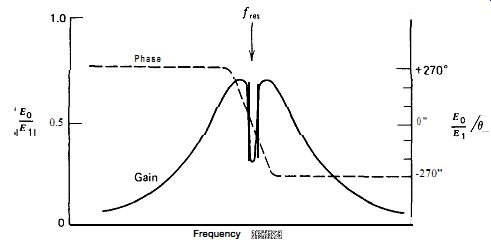
Figure A.2 shows the gain and phase shift characteristics of the half bridge in the RLC half-bridge circuit. L, and C, are series resonant at the crystal's fundamental frequency. The overall broad peak of the gain curve is due to the series resonance of L, and C,, and the sharp "hole" or slot at the peak is due to the crystal's series resonance. The phase shift through the bridge changes from +270 degr. (lead) below the resonant frequency to -270 degr. (lag) above resonance.
The design of the RLC half-bridge circuit is as follows. In Fig. A.1, R, has the smallest possible value that will still let the circuit oscillate, and …
Figure A.1. Simplified RLC half-bridge circuit.
… allow the maximum crystal in-circuit Q to be obtained (the circuit will ot oscillate if R, is less than R,, except spuriously). This requires the highest possible amplifier gain without the amplifier oscillating spuriously. C, is tuned to resonance with L, at the crystal's fundamental fre uency. C, can be varied slightly from its resonance value to trim the crystal's oscillation frequency.
A high L1C1 ratio is desirable. A low L1/C1 ratio gives a broad frequency transmission band to the half-bridge, and the crystal then oscillates at its 3rd or 5th harmonic where the bridge gain is higher, rather than at its fundamental frequency. A high L1/C1 ratio gives a narrow frequency transmission band, so that the bridge gain at the crystal's 3rd and 5th harmonics is too low for oscillation, and the crystal then has to oscillate at its fundamental frequency. The inductance L, should be reason ably large, with its maximum value limited by its internal AC resistance.
The internal AC resistance of L, should be less than the crystal's internal resistance R,, so as not to limit the maximum crystal Q obtainable in the circuit.
The bridge load resistance RL in Fig. A.1 should not have too high a value. RL should be about 2-10 times the crystal's internal series resistance R_L. If R_L is much larger than this, the circuit will not be stable when R, is set less than R, to check the amplifier's stability. And although it is not shown in Fig. A.1, a small capacitance equal to (or slightly greater than) the crystal's external terminal capacitance C,, is tied across the R,L,C, bridge arm to balance out the crystal's terminal shunt capacitance Figure A.3 shows a schematic of the RLC half-bridge at 1 MHz. The amplifier uses two transistors in an emitter coupled configuration, with an emitter follower at the output. Q2 provides a relatively high load resistance to the bridge at point A, so that the bridge load resistance RL is primarily determined by the emitter biasing resistor R2. Two diodes in parallel (III-DZ) with reversed polarity provide an amplitude clamp to drive the crystal with a low-excitation, constant-amplitude signal. The amplifier has a gain of 50 X from point A to point B in Fig. A.3. The bridge operates with a 2 : 1 voltage excitation ratio between the two bridge arms. With a 2: 1 half-bridge, the theoretical minimum value for R1 is RJ2, or 120 a. The effective value of R, has to include the AC resistance of L, (60 0). This gives a ratio of the practical to theoretical minimum values for R1 of (110 + 60)/120 = 1.4, a desirably low ratio (1.0 is the unattainable minimum, corresponding to infinite Q).
The frequency changes 0.0 ppm when the power supply voltage is changed from 4 to 6 V, but this is dependent on the tuning of Cr. The short-term frequency stability measured 0.1 ppm, at the limit of the measuring equipment available. An oddity of the circuit is that C, has to be greater than 17 pF, much more than the required bridge balancing value of 2Co (6 pF), to make the circuit stable and prevent spurious oscillation when RI is set less than the minimum value for fundamental oscillation.
Figure A.4 shows a schematic of the RLC half-bridge at 100 kHz. This circuit is similar to the 1 MHz circuit in Fig. A.3. The frequency changes 0.4 ppm when the power supply voltage is changed from 4 to 6 V, but this is dependent on the tuning of Cr. The short-term frequency stability measured 0.1 ppm, at the limit of the measuring equipment available.
The amplifier gain from point A to point B in Fig. A.4 is 57 X. The theoretical minimum value of R1 in this circuit is R,/2, or 200 0,. This ...
Figure A.3. RLC
half-bridge at 1 MHz.
... gives a ratio of the practical to theoretical minimum values for R1, including the AC resistance of Lr, of (420 + 11)/200 = 2.1. R3C3 prevents parasitic oscillation in the circuit. C, has to be at least 19 pF, slightly greater than the required bridge balancing value of 2C0 (16 pF), to make the circuit stable and prevent spurious oscillation when R, is set less than the minimum value for fundamental oscillation.
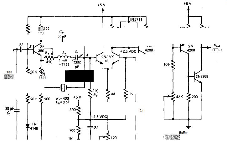
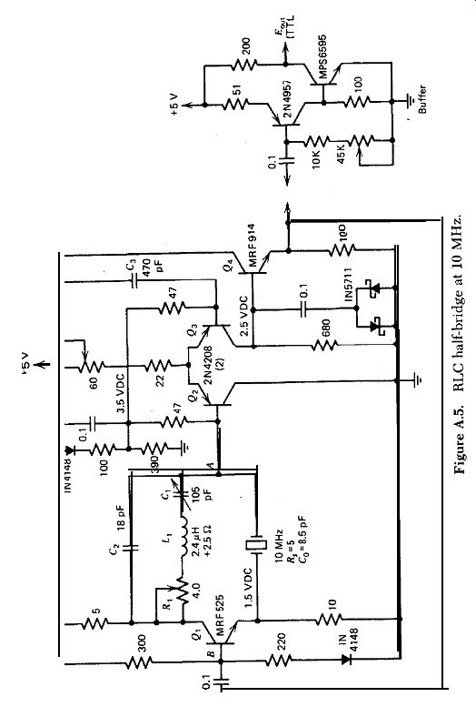
Figure A.4. RLC half-bridge at 100 kHz.
Figure A.5
Figure A.5 shows a schematic of the RLC half-bridge at 10 MHz. The base input resistance of the npn phase inverter Q, is very low and is best driven by an npn type of emitter follower. The emitter coupled amplifier Q2-Q3 uses pnp transistors, so that an npn transistor can be used for the emitter follower Q4. The amplifier gain from point A to point B in Fig. A.5 is only 17x and is limited by the low gain of the high-frequency pnp transistors available and the loss in gain from Cs's phase lead correction.
The amplifier has a phase lag of 29 degr., which is compensated to zero by 29 degr. of phase lead from C,. The frequency changes 1.2 ppm when the power supply voltage is changed from 4 to 6 V. The short-term frequency stability measured 0.1 ppm, at the limit of the measuring equipment avail able. The theoretical minimum value of R, in this circuit is RJ2, or 2.5 R. This gives a ratio of the practical to theoretical minimum values for R,, including the AC resistance of L,, of (4 + 2.5)/2.5 = 2.6. A heat sink is required on Q, in Fig. A.5 The crystal waveforms vary from good to very good in the three circuits. All three circuits are stable and do not oscillate spuriously when the resistance R, is set at 0 a, that is, at less than the minimum value for oscillation, RJ2. The stability margin is somewhat small in the 100-kHz and lo-MHz circuits, but the test shows that the amplifier circuits are stable. In addition, the three circuits are stable and do not oscillate when the crystals are removed from the circuits. No temperature tests have been made on the circuits.
As can be seen from the above data, the RLC half-bridge gives the same outstanding performance as the modified Meacham. It does this with a reasonably simple "flat amplifier" design, compared to the much more difficult tuned amplifier circuit that's used in the modified Meacham. Adding L,C, to the bridge arm makes the half-bridge part of the circuit a little more complex, but the impact is not nearly as great as the elimination of the tuned amplifier. Because it gives the same performance with a simpler circuit, the RLC half-bridge is an improvement on the modified Meacham circuit.
++++++++++++++
EMITTER COUPLED HARMONIC CIRCUIT
Appendix B was originally published in RF Design, Mar. 1987 0. With permission, Cardiff Publishing Co.
The Emitter coupled harmonic circuit has the best short term stability of any harmonic circuit tested by the author to date. Originally described by Driscoll [22], the circuit has been simplified and improved by eliminating a transistor stage and a transformer, and adding an RC phase lag network. The basic schematic of the improved Emitter coupled harmonic circuit is shown in Fig. B.1. It uses only one transistor, and operates at frequencies up to 100 MHz. The oscillator's output is a clean sine wave.
The crystal is connected as the transistor's emitter load impedance, and controls the oscillation frequency by controlling the transistor's gain and phase shift. The circuit's very good short term frequency stability comes from the high capacitance load shunted across the crystal by the transistor's emitter output, which keeps the crystal's in-circuit Q high. The large capacitive loading on the crystal means the resistive loading losses that reduce in-circuit Q will be low. In addition, the crystal has direct emitter control of the transistor's gain. This is almost an optimum crystal oscillator circuit the crystal is located at the lowest power point in the circuit (minimum crystal heating), and the output signal is taken at the highest amplitude point in the circuit (maximum signal/noise ratio and minimum external amplification).
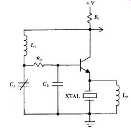
Figure B.1. Basic circuit of Emitter coupled harmonic oscillator.
B.1. HOW IT OPERATES
The basic circuit is shown in Fig. B. 1. It has positive feedback and oscillates at a frequency of 0 degr. (or 360 degr.) phase shift, presuming the loop gain is greater than one. The & Cl network normally operates just above resonance, and provides about 120 degr. of phase lag. The R,C, network provides an additional phase lag of about 60 degr. The transistor provides 180 degr. of phase reversal, giving a total of 0 degr. (or 360 degr.) around the circuit's feedback loop.
The inductor Lz can be any value larger (2X - 20X) than what will resonate with the crystal's terminal-to-terminal capacitance C,. The purpose of Lz in the circuit is not understood, but the circuit will not oscillate if L2 is equal to or less than this resonance value. The circuit also will not oscillate if a resistor is substituted for inductor Lz.
In practice, the crystal's internal impedance, which is lowest at series resonance, controls the transistor gain. It can also vary the normal 180 degr. phase shift through the transistor stage by 250 degr. The crystal uses these gain and phase shift mechanisms to control the oscillation frequency.
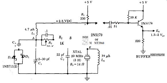
Figure B.2. Emitter coupled harmonic circuit at 20 MHz.
B.2. TYPICAL CIRCUITS
A typical circuit at 20 MHz is shown in Fig. B.2. The crystal, which has an internal series resistance R, of 14 ohms, oscillates at a third harmonic. The diode clamp Di - D, limits the oscillation amplitude, to avoid overdriving the crystal. The transistor operates continuously in a linear mode over a complete cycle of oscillation, and reflects a reasonably constant load across the crystal at all instants of time. Fig. B.3 shows the oscillation waveforms at various points in the circuit. The calculated gain and phase characteristics for the oscillator's entire closed loop in Fig. B.2 are shown in Fig. B.4. Note the steep phase change with frequency, an indication of good frequency stability.
The circuit values in Fig. B.2 are derived as follows. The transistor's gain is proportional to the ratio of the collector's load impedance to the emitter's load impedance. At the crystal's series resonant frequency, the gain is approximated by the ratio R,IR,s, where Ri is the collector's load resistance and R, is the crystal's internal resistance. R, is fixed by the crystal and the operating frequency. R1 is selected as a ratio to R, so as to provide enough gain for the circuit to oscillate. L1 is selected to have a high shunt impedance with respect to R, and still resonate at or just below the oscillation frequency with a reasonable-sized variable capacitor C1. R1 is selected to provide a relatively high load resistance to C1.
The capacitive impedance of C2 is reflected across the crystal by the transistor's emitter, multiplied by the transistor's current gain H,,. To provide a low impedance load and high Q for the crystal, C2 should be as large as possible, consistent with R2C2 providing a large phase lag without too much gain loss. R3 controls the transistor's DC current, which is conveniently adjusted to set the transistor's DC collector voltage at half the power supply voltage. At low frequencies, the 2N5179 transistor in Fig. B.2 is a good selection. At 50 MHz and above, the higher gain of the MMT3960 is needed.
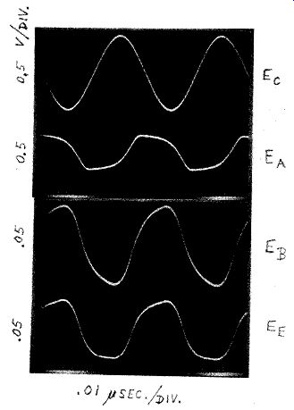
Figure B-3. Waveforms for 20 MHz oscillator circuit in Fig. B.2.
The actual external load network seen by the crystal's resonant elements is shown in Fig. B.Sa. This load network needs to be simplified down to an equivalent series RC network, such as is shown in Fig. B.5b for calculating the crystal's in-circuit Q. The crystal's electrode capacitance C, is included as part of the load on the crystal's resonant elements in Fig. B.5a. The transistor's current gain HFE is 30 (minimum), and reflects the 22 pf capacitance of Ca as 660 pf across the crystal, in series with the transistor's internal emitter resistance r,. The transistor's emitter resistance r, (4 ohms) is calculated in the traditional way of dividing the nominally constant internal emitter voltage drop of 30 mV by the actual emitter current, 7.5 ma. Fig. B.5b shows the equivalent series RC values of the total load on the 20 MHz crystal in Fig. B.2 is 3.9 ohms and 665 pf.
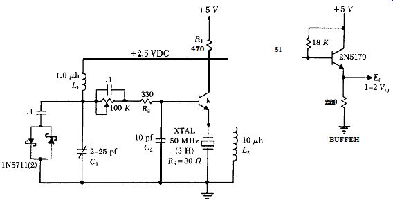
Fig. B.6 shows a 50 MHz circuit, also operating on the third harmonic.
To maintain the transistor's gain, note that the collector's load resistance R1 has been increased to compensate for the increase in the crystal's internal series resistance R,. The crystal's internal series resistance R, is 30 ohms, and its electrode shunt capacitance C, is 4.2 pf. The transistor's current gain
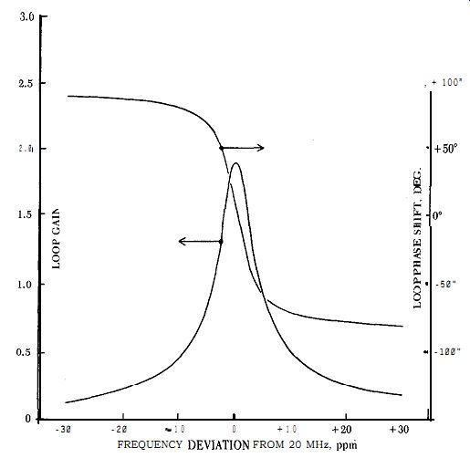
Figure B.4. Calculated loop gain and phase characteristics for circuit in
Fig. B.2.
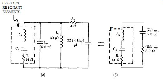
Figure B.5. External load seen by crystal's resonant elements in 20 MHz circuit:
(a) actual load, (b) equivalent series RC load.
Figure B.6. Emitter coupled harmonic oscillator at 50 MHz.
HFE is 100 (minimum), and reflects the 10 pf capacitance of C, as 1000 pf across the crystalin series with the transistor's internal emitter resistance r,. The transistor's internal emitter resistance r, is 30mV/5.3ma = 5.6 ohms. Using the same technique as shown in Figs. B.5a & b for the 20 MHz circuit, the equivalent series RC load seen-by the 50 MHz crystal in Fig. B.6 is 5.55 ohms (K)I~,~~ and 991 pf (Cshoad.
Fig. B.7 shows a 100 MHz oscillator, operating on the fifth harmonic.
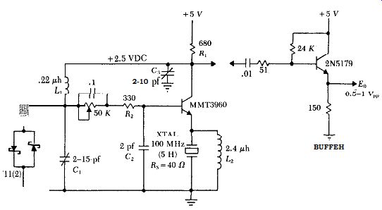
Figure B.7. Emitter coupled harmonic oscillator at 100 MHz.
... been increased, to compensate for the increase in the crystal's internal series resistance R,. This undesirable increase in R, as the frequency increases is a design drawback to the Emitter coupled harmonic circuit, and forms an upper frequency limit of about 100 MHz for good circuit operation. From shunt capacitance considerations, .it would be better to reduce R, as the frequency is increased.
An extra capacitor C, has been added to the 100 MHz circuit in Fig. B.7, from the transistor's collector to ground. Capacitor C3 is needed at frequencies above 50 MHz to tune out the shunting effect of inductor L,, on load resistor R,, so as to maintain a high load resistance for the transistor and get enough gain for oscillation.
The 100 MHz crystal's internal series resistance & is 40 ohms, and its electrode shunt capacitance C, is 5.7 pf. The transistor's current gain HFE is 100 (minimum), and reflects the 2 pf capacitance of C2 as 200 pf across the crystal, in series with the transistor's internal emitter resistance r,. The transistor's internal emitter resistance r, is 30mv/3.7ma = 8.2 ohms. Using the same parallel to equivalent series load technique as shown in Fig. B.5, the equivalent series load across the 100 MHz crystal in Fig. B. 7 is 7.7 ohms @had and 199.9 pf (C,J,<,,. The power dissipated in the crystal is less than 0.3 milliwatts.
B.3. PERFORMANCE
The three Emitter coupled harmonic circuits all perform very well. The waveform at the crystal is good. The circuits are relatively independent of changes in the 5V power supply, changing 2 ppm or less for a 2 volt supply ...
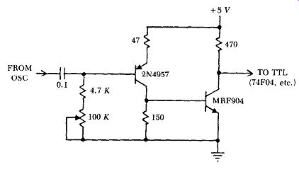
Figure B.8. Alternate digital buffer amplifier for driving TTL.
... change (4V to 6V). There are no parasitic effects when a good circuit layout is used.
A crystal's in-circuit Q is less than the crystal's internal Q by the ratio of the crystal's internal resistance R,, to the sum of the crystal's internal resistance R,? plus its equivalent series load resistance (Ra)road, ie, R,I(R + [R,],,,,,~).
At 20 MHz, the crystal's in-circuit Q is 14/(14 + 3.9) or 78% of the crystal's internal Q. At 50 MHz, the crystal's in-circuit Q is 30/(30 + 5.5) or 85% of the crystal's internal Q. And at 100 MHz, the crystal's in-circuit Q is 40/(40 + 7.7) or 84% of the crystal's internal Q. These are relatively high in-circuit Qs, which should give good short term frequency stability, and they do. The short term stability of the three circuits measured 0.1 ppm, at the limit of available measuring equipment. This stability is better than that of any other harmonic circuit tested.
B.4. APPLICATIONS
The isolation buffer amplifiers shown with the oscillators in Figs. B.2, B.6, & B. 7 are intended for sine wave output. An alternate digital buffer amplifier for driving CMOS or TTL circuitry at frequencies up to 100 MHz is shown in Fig. B.8. At frequencies below 50 MHz, a 2N5179 transistor can be substituted for the MRF904 in Fig. B.8.
In general, harmonic oscillator circuits do not have a wide frequency trimming range. The frequency can be trimmed by changing any of the phase leads or lags in an oscillator circuit. The frequency in Figs. B.2, B.6, & B.7 is trimmed by adjusting Cr, and is limited to 5-15 ppm maximum adjustment.
This can be increased to 25-60 ppm by putting a 35 pf variable capacitor in series with the crystal, and using it to trim the frequency. Above about 70 MHz, putting a variable frequency trimming capacitor in series with the crystal to get a wider trimming range also requires putting a small inductor directly across the crystal to resonate with the crystal's electrode capacitance C, and tune C, out of the circuit.
One side of the crystal is tied to ground in the Emitter coupled harmonic circuit. This makes it easy to put a varactor in series with the crystal, if desired, and operate the circuit as a voltage controlled oscillator (VCO). The maximum amount (in ppm) that a harmonic crystal oscillator can be pulled away from its normal oscillation frequency is limited, being inversely pro portional to the order of the harmonic used.
+++++++++++++++++++
FEEDBACK BRIDGE CIRCUIT
C.1. CONCEPT
The Feedback bridge is a simplified version of a circuit first described by Benjaminson. The basic simplified circuit is shown in Fig. (2.1. The crystal's internal series resistance R, and resistors R1, R, & RI,,,, form the four arms of a bridge. The L1C1 tank is series resonant at the frequency of oscillation, and converts the square wave output of transistor amplifier Q1 back into a sine wave, just as the resonant spring-mass elements within the crystal do. The L1Cl tank deliberately has a much lower Q than that of the crystal. At series resonance, the phase of the crystal's output voltage at point D is in-phase with the crystal's input drive voltage at point C. If the oscillation frequency moves away from series resonance, the phase of the output voltage at point D will either lead or lag the input drive voltage at point C, depending on whether the frequency moves down or up.
In Fig. C.1, the crystal and R_load form a voltage divider across the amplifier's output, and provide positive feedback to one of the amplifier's input terminals, the emitter of transistor Qr. Resistor R_load is also the crystal's load resistor, and for maximum in-circuit Q it should be kept small with respect to the crystal's internal series resistance R,5.
Bridge arms R, & R2 form a second voltage divider that provides negative feedback to the amplifier's other input terminal, the base of transistor Qr.
The negative feedback at point B is always in-phase with the amplifier's output square wave at point C, because the crystal's high Q holds the oscillation frequency at the center of L1C1's passband, where the phase shift through L1C1 is zero.
The advantage of a bridge circuit is that it can make the crystal's in-circuit Q higher than the crystal's own internal Q, thereby increasing the short ...
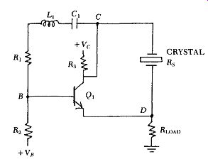
Figure C. 1. Basic circuit of simplified Feedback bridge oscillator. L1C1
is resonant at frequency of oscillation.
... term frequency stability. It does this by operating the crystal at series resonance, and subtracting out part of the crystal's resistive in-phase signal at the amplifier's input. The effect electronically increases the crystal's internal Q, which also reduces the short term frequency drift.
The crystal's in-circuit Q increases as more and more of the crystal's resistive in-phase signal is cancelled out. The subtraction of the two signals also reduces the net amplifier gain, so that the increase in in-circuit Q is limited by the amplifier gain available, which still has to exceed one around the amplifier loop for oscillation to occur. The characteristics of bridge circuits are discussed further in the sections on the Meacham and RLC half bridge circuits.
C.2. DESIGN
A Feedback bridge circuit at 1 MHz is shown in Fig. C.2. Fig. C.3 shows the waveforms at various points in the circuit of Fig. C.2. As Fig. C.2 shows, two emitter followers ( Q2 and Q3) h ave been added to the basic circuit. Q3 lowers the source resistance R, driving the crystal to 18 ohms. And Q2 isolates the crystal and its load resistor R_load from the negative feedback signal at point B, which also shows up by transistor action at Q1's emitter. The output impedance of emitter follower Q2 is made much lower than that of Q1, so that the AC voltage on 0,'s emitter is primarily controlled by the crystal's output voltage.
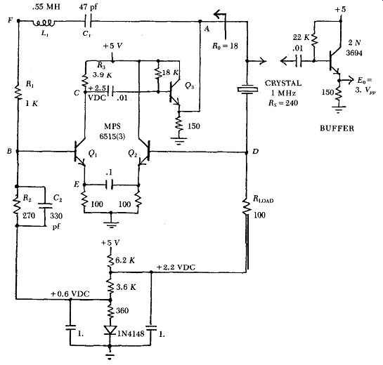
Figure C.2. Feedback bridge at 1 MHz.
Amplifier stage Q1 has a 40 degr. phase lag in it, partly because of the two collector to base capacitances (3.5 pf/each) across its collector load resistor Ra, and partly because of the large resistance value used for R3 to get a large amplifier gain. To let the crystal operate exactly at series resonance, the amplifier's 40 degr. phase lag is reduced to zero by putting a small capacitor C~ across bridge resistor Ra. The amplifier's phase lag could also have been eliminated by detuning C, slightly off series resonance with L,, but this sometimes generates a parasitic oscillation.
C.3. PERFORMANCE
The Feedback bridge gives outstanding performance. The crystal waveforms are good, and the frequency changes only 1 ppm when the power supply voltage is changed by 2 volts (4V to 6V). Its short term stability measured 0.1 ppm (or better), at the limit of available measuring equipment.
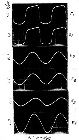
Figure C.3. Waveform circuit in Fig. 2
Transistor Q1 provides an in-phase gain of 28(cos 40 degr.) or 21X from emitter to collector. At series resonance, the amplifier's in-phase loop gain through the positive feedback bridge arms from point A to point D and back to point A is 5.9X. This is reduced by the amplifier's in-phase loop gain of 2.8X through the negative feedback bridge arms from point A to point B and back to point A, leaving a net positive loop gain for oscillation of 3.1X. The 2.8X gain reduction indicates how much of the crystal's total in-circuit resistance is being cancelled out, and therefore indicates how much the in-circuit Q is being improved. Without negative feedback, the circuit's short term stability measures 0.1 ppm. Dividing this by the 2.8 gain reduction of the negative feedback indicates that the short term stability with negative feedback should be .04 ppm, which is beyond the 0.1 ppm limit of the available test equipment.
To experimentally determine whether the electronic Q improvement is really there, the crystal's in-circuit Q was decreased by 10X, so as to reduce the circuit's short term stability down to something measurable with the available test equipment. The in-circuit Q was reduced in Fig. C.2 by inserting a 9 x (240 + 18) = 2322 ohm resistor in series with the crystal to increase its resistive losses 10 times, and by increasing the crystal's load resistor R_load from 100 ohms to 1000 ohms. With the negative feedback loop open (bridge arm R, disconnected at L,), the short term stability measured 0.3 ppm. With the negative feedback loop closed, the short term stability improves to 0.1 ppm. This 3X improvement in in-circuit Q by electronic means agrees reasonably well with the calculated 2.8X improvement, and shows that the concept of electronically subtracting out part of the crystal's in-circuit resistance does improve the in-circuit Q.
The improvement in short term stability is limited by the amplifier gain.
Adding a second amplifier stage would improve the circuit's short term stability considerably, but at the cost of increasing the parts count.
To calculate the crystal's in-circuit Q, the series equivalent of the parallel load on the crystal is needed, as shown in Figs. C.4a & b. From Fig. C.2, the external load seen by the crystal's internal resonant elements L, and C, ...
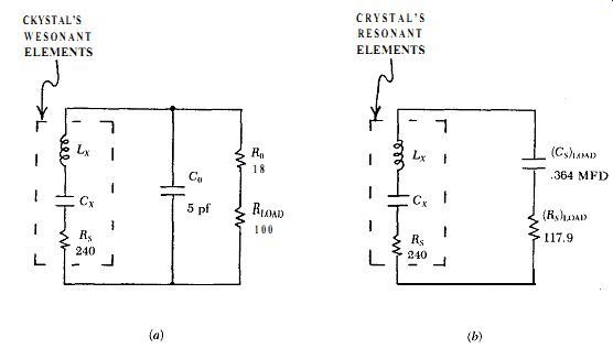
Figure C.4. (a) actual circuit load on the crystal's resonant elements, and
(b) the equivalent series RC load on the crystal.
... is approximated in Fig. C.4a by the parallel RC combination of the crystal's electrode shunt capacitance C, (5 pf) with the sum of the crystal's load resistor R_load (100 ohms) and the crystal's driving source resistance R, (18 ohms). Fig. C.4b shows that the equivalent series RC load on the crystal is 117.9 ohms and ,364 mfd. This gives an in-circuit Q without negative feed back of R,/(R, + [R,J,,J = 240/(240 + 117.9) or .67 of the crystal's internal Q. Multiplying this by the 2.8X gain reduction of the circuit's negative feed back gives an in-circuit Q with negative feedback of .67 x 2.8 or 1.9 times the crystal's internal Q.
The ,364 mfd of equivalent series load capacitance (Cs)load is in series with the crystal's internal capacitance C, of .00603 pf, and changes the crystal's resonant frequency proportionately. The crystal's resonant frequency will increase as the square root of the ratio of the original capacitance C, to the two capacitances combined in series, or equivalently, to the square root of one plus the ratio of the two capacitances, which is (1 MHz)[1 + (00603 x lo-r2)/(.364 x W")]" = .008 Hz. This is a negligible increase in the crystal's series resonant frequency.
The Feedback bridge can of course be used at other frequencies, assuming appropriate circuit changes are made. At a higher frequency such as 10 MHz, for example, an emitter follower would need to be added after Q3 to lower the crystal's drive resistance R, to a value less than the crystal's 5 to 10 ohm internal series resistance R, at 10 MHz. And something would have to be done to reduce amplifier Qr's phase shift, like using an LC tank (detuned off resonance) for the collector load on amplifier Q,. At a lower frequency such as 100 kHz, the phase correcting capacitor C2 probably would not be needed, which would usefully increase the amplifier's in-phase gain.
Also see: Link |