Some of the most important components in digital audio systems are the converters. Previous sections have shown the need for high resolution to obtain a satisfactory signal-to-noise ratio.
In video applications, an 8-bit conversion is more than sufficient. A 14-bit conversion (or an equivalent) seems a minimum for good audio performance and, for professional use, 16-bit conversion is required to leave a margin for further processing (e.g., filtering, mixing). In the PCM-F1 and compact disc system, 16-bit converters are used, while the PCM Video 8 system uses a 10-bit converter.
A/D converters
Fundamentally, A/D converters operate in one of two general ways. They either convert the analog input signal to a frequency or a set of pulses whose time is measured to provide a representative digital output, or compare the input signal with a vari able reference, using an internal D/A converter to obtain the digital output.
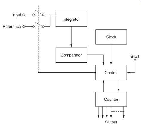
FIG. 1 Block diagram of a dual-slope integrating A/D converter.
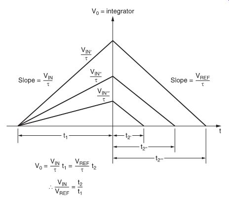
FIG. 2 Integrator output voltage as a function of time, during conversions.
Basic types of A/D converters
Voltage-to-frequency, ramp and integrating-ramp methods are the three leading conversion processes that use the time-measurement method. Successive approximation and parallel/modified parallel circuits rely on comparison methods.
Dual-slope integrating A/D converters The dual-slope integrating A/D converter contains an integrator, some control logic, a clock, a comparator and an output counter, as shown in FIG. 1. A graph of integrator output voltage against time is shown in FIG. 2.
The input analog signal is initially switched to the integrator, and the output of the integrator ramps up for a time t1. The slope of the ramp, and hence the integrator output voltage at the end of this time, depends on the amplitude of the analog input signal and the time constant t of the integrator:
So the integrator output voltage V0 at the end of time t1 is:
The reference signal is then switched to the integrator input, and the integrator output voltage ramps down until it returns to the starting voltage. The slope of the ramp during time t2 similarly depends on the integrator time constant and the integrator input voltage, this time the reference signal amplitude:
So the integrator output voltage at the initial time t2 is:
However, as these voltages are the same:
Therefore:
which shows that time t2 is totally dependent on the input signal amplitude, and independent of the integrator time constant.
By counting clock pulses during time t2 , a digital measure of the analog input signal's amplitude is made.
Average conversion time, i.e., the time the converter takes to perform the conversion of an applied input signal, is two clock periods times the number of quantization levels. Thus, for a 12-bit converter with a 1 MHz clock, the average conversion time is: 2 × 1 µs × 4096, or 8.192 ms. The precise conversion time, however, depends on the applied input signal amplitude.
Due to this long conversion time, integrating converters are not useful for digitizing high-speed, rapidly varying signals, although they are useful to 14-bit accuracy, offering high noise rejection and excellent stability with both time and temperature.
They can be modified to increase conversion speeds and are used mostly in 8- to 12-bit converters for digital voltmeters (DVMs), digital panel meters (DPMs) and digital multimeters (DMMs).
However, basic dual-slope integrating A/D converters are too slow for general computer applications.
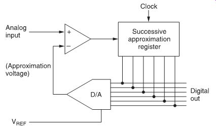
FIG. 3 Successive approximation A/D converter.
Successive-approximation A/D converters
The main reasons that the successive-approximation technique is used almost universally in A/D conversion systems are the reliability of the conversion technique, simplicity and inherent high speed data conversion. Conversion time is equal to the clock period times the number of bits being converted. Thus, for a 1 MHz clock, a 12-bit converter would take 12 µs to convert an applied analog signal.
A successive approximation converter consists of a comparator, a register, control logic and a D/A converter. The output of the D/A converter is compared with the input analog voltage (FIG. 3). Each bit line in the D/A converter corresponds to a bit position in the register. Initially, the converter is clear.
When an input signal is applied the control logic instructs the register to change its MSB to 1. This is changed by the D/A converter to an analog voltage equivalent to one-half the converter's full-scale range. If the input voltage is greater than this, the next most significant bit of the register becomes 1. If, however, the input is less, the next most significant bit remains 0. Then the circuit 'tries' the following bits through to the LSB, at which stage the conversion is complete. Thus, the number of approximations occurring in any conversion equals the number of bits in the digital output. FIG. 4 shows the operation of the successive approximation A/D converter graphically.
The main advantage of the successive-approximation converter is speed and this is limited by the settling time of the DAC.
Accuracy is limited by the accuracy of the DAC, and a high susceptibility to noise is its major drawback. As only one comparator is used and ancillary hardware is limited to logic, register and D/A converter, the successive-approximation technique provides an inexpensive A/D converter.
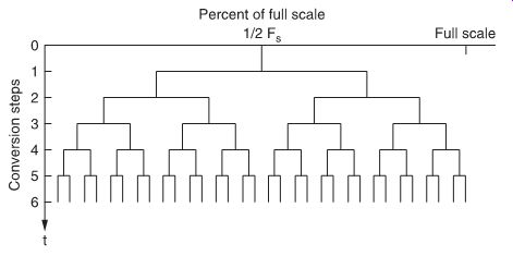
FIG. 4 Illustration of successive-approximation conversion. The digitally
generated voltage gets closer to the analog input voltage in a series of approximations;
each approximation is half the preceding one.
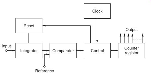
FIG. 5 Voltage-to frequency A/D converter.
Other types of A/D converters
Voltage-to-frequency converters
FIG. 5 shows a typical voltage-to-frequency converter. Here, the input analog signal is integrated and fed to a comparator.
When the comparator changes its state, the integrator is reset and the process repeats itself. The counter counts the number of integration cycles for a given time to provide a digital output.
The principal advantage of this type of conversion is its excel lent noise rejection due to the fact that the digital output represents the average value of the input signal. Voltage-to-frequency conversion, however, is too slow for use in data-acquisition system applications because it operates bit-serially (with a maximum of approximately 1000 conversions/s). Its applications are mostly in digital voltmeters (DVMs) using converters with resolutions of 10 bits or less.
Ramp converters
Ramp conversion works by continuously comparing a linear reference ramp signal with the input signal using a comparator (FIG. 6). The comparator initiates a counter when changing state and the counter counts clock pulses during the time the comparator is logically HIGH; the count is therefore proportional to the magnitude of the input signal. The counter output is the digital representation of the analog input.
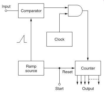
FIG. 6 Block diagram of a ramp converter.
This method is slightly faster than the previous one, but it requires a highly linear ramp source in order to be effective. It does offer good 8- to 12-bit differential linearity for applications requiring high accuracy.
Parallel A/D converters
Parallel-series and straight parallel converters are used primarily where extremely high speed is required, taking advantage of the fact that the propagation time through a chain of amplifiers is equal to the square root of the number of stages times the individual setting time, as opposed to adding up the times of each stage. By adding a comparator for every binary-weighted net work, as shown in FIG. 7, it is possible to take advantage of this higher speed. Parallel A/D converters are often called flash converters because of their high operating speeds.
The parallel A/D converter of FIG. 7 uses one comparator for each input quantization level (i.e., a 6-bit converter would have six comparators). Conversion is straightforward; all that is required besides the comparators is logic for decoding the comparator outputs.
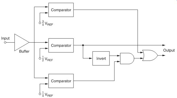
FIG. 7 Parallel A/D converter.
Because only comparators and logic gates stand between the analog inputs and digital outputs, extremely high speeds of up to 50 000 000 samplings/s can be obtained at low resolutions of 6 bits or less. The fact that the number of comparators and logic elements increases with resolution obviously makes this converter increasingly impractical for resolutions greater than 6 bits.
Modified parallel designs can provide a good tradeoff between hardware complexity and the resolution/speed combination at a slight addition in hardware and a sacrifice in speed. They can provide up to 100 000 conversions/s for up to 14-bit resolutions.
Sequential conversion (FIG. 8), for example, is often used for such applications. However, because of the increase in the number of comparators and the need to use an amplifier for every weighting network, cost is considerably more than that of a successive approximation.
The first 4-bit converter in the circuit in FIG. 8 provides the four most significant bits in parallel. These outputs are converted back to an analog voltage which is subtracted from the input.
The difference is applied to the next converter and the process is continued until the required 10 bits are obtained. This approach gives a reasonable tradeoff among speed, cost and accuracy.
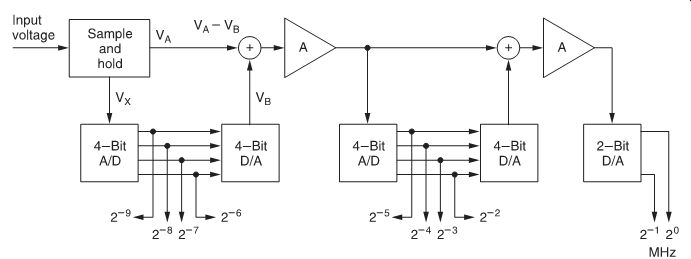
FIG. 8 Sequential parallel A/D conversion.
Delta-sigma modulator
A delta-sigma modulator is the key device in a 1-bit A/D converter. FIG. 9 shows a first-order delta-sigma modulator.
Operation is performed at each clock cycle, which corresponds to the oversampling frequency. At the beginning of each clock cycle, the differential amplifier outputs the difference between the input voltage V and the output voltage of the single-bit D/A converter. The integrator adds the voltage a to its own output from the preceding clock cycle. This voltage b is provided to the zero comparator. The output of the comparator will be logically HIGH or LOW, depending on voltage b being higher or lower than 0 V. The output then becomes a piece of single-bit A/D data, which is also used to determine the output of the 1-bit DAC for the next clock cycle. The 1-bit DAC outputs a positive full-scale voltage if its input is HIGH and a negative full-scale voltage if its input is LOW. Table 5.1 shows an example of actual operation in which the input is 0.6 V, with the full-scale voltage being ±1 V and all initial values 0.
The 1-bit A/D converter outputs only HIGH or LOW, which has no meaning in itself; this only becomes meaningful when a string of 1-bit data is averaged.
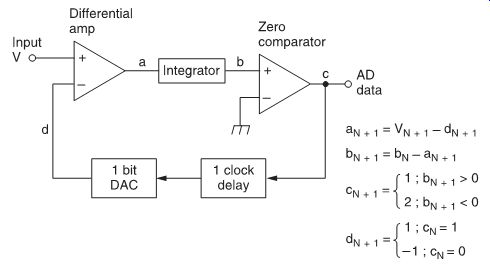
FIG. 9 First-order delta-S modulator.
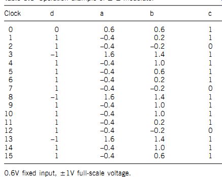
Table 1 Operation example of delta-S modulator
Because of the high sampling frequency (64 times oversampling) a very gentle low-pass filter can be used, resulting in low phase distortion. Compared to successive approximation A/D converters, single-bit A/D converters provide better performance while circuit complexity and cost remain equal.
Noise shaping
A delta-sigma modulator is sometimes also called a noise shaper because it passes signals and noise according to different transfer functions (FIG. 10). The signal transfer function for the modulator simplifies to:
This is the s-domain representation of a first-order low-pass filter. Deriving the noise transfer function for the same modulator produces:
This is the s-domain representation of a simple high-pass filter.
Plotting the transfer functions gives the result shown in FIG. 11. The signal is attenuated at higher frequencies, while the noise is shaped so that very little of its content is in the low frequency region. By using higher order delta-sigma modulators, the in-band noise can even be reduced further; however, out-of band noise will increase. In practice, a third- or fourth-order delta-sigma modulator is used to avoid stability problems while still using most of the noise shaping capabilities.
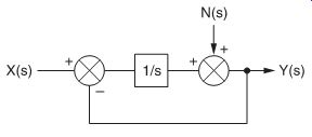
FIG. 10 delta-S modulator or noise shaper.
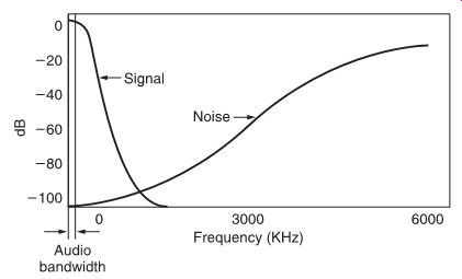
FIG. 11 Transfer functions of noise shaper.
High-density linear A/D converter
The A/D converter currently used in Sony R-DAT recorders and some MiniDisc recorders is the high-density linear converter. This converter uses two fourth-order delta-sigma modulators for simultaneous sampling of two audio channels. Its output is a serial data signal with 16-bit resolution coded in two's complement at a sampling frequency of 32, 44.1 or 48 kHz. The delta-sigma modulators operate at 64 times oversampling; for a system sampling frequency of 48 kHz, the analog audio signals are actually sampled at:
f s = 48 kHz × 64--3.072 MHz
This high sampling frequency eliminates the need for a sample hold circuit and a complex analog low-pass filter. A first-order RC network can be used as anti-aliasing filter because the audio signals do not normally contain frequencies above 1/2 f s (approx. 1.5 MHz). As a consequence, circuit complexity is greatly reduced.
The 1-bit stream, output from the delta-sigma modulators is hardly usable for further application. A built-in digital filter recalculates the single-bit input data at 64 f s to 16-bit words at f s. The so-called requantization is performed by the decimation filters.
FIG. 12 shows a block diagram of the high-density linear converter. This converter is clearly separated into an analog and a digital section. The analog part contains the voltage reference source and the delta-sigma modulators, while the digital part includes the digital filters, a controller and the output interface.
Each section has its own power supply to prevent digital noise from entering the analog signals.
During initialization, the converter performs an automatic calibration to compensate for possible offset errors in the converter itself. The analog inputs are grounded while the resulting output is measured and its value stored in SRAM as an offset. After calibration, the actual data are corrected by this offset value before being output.
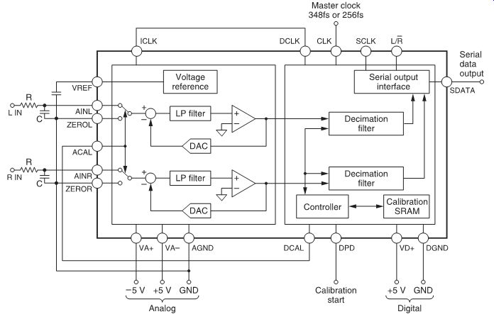
FIG. 12 High-density linear converter as used by Sony in digital audio
equipment.
With a harmonic distortion (THD) of less than 0.002% and a signal-to-noise ratio of more than 94 dB (EAIJ), the high-density linear converter is ideally suited for high-quality digital audio signal processing. This type of converter is used in all Sony's R-DAT recorders, such as DTC-77ES and DTC-59ES, as well as in the MDS-101 MiniDisc recorder.
D/A conversion in digital audio equipment
Weighted current D/A converter
The most common D/A converter in digital audio is the weighted current type. It consists of a series of electronic switches, each of which is connected to a current source. In an n-bit D/A converter there are n weighted current sources with a current value of 2(n -1) times the original current value 1. The current sources corresponding to the weight of the bit in the digital data signal are added to obtain a current that represents the value of the digital data. In fact, the digital data input directly controls the electronic switches that turn the current sources on or off. A current-to voltage amplifier converts the obtained current into a voltage before being output. FIG. 13 shows a typical block diagram of the weighted current type or current summing type D/A converter.
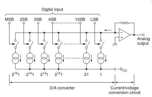
FIG. 13 Current summing type D/A converter.
Although this is basically a very simple converter, it has some serious drawbacks. The constant-current sources must be very accurately matched to prevent non-linear distortion. Suppose that the current 1 equals 0.1 mA, the constant-current source for the MSB should then deliver 2(n- 1) × 1 = 3276.8 mA or more than 3 A!
Moreover, to maintain 16-bit resolution the accuracy of the MSB constant-current source must be better than the current delivered by the LSB constant-current source.
Another type of D/A converter, more or less based on the same principles, is the ladder network type D/A converter as shown in FIG. 14. The so-called 'ladder network' is composed of resistors with values R and 2R to form a voltage divider. The electronic switches, controlled by the digital input data, change the output voltage of the voltage divider. The output voltage therefore represents the digital input signal. Accuracy is also a problem because all the resistors must be perfectly matched to ensure linearity. Temperature variations and ageing inevitably have a bad influence on the D/A converter linearity. The ON resistance of the electronic switches must be sufficiently low compared to the resistor value R to prevent it from having too much influence on the output signal.
Actual D/A converters are in fact a combination of a ladder network type converter with constant-current sources added for the upper and lower bits.
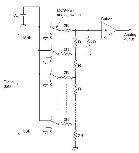
FIG. 14 Ladder network type D/A converter.
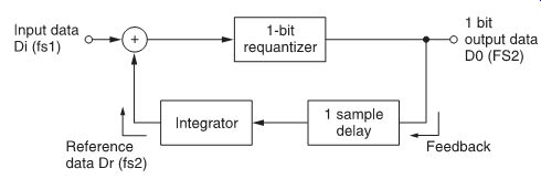
FIG. 15 Single-bit D/A converter.
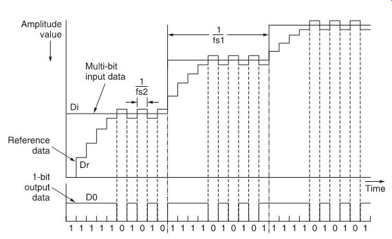
FIG. 16 Operation of the 1-bit requantizer.
Single-bit D/A converter
The disadvantages of the weighted current D/A converter can be overcome by using advanced laser trimming techniques to accurately match resistors and current sources. However, this has a negative influence on manufacturing costs. The single-bit converter makes high-precision D/A conversion possible without the need for expensive matched components.
FIG. 15 shows a block diagram of the single-bit D/A converter. The first step in the conversion process is the requantization of the multi-bit digital audio signal at f s 1 to 1-bit signal with a much higher sampling frequency f_s 2. Operation of the requantizer is explained in FIG. 16. The requantizer will determine whether the input data Di is higher or lower than the reference data (Dr ), the reference data being the requantized result of the previous input data. Whenever the reference data is lower than the input data, the 1-bit output of the requantizer will be 1 and the reference data will be incremented. This process is repeated for every block cycle of the sampling frequency f s 1. At a certain time the reference data will be higher than the input data. The resulting 1-bit data now becomes 0 and the reference data decremented. The output sequence 0-1-0 continues until new input data are applied to the converter.
The 1-bit output is converted to a pulse width modulation (PWM) or pulse density modulation (PDM) signal which, after low-pass filtering, represents the analog output voltage (FIG. 17).
Because of feedback of the reference data, the single-bit D/A converter acts as a noise shaper, similar to the single-bit A/D converter (FIG. 11). It shifts the requantization noise to the higher frequency regions, thereby lowering the quantization noise in the audible frequency range. Hence, the 1-bit D/A converter easily achieves a resolution of more than 16 bits in the audio frequency range. Non-linear distortion and DC offset are non-existing problems. The only major disadvantage is high frequency noise radiation caused by the high sampling frequency f s 2, which is usually several megahertz. A carefully designed single-bit D/A converter is therefore an inexpensive alternative for high-precision D/A conversion.
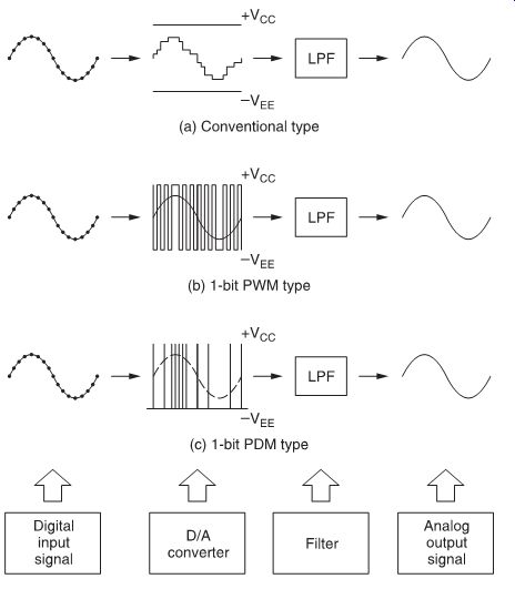
FIG. 17 Output signal of a conventional D/A converter (a), a 1-bit PWM
converter (b) and a 1-bit PDM converter (c).
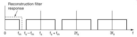
FIG. 18 Spectrum of a sample baseband audio signal. A filter must reject
all frequencies above a cut-off frequency fm.
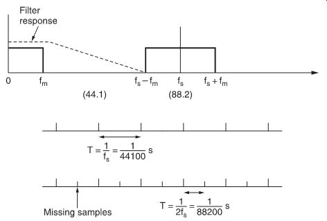
FIG. 19 In a ×2 oversampling system the effective sampling frequency becomes
twice that of the actual sampling frequency. A simple low-pass filter can be
used to reject all unwanted signal frequencies.
FIG. 20 Timing diagram of an oversampling system.
Words at a sampling frequency of 44.1 kHz have interpolated samples added, such that the effective sampling rate is 88.2 kHz.
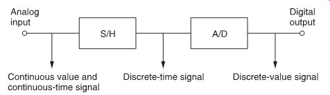
FIG. 21 How a continuous value and continuous time analog signal is first
converted to a discrete time but continuous value set of signals.
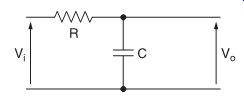
FIG. 22 Simple first order low-pass filter.
Oversampling
The output of a digital-to-analog converter cannot be used directly; filtering is necessary. The converter output produces the frequency spectrum shown in FIG. 18, where the baseband audio signal (0-f m) is reproduced symmetrical around the sampling frequency (f s ) and its harmonics. The low-pass reconstruction filter must reject everything except the baseband signal.
A sampling frequency (f s ) of 44100 Hz and a maximum audio frequency (f m) of 20 000 Hz mean that a low-pass filter with a flat response to 20 kHz and a high attenuation at f s - f m (44 100 - 20 000 = 24 100 Hz) is needed. An analog filter can be made to have such a sharp roll-off, but the phase response will introduce an audible phase distortion and group delay.
One approach to getting round this problem is oversampling. Oversampling is the use of a sampling rate greatly in excess of that stipulated by the Nyquist theorem. Practical implementations use a ×2 oversampling (f s = 88.2 kHz) or a ×4 oversampling frequency (f s = 176.5 kHz). The output spectrum of the D/A converter in a ×2 oversampling system is shown in FIG. 19, where the large separation between baseband and sidebands allows a low-pass filter with a gentle roll-off to be used. This improves the phase response of the filter.
Digital words are input at the standard sampling rate of 44.1 kHz (i.e., no extra samples need be taken at the A/D conversion stage), and extra samples are generated at a rate of 88.2 kHz (FIG. 20). The missing samples are computed by digital simulation of the analog reconstruction process. A digital transversal filter (also known as a finite impulse response filter) is well suited for this purpose.
Analog versus digital filters The discrete-time signal produced by sampling an analog input signal (FIG. 21) is defined as an infinite series of numbers, each corresponding to a sampling point at time t = Tn for -8 < n < +8. Such a series is always referred to by its value at t = Tn which is x(n).
The series x(n) is defined as:
x(n) = …, x(-2), x(-1), x(0), x(1), x(2), … with element x(n) occurring at time t = Tn.
Analog filters
The first-order low-pass analog filter shown in FIG. 22 is often described as a function of s, the independent variable in the complex frequency domain. The transfer function of such a filter is given by:
...where...
? = angular frequency = 2pf and ?0 is the angular frequency at the filter's cut-off frequency f c = 1/RC.
Knowing this, the cut-off frequency of the filter can be calculated as follows:
so:
Digital filters
A digital filter is a processing system which generates the output sequence, y(n), from an input sequence, x(n), where:
present and past past input output samples samples
The coefficients a0 , a1 , …, aM and b0 , b1 , …, bN are constants which describe the filter response.
When N > 0, indicating that past output samples are used in the calculation of the present output sample, the filter is said to be recursive or cyclic. An example is shown in FIG. 23. When only present and past input samples are used in the calculation of the present output sample, the filter is said to be non-recursive or non-cyclic: because no past output samples are involved in the calculation, the second term then becomes zero (as N = 0).
An example is shown in FIG. 24.
Generally, digital audio systems use non-recursive filters and an example, used in the CDP-102 compact disc player, is shown in FIG. 25 as a block diagram. IC309 is a CX23034, a 96th-order filter which contains 96 multipliers. The constant coefficients are contained in an ROM look-up table. Also note that the CX23034 operates on 16-bit wide data words, which means that all adders and multipliers are 16-bit devices.
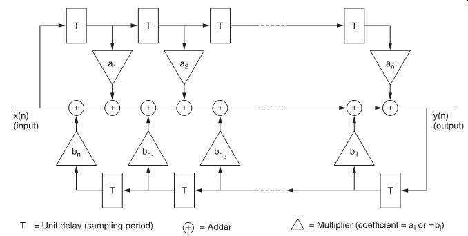
FIG. 23 Recursive digital filter.
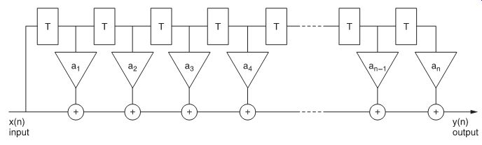
FIG. 24 Non-recursive digital filter.
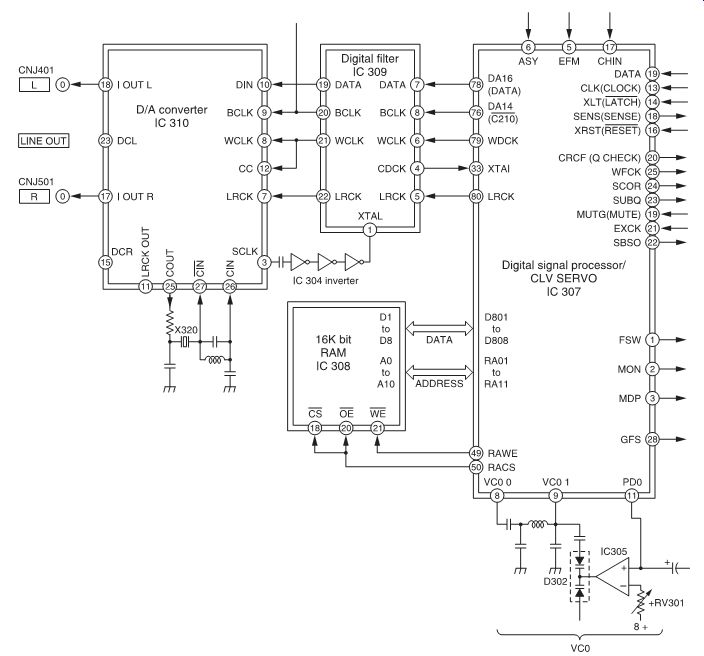
FIG. 25 CDP-102 digital filter.