One-chip voltage splitter conserves battery power
by David Bingham Intersil Inc., Cupertino, Calif.
Positive and negative supply voltages of equal magnitude are usually secured in a battery or other low-power floating-source arrangements by establishing system ground at half the source potential by means of a simple voltage divider. But this scheme more often than not consumes excessive power. Modifying Intersil's ICL7660 positive-to-negative voltage converter to work as a voltage divider, however, will increase the power-conversion efficiency to as high as 98% at an output current of 10 milliamperes.
The conventional voltage divider circuit shown in (a) uses two resistors and a unity-gain operational-amplifier buffer. While this circuit can function at relatively low power, depending upon the op amp used and the value of R, it will suffer from an inherently low power efficiency if the load should be connected between system ground and either V+ or V. In such cases, the current flowing through the load will always be the same as that drawn from the battery, and thus the maximum efficiency can never be greater than 50%.
The ICL7660 can be made to simulate a divide-by-2 voltage converter by simply grounding pin 5 (normally the V- lead) and using the normally grounded lead at pin 3 as the output, as shown in (b). The voltage distribution on the chip will be unchanged, since pin 3 is midway between V+ and V-, as before. And no power is lost in heating up any resistance, as the ICL7660 operates in the switched-capacitor (charge-transfer) mode to derive the output voltage.
With this configuration, an open-circuit output voltage equal to V/2 ±0.1% is achieved. The output impedance is 13 ohms for a supply voltage of 9 V and 0.1 mA <1.1<80 mA, or 17 ohms for V = 6 v and an output current in the same general range.
Because the ICL7660 can source only an output current reliably, difficulty may be encountered if the load is connected between pins 3 and 8 of the device. To ensure startup for current-sinking applications, a 1-m0 resistor is placed between pin 6 and ground. This step guarantees that there will always be some voltage across the on-chip oscillator and the control circuitry.
As for circuit performance (c), conversion efficiency will be no lower than 80% for V = 6 V and 0.5 MA < lout < 80 mA. In equation form:
n = (V,1,,t/V+I+)100 where is the magnitude of the output current, regard less of sign.
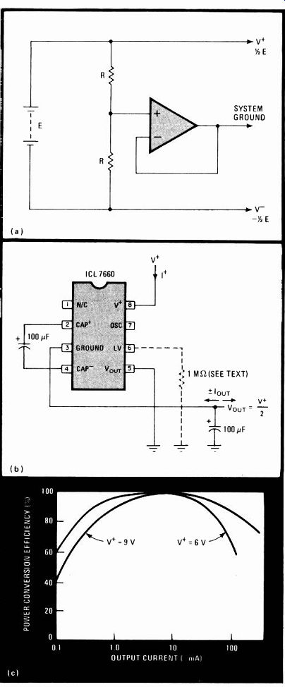
Efficient. Simple resistive voltage divider (a) dissipates excessive power and thus is ordinarily not suited to providing positive and negative supply voltages from floating source. Suitably wired CL7660 converter (b) provides the function without power loss, yielding conversion efficiencies (c) approaching 98%.
V-MOS oscillator ups converter's switching frequency
by Bill Roehr Siliconix Inc., Santa Clara, Calif
The benefits of switching a flyback converter at high frequency to increase its efficiency and minimize its size may be realized by employing a V-groove mos field effect transistor as its power oscillator. Unlike bipolar power transistors, where storage-time effects hamper device turn-off, the turn-on and turn-off times for v-mos units are fast- typically a few nanoseconds. Thus, switching speeds of 250 kilohertz can easily be achieved.
The circuit configuration is very simple, as shown.
When the circuit is first energized, a positive voltage is capacitively coupled to the gate, turning on the VNIOKM v-mos device. Enhancement voltage is maintained by the potential across the transformer's primary, which is reflected onto its feedback winding. The FET continues to conduct until the core saturates, whereupon the feedback voltage collapses and turns the device off.
With the FET off, energy stored in the magnetic field surrounding the primary winding is transferred to the secondary winding. Zener diode D, clamps the primary winding voltage to the desired potential and limits the voltage across the v-mos gate to some value below its 60-volt breakdown rating. The energy transferred to the feedback winding has the proper polarity to hold the FET in cutoff. When the transformer comes out of saturation, the operating cycle repeats. Diode D2 prevents negative spikes from damaging the gate of the FET. Resistor R1 suppresses any parasitic oscillations caused by switching.
Energy transferred to the secondary winding delivers power to filter capacitor C2 via rectifying diode D3. A single 4.7-µF capacitor provides sufficient filtering at the 250-kHz operating frequency. The dc output voltage may be made positive with respect to the main rail by grounding terminal 1 and negative with respect to the main rail by grounding terminal 2.
A dc output of up to 60 v can be developed by simply selecting a zener diode of that same value, although practically any voltage can be obtained by altering the transformer's turn ratio. The supply voltage should be set between 3 and 5 v dc.
Note that the physical size required for this flyback converter will be minimal, since the reactive components will be small and light because of the high operating frequency.
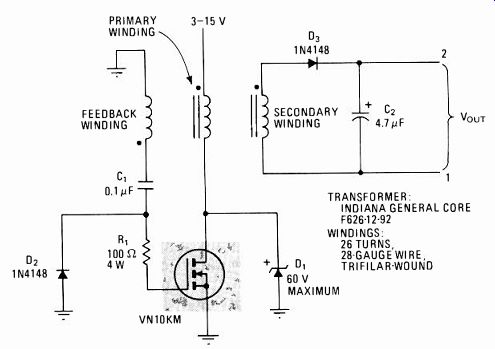
--- High-flying. V-MOS power-FET converter easily operates at switching
frequencies of 250 kHz and can work up to several mega cycles, thereby
increasing the efficiency of the flyback converter and also minimizing
its size. Dc output potentials of up to 60 V may be ordered by appropriate
selection of zener diode D1.
Low-loss shunt protects high-current supplies
by Roy Hartkopf and Ron Kilgour Alphington, Victoria, Australia
The usual method for providing short-circuit protection in low-voltage, high-current power supplies is to employ a current-sensing resistor in series with the load. Unfortunately, this scheme develops an appreciable voltage drop across the resistor when large currents flow and may consequently reduce the available output voltage to a great degree. The voltage drop can be virtually eliminated with an alternative method, shown here, which uses an audio transformer and a single-turn winding to sense the overcurrent condition at the secondary of the supply's power input transformer. Besides being inexpensive, the current sensor will react faster to overloads than some of the more conventional circuits.
As shown in the figure, current protection may be secured for a typical 27-volt, 20-ampere supply by winding a single turn of 10-gauge wire, which is placed in series with the power transformer's secondary and the supply's rectifier bridge, onto a small audio transformer connected in the control section of the supply. During normal operation, transistor Q1 will be saturated because current is delivered to its base from the 27-v supply line.
Note that the secondary of the audio transformer, in conjunction with diode D1, will contribute a relatively small negative voltage at the summing junction of P1.
Should the current demands increase, however, the magnitude of the negative voltage developed at the audio transformer's secondary will increase and, consistent with the setting of potentiometer PI, pull the base to-emitter voltage down to cut off Q1. The 2N2646 unijunction transistor will then turn on and trigger the silicon controlled rectifier, and the control signal will be brought low. Thus this signal can be used to cut off the supply. This action will be instantaneous, occurring on the first overload cycle.
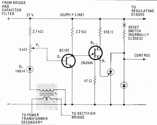
-------- Current gauge. An audio transformer and a single turn of
heavy-gauge wire, placed between input transformer's secondary and rectifier,
give high-current supplies overload protection without introducing input-to-output
voltage drop that occurs with units employing current-sensing resistors.
Potentiometer P1 sets the overload point.
Overload detection is instantaneous, occurring on the first positive cycle of input voltage.
Low-cost timers govern switched-mode regulator
by Luces M. Faulkenberry Texas State Technical Institute, Waco, Texas
This step-down switching power supply, which uses 555 timers for pulse-width modulation, combines good performance with very reasonable cost. Providing an output of 12 volts at 1 ampere for an 18-v input, the unit offers input-current limiting, 0.1%/v line regulation, 0.5% load regulation, and an output ripple of only 20 my. however, the design equations given here enable the user to specify his own requirements. The supply can be built for less than $15.
Operating as an astable multivibrator at 20 kilohertz, timer A1 generates the trigger pulses needed to switch the output of monostable multivibrator A2 to logic 1 during each cycle. Modulating the control pin of one-shot A2 with the output of the 741 operational amplifier controls the width.
The op amp compares a preset fraction of the supply voltage, Vout', with the 6.8-v reference, Vref. When Vref>Vout, the control pin of the one-shot moves high and each pulse from the output of A2 is lengthened accordingly until the reference and supply voltages are virtually equal. Similarly, if Vref< Vout, the output pulses are shortened.
As seen, transistors Q1 and Q2 in the simple feedback loop perform the switching function. Monitoring transistors Q3 and Q4 limit the current by bringing A2's reset pin low when the design-maximum peak current through the inductor is reached, thereby shortening the width of the output pulses until the cause of the trouble is removed. Q3 can also serve in a dual capacity as a switch to turn off the supply during overload conditions. For example, should automatic shutdown of the supply be necessary, Q3 could be used to fire a silicon controlled rectifier in order to hold the reset pin of oscillator A1 low permanently. In these cases, a simple circuit would also be needed to reset the supply manually.
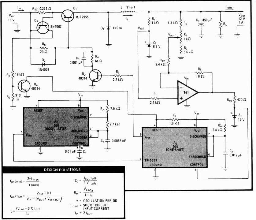
----------- Rudimentary. Dc-dc switching regulator, using 555 timers,
is simple and low-cost yet provides good performance. Typical specs of
18 V-in-to-12-V-out unit include 0.1%/V line regulation, 0.5% load regulation,
and output ripple of 20 mV. User can design supply to meet his own requirements
with aid of given equation set.
Low-power inverter ignites gas-discharge lamps
by Akavia Kaniel Measurex Corp., Cupertino, Calif.
This inexpensive low-power inverter generates the high voltage required to ignite gas-discharge lamps of the mercury-vapor type and supplies the small current needed to maintain conduction. It also prevents the deposition of ions on the lamp's cathode that tends to shorten its operating lifetime. Using one integrated circuit, an operational amplifier, and two field-effect transistors, the inverter can be built for less than $30, including the cost of the unit's pulse transformer.
As shown, the SG3524 pulse-width modulator and transformer T1 convert a 24-volt dc input into the 1,500 v potential required for turning on the Ultra Violet Products 11SC2 lamp. When switch S1 is closed, the chip's E. output goes high, thus inducing a high-voltage square wave across T1's secondary.
As current begins to flow in the primary, feedback amplifier A1 comes into play. Detecting the relative magnitude of the current through the 0.2-ohm sense resistor, AI automatically sets the width of the 20 kilohertz modulating pulses so that a constant ac current of 5 milliamperes is delivered to the lamp. Use of a push-pull output and the balanced transformer connection ensure that the switched square wave is symmetrical about the zero axis. This ac driving signal thus prevents the migration and subsequent buildup of ions around the lamp's cathode.
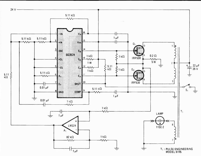
Arc-over. Low-power transistor-driven inverter generates high-voltage
square wave to fire fluorescent and mercury-vapor lamps and provides
low current to maintain ionization. Symmetry of inverter's output prohibits
build-up of ions at lamp's cathode, thus increasing operating life.
Reed-coil relay is behind flexible fault detection
by Daniel Appiolaza, Mendoza, Argentina
Mechanically providing such functions as undercurrent and overcurrent protection for power supplies and fault indication for an automobile's turn signals or stoplights is easier to achieve inexpensively with relays having a separate reed and coil. Using the coil as a remote current-sensing device also makes the relay flexible enough to do a myriad of other jobs not possible with self-contained units.
Consider the example of current-overload monitoring (a). Here, the normally open reed switch serves to activate the shunt formed by the light-emitting diode, resistor R1, and the zener diode when excessive supply current flows.
The coil, made from four turns of No. 12 gauge wire, is tightly wound over the reed so that an instantaneous line current equal to or larger than approximately 5 amperes dc will close the reed relay and trigger zener diode D. Thus the reference voltage will drop to zero until the line current is reduced and the reset switch is depressed.
A second example is the fault detector of an automobile's brake signals (b), where it is important to know when a stop or turn lamp has failed (a feature not supplied by auto makers). Here, two reed/coil assemblies are required, with the reed contacts being normally closed.
If for any reason either of the stoplights does not turn on when the brake is applied, no current can flow through either coil. Consequently, the reed switches will not open and the panel LED will indicate trouble with the signaling system.
With normally closed relay contacts, however, the stoplights may still turn on despite a failure in the reed circuit or even the LED/resistor itself. Alternatively, it might be better if the reeds are of the normally open type. Then the circuit can be wired to switch on the panel LED only when the car's stoplights become active.
This latter arrangement will positively indicate a failure in the system. If the LED does not turn on when the brake is applied in the normally open reed system, however, it dries indicate difficulty with either the lamp or the monitor circuit.
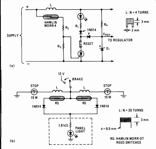
------------ Switching separates. Two-element relay having remote four-turn current-sensing coil and normally open reed switch (a) provides inexpensive overcurrent protection for power supply. When implemented in car's brake-signal system, relay detects faulty turn or stoplights. A normally open relay circuit might be preferable to the normally closed configuration shown.
Milliampere current source is voltage-controlled
by William J. Mundl Concordia University, Department of Psychology, Montreal, Canada
The constant small positive or negative current produced by this voltage-controlled source is useful for a variety of low-level measurements. As the current also has a virtually linear relationship with the input voltage, it may be modulated as desired by a given input waveform or, still more usefully, be put under microprocessor control to create an automated test system.
As seen in (a), incoming signals in the range of 0 to 10 volts are buffered by the LM358 micropower operational amplifier A1 and then introduced to A2, which with transistor Q, makes the current-monitoring feedback circuit. For a given input voltage, A2 amplifies and inverts Q1's emitter-to-base voltage variations, so that any increase or decrease in current due to temperature or load variations is counteracted. As a result, the current will rise linearly from zero to where I, is determined by resistor R, with the variation of I for a given V,. being about 2%. In this circuit, the maximum attainable value of L is approximately 4 milliamperes, obtained with a 1.5-kilohm load impedance.
Calibration of the circuit is simple. Potentiometer R, need only be adjusted to null the output current for V = 0. For convenience in setting the output current, an oscilloscope can be placed across a 1-W resistor.
The layout for this circuit's counterpart, a negative current sink, is similar, as shown in (b). (:), becomes an npn transistor, the supply potential on the circuit is reversed, and an inverting stage is added at the input.
Although the circuit is relatively insensitive to variations in the supply voltage, use of a regulated power supply of the simple series type is recommended.
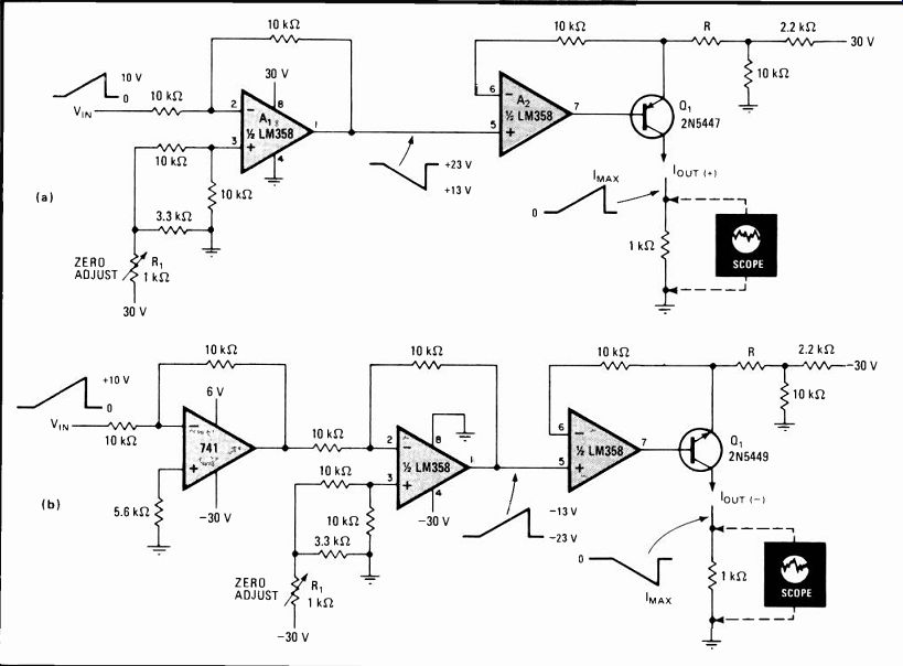
---------- Milliampere magnitudes. The circuit's input voltage sets
its constant output current to within 5% of the desired value, adjustable
from 0 to 4 mA if R = 1.5 kit. Its linear response makes it attractive
for microprocessor-based (automated) tests and measurements. The positive
source in (a) or negative sink in (b) is simply calibrated by means of
resistor R, and an oscilloscope monitor.
Power-fail detector uses chip's standby mode
by Jerry Winfield Mostek Corp., Carrollton, Texas
As microprocessors are used more frequently for consumer and industrial applications, the need to preserve data and program status during power outages has become increasingly important. Until now, this function has been implemented with a small, outboard complementary-MOS random-access-memory battery-charging circuitry, power-fail circuitry, and a battery.
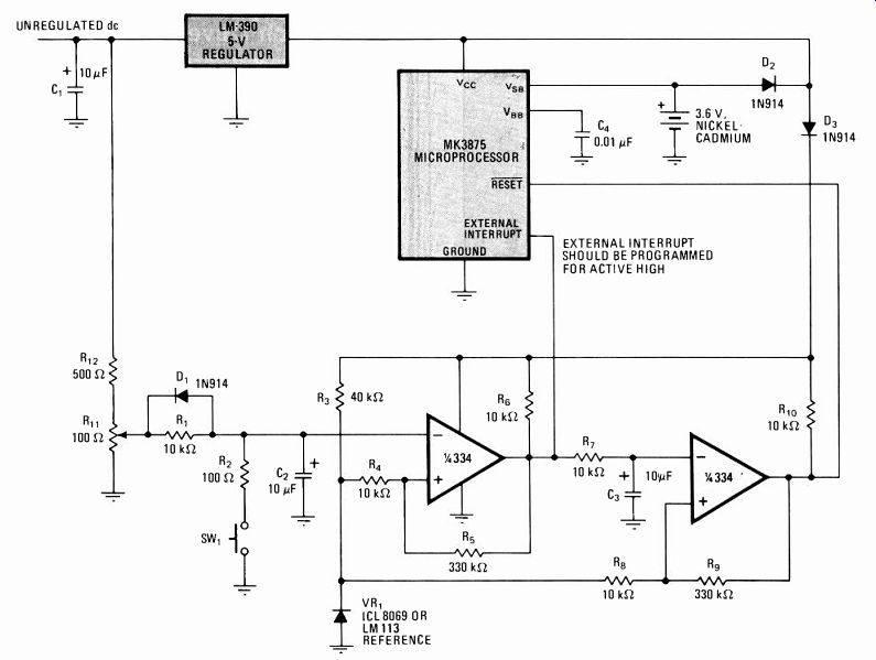
----------- 1. Please stand by. Though primarily for detecting power failures, this circuit also adds power-on and push-button reset functions to the MK3875 microcomputer, which has 64 bytes of standby RAM and a battery-charging circuit for implementing a standby power mode.
The MK3875, one of the MK387X family of single-chip microcomputers, simplifies the job of providing a battery backup system by incorporating 64 bytes of standby RAM and the battery-charging circuit onto the microprocessor chip. The only external components required are a battery and the power-fail circuit.
Figure 1 shows a simple, low-cost power-fail-detection circuit that can be designed with readily available parts.
Figure 2 details the timing relationship between RESET and V for enabling and disabling the standby RAM function. Simply stated, RESET must be low when V is below its specified voltage, which is 4.75 volts for a 5% part and 4.5 V for a 10% part.
The circuit shown in Fig. 1 detects power failures and resets the device automatically at power-on and manually during operation. The circuit monitors the unregulated voltage that feeds the V© regulator and compares this voltage against a voltage reference. When the voltage drops below the reference, the RESET line is pulled low. Hysteresis is designed into the comparator to pre vent the oscillation caused by slow rise and fall times.
The trimming potentiometer, R11, should be adjusted so the negative threshold voltage Vu,_ is greater than the minimum input voltage of the V regulator. Adjusting the threshold voltage above the minimum will yield additional time before the RESET line goes low should the external interrupt be used for saving variables.
As mentioned earlier, the circuit also functions as a power-on or manual reset. The power-on reset is created by the addition of C2 and D1, and the manual reset is created by the addition of R2 and SW1.
The power-fail circuit can also be configured to generate an external interrupt to the MK3875 to save variables before the RESET line is activated. Adding capacitor C3 allows time for executing the save routine before the RESET line is pulled low; the external interrupt should also be programmed as an active-high input.
The MK3875 was designed primarily for use with a small 3.6-v nickel-cadmium battery and will automatically supply a maximum charging current of 19 mA at 3.2 v and a minimum trickle charge of 0.8 MA at 3.8 V.
The size of the battery will depend on the length of required standby time. (With a V variation of 4.75 to 5.25 v, the standby current for the RAM will vary between 3.7 mA to 6 mA.) Among those battery manufacturers whose small nick el-cadmium batteries could be used with the MK3875 are Varta, Yuasa, General Electric, Gould, Sanyo, and Panasonic.
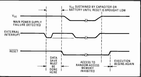
-------------- 2. Wave goodbye. Where a save routine is needed to
preserve critical data before power is lost, the external interrupt must
be toggled before the reset line, during which time the routine is executed.
The time allowed to save the data is determined by the value of C3.
High-current voltage regulator works with negative supplies
by Robert A. Pease National Semiconductor Corp., Santa Clara, Calif.
Monolithic voltage regulators combine the voltage stabilizing and power-protection circuitry of discrete component designs into a single package. As a result, current-limiting, voltage-limiting, and even thermal limiting features are built into the regulating function and therefore require no further consideration by the designer. Unfortunately, most high-power monolithic voltage regulators are intended for positive-supply voltages.
Currently, the only negative-voltage monolithic regulators that are available are those with 1.5 or 3 amperes of rated output current. The LM337 adjustable and LM345 fixed-5-volt regulators are two such devices.
New high-current monolithic regulators, such as the LM338, rated at 5 A, and the LM396, rated at 10 A, are normally characterized as positive regulators. Yet they can also be used in applications calling for negative regulators, such as in an emitter-coupled-logic computer where several amperes at-2 v are often required.
The figure shows an LM396 that is controlled by an LF351 operational amplifier that holds the LM396's adjust pin at 1.25 v below the -5.2-v bus.
The accuracy of the output voltage depends on the -5.2-v supply, which is used as a reference. Short circuit limiting to 15A and thermal-limit protection to 170°C are provided by the LM396. Although the -12 v dc need not be closely regulated, it must be present or else the -2-v supply will fall toward -3 or -4 v, which is excessively negative.
Similarly, a positive regulator such as an LM338 or one or more LM396s have been used to regulate 5, 10, 20 A, or more of -5.2 v dc when a 9-v dc power and a -15-v dc bias supply are used.
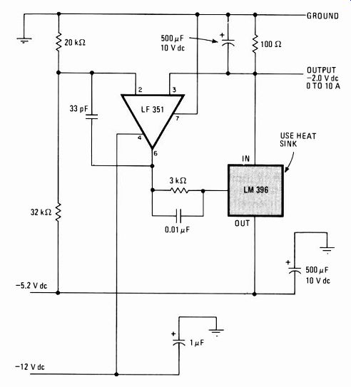
--------- Both ways. An LM396 monolithic positive-voltage regulator can be used, as shown here, to regulate a 10-ampere negative supply. Feedback to the regulator chip is furnished by an LF351 operational amplifier.
The LM396 regulator provides full short circuit protection to 15 A, as well as temperature protection to 170°C.
Regulator boosts supply voltage for programming EE-PROMs
by Henry Fung and John Rizzo Intel Corp., Special Products Division, Santa Clara, Calif.
The 2816 is a new electrically erasable programmable read-only memory in which writing and erasing can be accomplished on board by feeding a 21-volt dc pulse to the chip's Vpp pin. But generating the pulse requires a power supply with an output voltage of + 24 v dc, which is then clamped by a zener diode to about + 21 v dc.
When that is not available, a switching regulator can be used to convert the commonly available + 5 v dc into + 24 v dc. The advent of large-scale integration technology simplifies the design of such a dc-to-dc converter.
Figure 1 shows the circuit diagram for a voltage converter using a TL497 switching voltage regulator that is very inexpensive to build.
The circuit operates as follows: the frequency at which transistor Q, is switching is determined by capacitor C1.
The converter's output voltage is fed back to an internal comparator that controls the on and off time of Q1.
When Q1 is turned off, the voltage across the inductor inverts, and the blocking diode, D1, is forward-biased to provide a current path for the discharge of the inductor unto the load and filter capacitors (C2 and C3). While Q1 us turned on, the current into the inductor increases linearly. D1 will then become reverse-biased and the output load current will be provided by the filter capacitors. But current output above 80 milliamperes will cause the output-voltage regulation to degrade.
The switching-regulator efficiency may be calculated as a ratio of output power to input power (including a 50% duty cycle). Therefore: efficiency (%) =output power x 100% input power
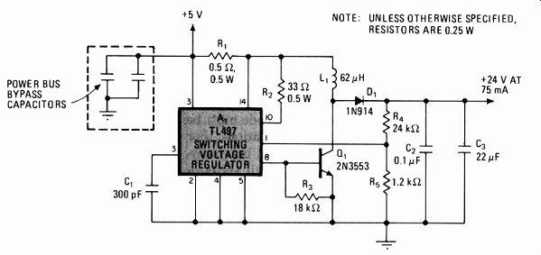
----- 1. Big boost. A dc-to-dc converter based on a TL497 switching
regulator boosts a 5-V supply voltage to 24 V dc for programming electrically
alterable read-only memories. Q1 is switched at a rate deter mined by
C1, and the induced voltage in L1 is the output.
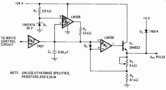
------------- 2. Sensing switch. The programming voltage, Vpp, is
applied when the output of A2, an open collector gate, is high for 10
ms during a write cycle. C, charges up and ultimately turns on Q,, which
provides up to 75 mA of drive to erase or write into a memory.
24 v x 80 mA -5 v X1,160 mA X0.5X100% = 66%
The output voltage from the switching regulator may now generate the Vpp pulse required to program the 2816 EE-PROM. The next requirement is a circuit that switches the 24 v on during write and erase cycles (Fig. 2) DI suppresses any noise on the 24-v line and clamps the line at about 21 v. A2 is an open-collector gate and when its output is low, C1 and pin 5 of A3 will be shorted to ground. Therefore, Q1 will be turned off and the Vpp pulse will stay at a level equal to the 5-v supply voltage less one diode drop. When a write cycle is initiated, the output of gate A2 will be high for 10 milliseconds, allowing C, to charge. The time constant, determined by R2 and C1, is 600 microseconds. As soon as the capacitor is charged up to the zener diode voltage, the feedback amplifier will force this voltage to remain constant. The final output voltage is adjusted by R3. Q1 provides the additional current-drive capability up to 75 mA. Diode D2 across pins 5 and 6 of A3 ensures a Vpp pulse that will be glitchless.
The 2816 has an inhibit mode that allows the device to be deselected during programming. Consequently, only one switch is needed for many devices in a system.
However, the Vpp switch must still supply the 1pp standby current for the unselected devices.
The circuit has been tested over the 2816's full operating temperature range.
Stacked voltage references improve supply's regulation
by Wes Freeman and George Erdi Precision Monolithics Inc., Santa Clara, Calif.
By combining low-cost precision voltage references, inexpensive yet accurate power supplies that work over a wide range of voltages may be built. When suitably stacked, these voltage references even improve the regulating performance of the supply.
Consider the circuit in Fig. 1, which can be built for approximately $10. It uses two 10-volt references so combined that the supply will work over a range of 0 to 20 v, with switch S1 selecting the 0-to-10 -and 10- to-20-v ranges.
An operational amplifier isolates potentiometer R1 , which sets the output voltage to within 300 microvolts of the desired value. The op amp's short-circuit current, approximately 22 milliamperes, limits the maximum base current available to the power transistor. As a result, the maximum available output current is nearly 1 ampere.
The supply's line regulation is within 0.005% of scale reading per volt in the 10-to-20-v range. In the 0-to-10-v range, line regulation is significantly improved to within 0.0001%/v and is mainly limited by the op amp's supply rejection ratio because the output of the second reference regulates the line voltage of the first.
Load regulation is determined by the change in the op amp's open-loop gain versus load current. In this circuit, measured values were ± 0.001%/A in the 0-to-800-mA range. Output voltage drift due to temperature is ± 0.002% of scale reading per °C.
At an increase in component count and hence also in cost, the performance of the supply may be improved appreciably, as seen in Fig. 2. The addition of a third reference regulates both the 0-to-10- and 10-to-20-v ranges. A Darlington power-output transistor permits a 4-A load current.
As a result, the total change in output voltage is less than ± 0.001% for a change in load current of 0 to 2 A and a change in line voltage ranging from 33 to 59 v.
Potentiometers R2 and R3 adjust the output voltage for the 10-v and 20-v ranges, respectively, while R4 nulls the op amp's offset voltage.
The substitution of a highly linear precision potentiometer and turn-counting dial for R1 permits a dial accuracy of ±2 my from 0 to 20 v, with a resolution of 200 µv. Moreover, if a better grade of reference (REF- 01) is employed, the temperature coefficient is ± 0.001% of scale reading per °C.
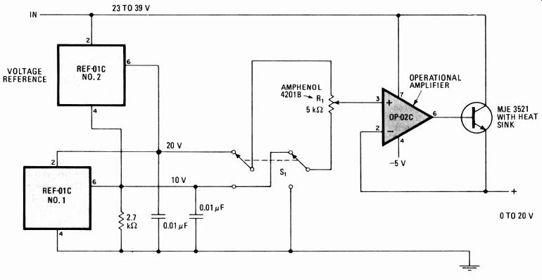
----------- 1. Piggyback. Two series-connected voltage references
may be united to yield an extended supply output range with significantly
improved line regulation at the lower range. The circuit's output can
be set to within 300 µV of the desired value. Maximum output current
is 1 A.
Comparator circuit regulates battery's charging current
By Ajit Pal, Indian Statistical Institute, Calcutta, India
As charge builds up in a battery, its effective plate-charging area gradually decreases. To prevent damage, a good battery charger should continuously limit the charging current from the power line as a function of time. This completely solid-state charger performs the required regulation for a 12-volt automobile battery using a simple circuit built around the µA710 comparator. Although designed for 220-v operation, the charger is easily adapted for 110-v service, making it suitable for application in the U.S.
The comparator automatically adjusts the charging current by sensing the battery voltage, which increases as charge accumulates. The 710 also regulates the current by controlling the on-off switching times of a thyristor that is placed in series with the battery.
As shown in the figure, a dc voltage proportional to the battery voltage is applied to pin 3 of the comparator, with potentiometer R1 determining the actual value.
Simultaneously, a ramp signal that is derived from the power line is fed to pin 2 of the 710, with R2 setting the slope of the ramp.
When the battery is being discharged, the voltage at pin 3 of the 710 is nearly equal to the lowest instantaneous ramp voltage, and so the output of the 710 is virtually always high. Thus, the thyristor is on for almost the entire 180° switching cycle.
At the other extreme, when the battery is almost fully charged, the voltage at pin 3 is practically equal to the highest instantaneous ramp voltage, and so the thyristor is on for only a small portion of the cycle. For intermediate conditions, the thyristor will be on from between 0° and 180° of the cycle. The maximum charging current is limited by the resistor R3.
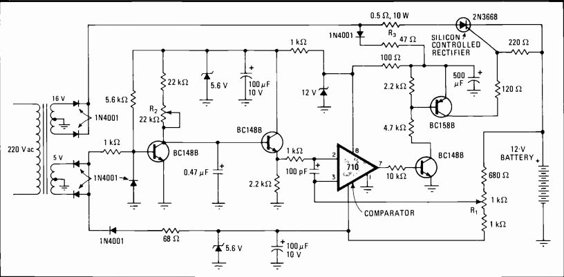
----------- Cutting down. This circuit progressively limits the amount of charging current through a standard 12-V automobile battery as it attains its nominal terminal voltage from its discharged condition, thus avoiding cell damage. The single 710 comparator performs comparison regulation functions. Other circuitry sets conditions where the thyristor can be fired over a 0° to 180° cycle.
[source: ISBN 0-07-606808-0 Copyright 1982 by McGraw-Hill, Inc. ]