One-chip DVM displays two-input logarithmic ratio
by David Watson; Intersil Inc., Reading, Berks., England
The popular ICL7106 series of analog-to-digital converters that serve so widely nowadays as one-chip digital voltmeters can be easily converted to display the logarithm of the ratio between two input voltages, making them useful for chemical densitometry, colorimetry, and audio-level measurements. Only slight wiring modifications at the device's input and integrating ports are required.
Shown in (a) is the new configuration. The modifications from the standard a/d converter connection include the addition of a resistive divider, R1-R2, at the reference inputs, and the placing of resistor R_P in parallel with the device's integrating capacitor.
As shown with the aid of the timing diagram in (b), the time constant of the integrating network is given by Tau = Cint Rp, with the asymptotic endpoint voltage of the integration voltage being Vas = RP (V,- V2)/R,as, where V1 and V2 are the input voltages to be measured. The final integrator voltage therefore becomes Kat = R, (V1- V2)(1 – e^T/r)/R_int, where T is the fixed integration period.
During the de-integration portion of the cycle, the exponential decay moves toward the total voltage, Vtot, which equals Vint + Vref (Rp/Rint). But Vref = kV2, where k is set by the resistive divider, so that Vs., = R_P (V1- V2)(1-e^-T/tau)/Rint + Rp k V2 / Rint . The integrator voltage actually crosses zero when the exponential wave form reaches Vfinal = Vref Rp /Rint = R_P kV2/Rint.
As seen, the time needed to reach the zero crossing is given by TDEINT = rIn(Vias/V final, 1 Making k = (1-e-T") and r = T/2.3, it is realized that TDEINT = T logio( V1/V2). For this condition, k = 0.9, which is achieved by making R1 = 1 MO and R2 = 9 MO.
Theoretically, the system's full-scale output voltage is reached when log 10( V1/V2) = 2, but noise will probably limit the range of the converter. Note also that the accuracy of the system is no longer independent of passive component variations. The simplest way to ensure that k = 0.9 is to use a pre-trimmed divider. The system is calibrated by making V1 = 10V2 and by adjusting R_P until the display reads 1.000.
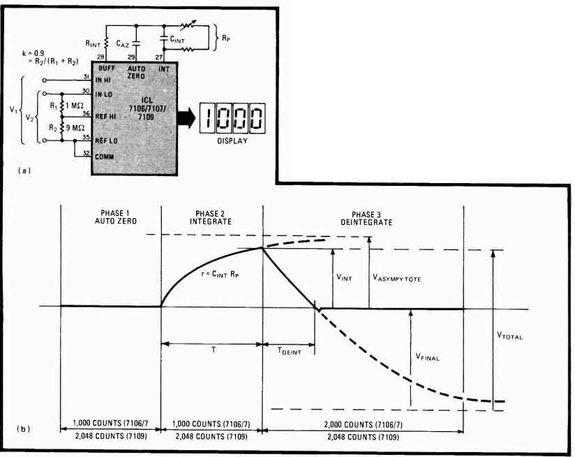
--------- Log converter. ICL7 106 analog-to-digital converter may
be used to measure the logarithmic ratio of two input voltages. Modifying
converter's input circuit (a) and integrating network and selecting suit
able time constants ensure that its output is proportional to log,o(V,/V2).
Timing diagram (b) clarifies circuit operation.
Serial-to-parallel converter decodes width-modulated BCD
by William D. Kraengel Jr., Valley Stream, N. Y
Converting a binary-coded-decimal pulse train into its parallel equivalent is normally straightforward, unless of course, the signal assumes the form of a pulse-width-, pulse-code-, or pulse-position-modulated data stream.
In data-processing cases where the stream is encoded by means of pulse-width modulation, however, this simple 4-bit decoder will serve well in performing the serial-to-parallel transformation.
The MC14538 one-shot, A1, and the CD4015 4-bit shift register, A4, form the central part of the decoder, serving as the timing and storage elements. As can be seen from the schematic and the timing diagram, the BCD input data is grouped into 5-bit cycles, with bit 5 being the framing pulse. A1 must generate a pulse width of tps., = RC = 1/2(t + t2) when triggered, and one-shot A2 has a very small triggering time of t, = R1C1 = 10 microseconds, where both times are defined as shown in the timing diagram.
The firing time for A1 must be selected to correspond to the input frequency of the serial BCD data. Under this condition, the one-shot is triggered by the negative edge of each serial input data bit, and if the serial input data line is low at the time the one-shot times out, a logic 0 is introduced into the shift register. On the other hand, a logic 1 will be read into the shift register if the input data goes high by the time AI times out.
Shift register A3 serves as a counter, acting to disable A4 and enable quad latch A5 and one-shot A2 during the framing pulse. The valid data from A4 (which is inverted) is latched into A5 as AI times out during the framing pulse. Simultaneously, A2 is triggered so as to generate a data available/reset strobe signal for any peripheral control circuitry. The parallel equivalent BCD data and its inverse are available at the outputs of quad latch A5.
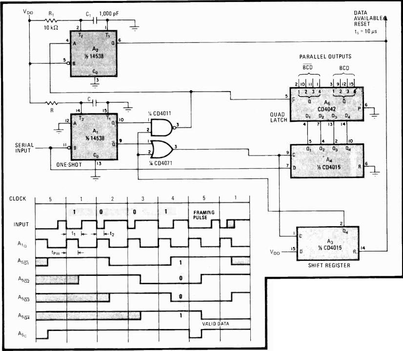
------------ Conversion. Serial BCD data encoded
in pulse-width-modulated form is converted into its parallel equivalent
with this simple decoder. Data-synchronous one-shot A, clocks in serial
input to A., where it is stepped into output latch A5. A2 and A3 handle
framing pulse to coordinate system timing. Timing diagram details circuit
operation.
Switched V-f converter linearizes analog multiplier
by Kamil Kraus Rokycany, Czechoslovakia
This analog voltage multiplier provides a degree of linearity not attainable with circuits that use rudimentary voltage-to-frequency converters. And when modified, it is a more versatile analog divider than the circuit pro posed by Kumar', which finds the quotient for only one fixed reference voltage because of the way its current source is configured. The much improved performance is achieved with a one-chip unit designed specifically for V-f conversion duties, and a simple but accurate switched-capacitor arrangement to do the actual multiplication.
The product of two voltages is found by utilizing the TL604 single-pole, double-throw switches, thereby sampling input voltage V2 periodically and placing a corresponding charge on capacitor C1. The average current that flows to charge Cu during these intervals will thus be proportional to V2, C1, and the sampling frequency, which is a function of input V1. The equivalent resistance corresponding to the average current that flows will therefore be R, = k/C.f, where k is a constant and f is the sampling frequency. Assuming a high sampling frequency, a pure resistance equal to R, may be considered to be in series between the output of the switch and the inverting input of the TL071 operational amplifier, as shown.
Thus the output voltage V., may be expressed as some function of V2 multiplied by the switching function, or, more clearly, as V., =- V2(R2/R) =- V2R2C.f/k, where the sampling frequency, on the order of 50 to 500 kHz for 0 < Vi< 25 v, is generated by the V-f converter.
But the sampling frequency is given by f = V,/2R,Ck,, and so V., = V IV2R2C./RICkki, which is proportional to- V1V2 (constant kl is introduced by the vco).
If the output circuit is modified slightly (see inset), the circuit will function as a divider. Then, V.., =
V2(R/R2) = R2V2k/C.RI C1ki-- V2/ V1. El
References:
1. Umesh Kumar, "Improved analog divider finds large-signal quotients," Electronics, Dec. 6, 1979, p. 135.
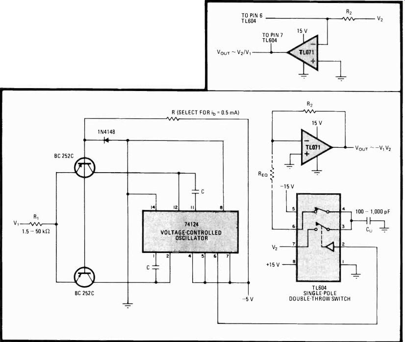
---------- Mathematics. One-chip V-f converter and
switched capacitor arrangement provided by solid-state switches yield
excellent linearity and wide-range voltage-handling performance in an
analog multiplier. Interchanging Re, and R2 by modifying output circuit
slightly (see inset), where Re, represents the average current flowing
in capacitor Cu during sampling period, converts unit into two-input
analog divider.
Voltage-detector chip simplifies V-f converter
by Lloyd Powell David Taylor Naval Ship Research and Development Center, Annapolis, Md.
One-chip voltage detectors such as Intersil's ICL8212 contain all the necessary reference, discharge, and hysteresis circuitry needed to build a simple voltage-to frequency converter. Providing a 0-to-1-kilohertz output for a 0-to-2-volt input in its basic range, the low-cost circuit requires only a few additional passive components, including an operational amplifier.
As shown, A1 integrates incoming signals until its output voltage, and hence also the voltage across capacitor C1, becomes V' rer = Vrer(12.2+ R4)/R2, where Vrd is the internal reference voltage of the ICL8212. At that instant, A2's comparator goes high and switches its output transistor. While transistor Q1 provides a positive going output pulse, C2 holds A2's comparator high, so that C1 is discharged quickly, in just 5 microseconds.
Thus the process of integration and discharge occurs at a rate given by output frequency f = V'in/Vref R1C1.
Linearity and offset are better than 0.2% over the 0-to-1 kHz voltage-to-frequency range, assuming the operational amplifier used has low offset voltage and bias current. Suggested capacitance values for other frequency segments are given in the box in the figure.
The input-voltage range can also be selected by means of R1. For greatest accuracy, capacitors having the highest stability should be selected, and thus those of the silver mica and polycarbonate type should be used where practical. For less stringent applications, those of the ceramic and disk type will suffice.
Supply voltages may range from ± 2 to ± 18 v with out loss of circuit linearity.
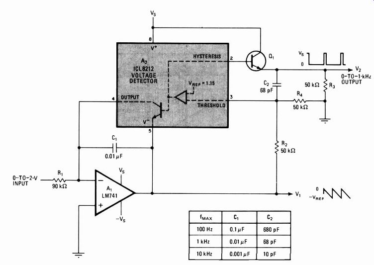
--------- Cost-effective conversion. Micropower voltage
detector chip and op amp form integrating V-f converter. Simple, low-cost
circuit has 0.2% linearity over 0-to-2-volt input range. Frequency range,
nominally 0 to 1 kilohertz, is chosen by appropriate selection of C1 and
C2 (see box).
Low-power f-V converter turns portable tachometer
by Dan Watson Intersil Inc., Cupertino, Calif.
Placing a frequency-to-voltage converter in the form of a complementary-mos timer and operational amplifier at the front end of an analog-to-digital converter reduces the power, wiring complexity, and costs associated with designing an efficient digital tachometer or anemometer for field use. When combined with the multifunctional capability of such a-d converters as Intersil's ICL7106, a direct or scaled reading of the input parameter expressed in revolutions per minute can be readily determined with few additional parts.
The ICL7106 contains not only all of the required clock and display-driving circuitry, but also a reference, so that the external reference voltage normally required in circuits of this type can be omitted.
Signals applied by a magnetic or optical transducer to the input of the ICM7555 timer (powered by the converter's reference voltage) are converted into fixed-width pulses of corresponding frequencies. The ICL7611 micropower op amp integrates these pulses, and consequently the smoothed signal introduced to the a-d converter is a direct function of the input frequency. Thus, the signal will have an amplitude of Vin = (RPM/60)(t,,,,)(Vr)(E)(R4/R3) where tpy, = pulse width of timer = 1.1 R2C2 Vr = reference voltage of ICL7106 = 2.8 volts E = number of events per revolution from the mag netic or optical sensor, the number of fan or propeller blades, or the number of point closures per revolution in an automotive application.
The converter's full-scale output is 200 millivolts.
Note that the V timer port is powered by the internal low-reference voltage of the converter, precluding the need for a second reference because of the rail-to-rail output swing of the ICM7555.
The output of the converter is given by n = ( V1riVr) (R2+ R8)/R8a. The a-d converter contains on-chip display circuitry for driving a liquid-crystal display. If a light-emitting-diode display is desired, the a-d converter can be replaced with its sister unit, the ICL7107.
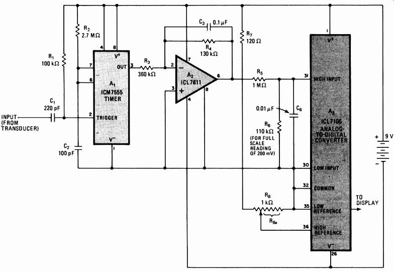
-------- Restless wind. Complementary-MOS chips combine to make a
simple, cost-effective flea-powered digital tachometer or anemometer
for field use. Input signals of corresponding frequency from magnetic
or optical transducers are converted into voltages by A, and A2, and
then into the equivalent digital output by A3. R3-1={4, and IR7-F16 set
the scaling multipliers.
Integrator improves 555 pulse-width modulator
by Larry Korba Ottawa, Ont., Canada
In one method of providing linear pulse-width modulation with the 555 timer, a current source charges a timing capacitor, creating a ramp signal that drives the modulation input of the 555. Unfortunately, the circuit offers only a limited dynamic range of pulse widths and is highly sensitive to temperature. A better way is to use a resettable integrator as the timing element.
Charging with a constant current source (a) at best yields a 2:1 dynamic range for a supply of 5 volts-the linear operating range for voltage-to-pulse-width con version is approximately 2.1 to 4.1 v, and the timing capacitor is totally discharged every timing cycle. Furthermore, the circuit requires temperature compensation to eliminate any timing fluctuation due to the tempera ture sensitivity of Q1, since the base-emitter voltage varies at the relatively high rate of-5 millivolts per °C.
And, to add to the circuit's woes, Lb° varies with temperature as well.
The resettable integrator (b) made up of A2, Q1, C, and R applies a trigger pulse to the 555, causing QI to turn off. Integrator A2 then ramps up until the voltage level at the modulation input of the timer equals that at pin 5. When that happens, Q1 is turned on again, reset ting the integrator and turning off the 555.
The voltage applied to the integrator, V is set to 2.1 v. This makes the shortest linearly modulated pulse width equal to the trigger pulse width-2 microseconds.
With the timing values shown, the maximum pulse width is 6 milliseconds, producing a dynamic range of more than 3,000:1 over the linear operating region.
The active components affecting the timing circuit are A2, Q1, A1, and V, Since the average temperature coefficient for the offset voltage of A2 is a very low 5 microvolts/°C (affecting the timing by only 2.5 parts per million/°C), the circuit's almost negligible adverse temperature effects are largely due to the variation with temperature of the off current of Q1, Id.. Id. doubles every 10°C; for the 2N4360, it is about 10 nano-amperes at room temperature.
It is important to note that for both circuits, the effects of Vc, and the 555 on timing stability are the same. As a bonus, however, the new circuit provides a linear ramp output that can be loaded fairly heavily without seriously affecting circuit timing.
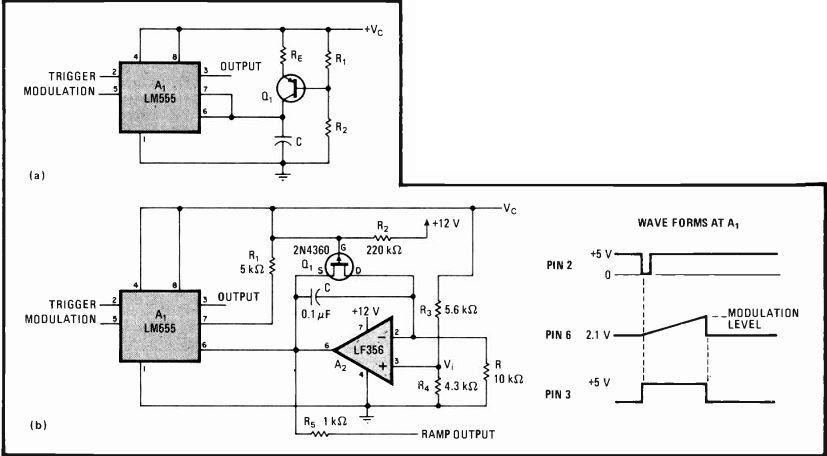
------------ Old style, new style. In the most common method of linear
pulse-
555 timer integrated circuit (a), the timing elements are current source Q, and capacitor C. The sensitivity of the pulse characteristics to circuit parameters leaves much to be desired.
When a resettable integrator is used to time the modulator (b), circuit sensitivities are reduced greatly. As a bonus, pin 6 provides a ramp output with significant drive capability.
Dithering' display expands bar graph's resolution
by Robert A. Pease National Semiconductor Corp., Santa Clara, Calif.
Commercially available bar-graph chips such as National's LM3914 offer an inexpensive and generally attractive way of discerning 10 levels of signal. If 20, 30 or more steps of resolution are required, however, bar-graph displays must be stacked, and with that, the circuit's power drain, cost and complexity all rise. But the techniques used here for creating a scanning-type "dithering" or modulated display will expand the resolution to 20 levels with only one 3914 or, alternatively, make it possible to implement fine-tuning control so that performance approaching infinite resolution can be achieved.
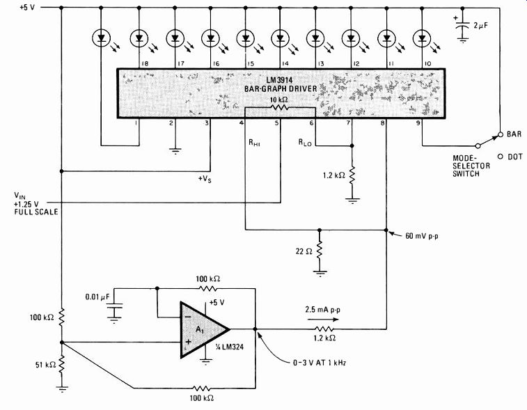
----------- 1. Half tones. Input-signal biasing on LM3914 bar-graph
chip is set by the instantaneous output of a low-amplitude square-wave
oscillator so that bar-graph resolution can be doubled. Each of 10 LEDs
now has a fully-on and a partially-on mode, making 20 states discernible.
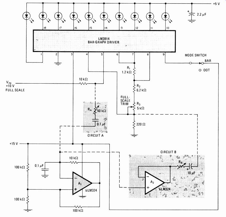
-------------- 2. Spectrum. Greater resolution, limited only by the
ability of the user to discern relative brightness, is achieved by employing
a triangular-wave oscillator and more sensitive control circuitry to
set the voltage levels and thus light levels of corresponding LEDs. Two
RC networks, circuits A and B, provide required oscillator coupling and
attenuation. B replaces A if oscillator cannot suffer heavy loading.
The light-emitting-diode display arrangement for simply distinguishing 20 levels is achieved with a rudimentary square-wave oscillator, as shown in Fig. 1. Here, the LM324 oscillator, running at 1 kilohertz, drives a 60-millivolt peak-to-peak signal into pin 8 of the 3914.
Now, the internal reference circuitry of the 3914 acts to force pin 7 to be 1.26 v above pin 8, so that pins 4 and 8 are at an instantaneous potential of 4.0 my plus a 60-mv p-p square wave, while pins 6 and 7 will be at 1.264 v plus a 60-mv p-p square wave. Normally, the first LED at pin 1 would turn on when V,n exceeded 130 my, but because of the dither caused by the ac component of the oscillator's output, the first LED now turns on at half intensity when V, rises above the aforementioned value. Full intensity is achieved when V, = 190 my.
When rises another 70 my or so, the first LED will fall off to half brightness and the second one will begin to glow. When V, reaches 320 my, the first LED will go off, and the second will turn on fully, and so on. Thus 20 levels of brightness are easily obtained.
Similarly, greater resolution can be achieved by employing a triangular-wave oscillator and two simple RC networks as seen in Fig. 2. Here, by means of circuit A, this voltage is capacitively coupled, attenuated, and superimposed on the input voltage at pin 5 of the LM3914. With appropriate setting of the 50-kilohm potentiometer, each incremental change in V, can be detected because the glow from each LED can be made to spread gradually from one device to the next.
Of course, if the signal-source impedance is not low or linear, the ac signals coupled into the input circuit can cause false readings at the output. In this case, the circuit in block B should be used to buffer the output of the triangular-wave oscillator.
The display is most effective in the dot mode, where supply voltages can be brought up to 15 v. If the circuit's bar mode is used, the potentials applied to the LEDs should be made no greater than 5 v to avoid overheating.
To trim the circuit, set the LM3914's output to full scale with R3. RA or RB should then be trimmed so that when one LED is lit, any small measured change of V,. will cause one of the adjacent LEDs in the chain to turn on.
Multiplexers compress data for logarithmic conversion
by Andrzej Piasecki Warsaw, Poland
Cascaded multiplexers and a few gates are all that is needed to build this digital log converter, which compresses an 8-bit signal into a 5-bit number according to the transformation 2^n ---> 4n. Conversion to higher numbers is achieved by cascading additional multiplexers and appropriate gating circuitry.
As seen in the figure and the truth table for n extending from 0 to 28, the design of the circuit is simplified because each of the circuit's 74157 multiplexers can transfer without alteration 4 bits of the signal formed by a preceding multiplexer.
Alternatively, following multiplexing it can transport input bits that extend the second and third digits to the two least significant bits at the output.
As a result, the two most significant output bits of any multiplexer are fixed within a given input-number range.
They are encoded by transferring the given 0 and 1 logic states into successive multiplexer inputs, with the most significant input bit (at logic 1) switching on whichever multiplexer is appropriate for transferring the desired number to the output.
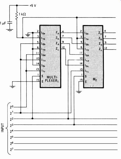
------- Multiplexer manipulation. Using digital multiplexers, this
circuit converts 8-bit input numbers into their corresponding 5-bit logarithmic
equivalents, performing the operation in 100 ns. The truth table illustrates
the simplicity of the design technique that performs the conversion.
Multiplexers may be cascaded for extending the range over which n may
be transformed into its log value.
As the input number decreases, the number of multiplexers required to transfer the desired data increases. NAND gates G1 through G5 derive the logic value of the most significant bit of the 5-bit number at the output. Note that the algorithm used will necessitate that the designer observe considerable care in wiring up the additional multiplexers that would be required to process larger numbers.
The propagation time of a digital logarithmic conversion is about 100 nanoseconds. The circuit draws no more than 120 milliamperes.
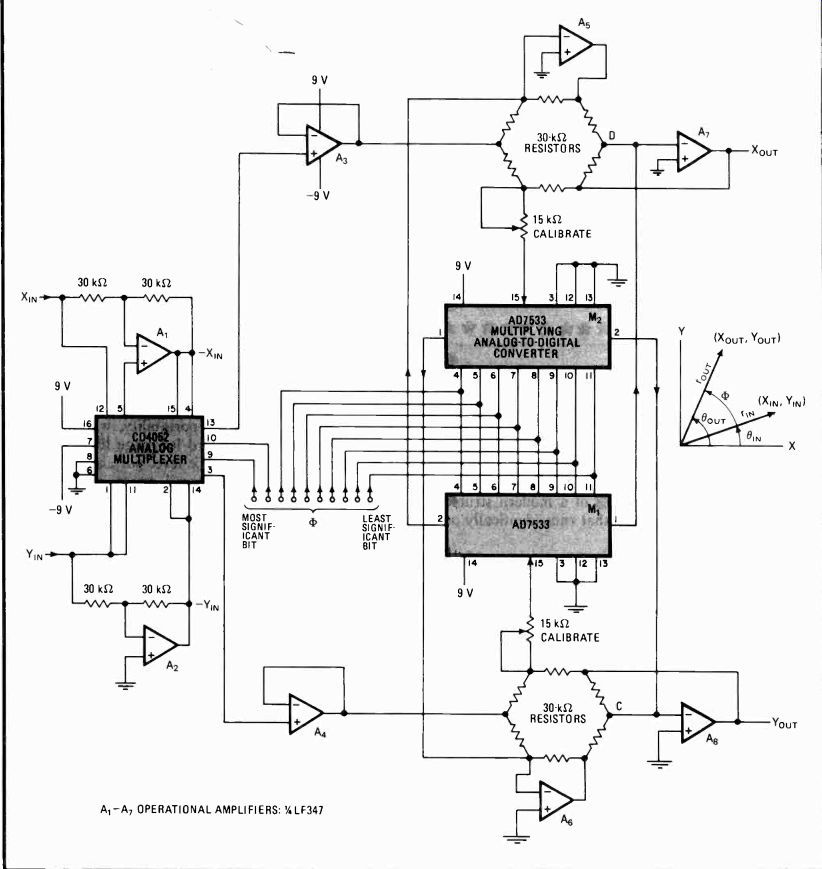
Low-cost coordinate converter rotates vectors easily
by Arthur Mayer
Sperry Systems Management, Great Neck, N. Y.
Especially useful for graphics display applications, this simple $15 vector rotator, which takes coordinates in the x-y Cartesian system and adds an angle of rotation to produce new coordinates x', y', is faster and cheaper than others currently available.
--------- Transformation. Input data for positioning a cursor in
graphic displays, often presented in x-y (Cartesian) coordinates, may
be rotated by 4' in steps of 0.35° to new location x', y'. One analog
multiplexer, two multiplying d-a converters and eight op amps in a unique
cross-fed summing network perform the operation. Alternatively, the circuit
will transform a vector from polar (r,O) into rectangular (x,y) form.
As shown in the schematic, the analog voltage pair (x,y) represents the vector ra, where r2 = x' + y' and tangent 0 = y/x. The two inputs xiN, yiN-together with- xiN,- yIN obtained from inverting amplifiers A1 and A2-are applied to the CD4052 dual analog multiplexer, which is controlled by the two most significant bits of the binary-coded rotation angle phi. Each dual multiplexer output signal passes through a unity-gain amplifier, A3 or A4, and then through a tandem of inverting amplifiers (A5, A7 or A6, A8) to the final output.
Each tandem of inverting amplifiers is coupled with an AD7533 multiplying digital-to-analog converter to make a four-quadrant multiplier: A5 and A7 are coupled with M1 , and A6 and A8 are coupled with M2. The digital input to both converters is provided by the remaining bits of phi.
The analog input to M1 is the average of the signals from A4 and As, and the analog input to M2 is the average of the signals from A3 and A7. The output currents from the cross-fed d-a converters feed the summing junctions of As through A8, where they add to the inputs that have been selected by the multiplexer, thus producing the output voltages ROUT, YOUT.
All resistances in the circuit are 30 kilohms so it is convenient to use dual in-line packages, like Beckman's 698-3, with eight resistors per DIP. Another DIP, Bourns's 7102, could replace the two 15-kf2 trimmers needed to raise the effective input impedance of each AD7533 to 15(2)1/2 kS1, the value required in this design.
Regardless of the value of phi, x2ou-r+ y2ouT = x2IN + y2IN.
In other words, the output vector's magnitude is always equal to that of the input vector. However, the relationship between the input and output vectors is given by Owl' = BIN + (1,/, where tan(472) is equal to (2 1/2- 1)( phi-45°)/45° and phi is between 0° and 90°. The difference between 4' and 4.- 45° vanishes for 4 = 0°, 45°, and 90° and is always less than 1° for other values of phi in the first quadrant. Note that the error and its variation with angle recur in the other three quadrants.
The 45° offset in 4' is due to the bipolar operation of the AD7533 converter. The offset may be corrected by simply adding 45° to the digital equivalent number at the phi input lines. The remaining error will be small enough to go unnoticed on most graphical displays.
To calibrate the vector rotator, xIN is set to some constant voltage and set yiN = 0. Then the trimmers are adjusted to make xour + Your = 0 when phi = 0° and ROUT- yOUT = 0 when phi = 90°.
With the addition of a clock and a counter to make phi = wt, the vector rotator becomes a sine-cosine generator.
For example, for a 5-volt root-mean-square output, xiN and YIN is set to 5 v dc; then ROUT = 5(2)1/2 cos wt and YOUT = 5(2)1/4 sin wt.
Because of the functional error in the angle as given by the formula for tan(472), either output will contain third and fifth harmonics each having a magnitude 0.8% that of the fundamental. Total harmonic distortion, therefore, is 1.1%.
Adapting a home computer for data acquisition
by Peter Bradshaw Inters'', Inc., Cupertino, Calif.
A personal computer, of the kind made by Apple and Atari, can be easily interfaced with an instrumentation module if a machine interrupt is used to overcome their inherent incompatibility--a condition attributable to the different clock speeds at which module and machine run.
The interrupt scheme shown here facilitates the transfer of data by exploiting the data-ready signal available on most modules that generate a multiplexed binary-coded decimal output. Thus, the computer can be freed for other tasks, as in any timeshared system.
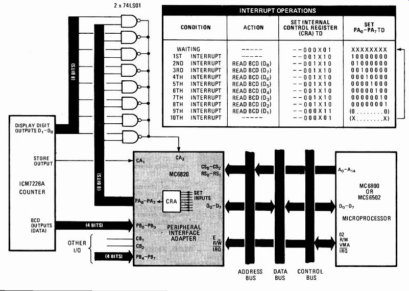
-------- Prompt servicing. Using an interrupt scheme,
instrumentation modules and other data-gathering processors with BCD multiplexed
outputs can be readily interfaced with home computers such as the Apple
and the Atari. Interrupts for reading the data corresponding to each display
digit of counter in succession are generated by the microprocessor system
itself, which produces a pulse at CA2 each time the contents of its updated
Pk-PA, output register equal that of the scanned display digit outputs
D1-D8.
As an example, consider the arrangement in the figure whereby the Intersil 7226 multipurpose counter is inter faced with the popular MC6800 or MCS6502 microprocessors, which are at the heart of many personal computing systems. After the counter measures a designated interval, its store output moves low, signaling the MC6820 peripheral interface adapter with an interrupt request. This interrupt should be serviced within 100 milliseconds and control register CRA and the ports PA0-PA, set to the required bits (see table).
Thereafter, an interrupt is generated through the PIA's CA2 port and the 74LS02 open-collector NAND gates each time the multiplexed display-digit outputs of the counter match that of the bits on the PA0-PA7 lines. The BCD output data corresponding to each display digit D1-D0 is thus successively applied to the P130-PB3 inputs (at a 4-kilohertz rate) and then to the processor.
The second through ninth interrupts should each be typically serviced in less than 244 microseconds. This task can be easily accomplished if proper priority is assigned to the interrupts. Thus the data will be read in less than 4 ms, so there will be no problem with data overruns (200 ms between measurements).
Ideally, the first interrupt should either include a check to ensure that digit D8 is not high and the input is correct or else be followed by a statement that creates an interrupt when line D1 is high. In addition, the computer bus will usually require some form of bidirectional buff ering to the peripheral interface adapter.
The same system can be used with any processor in the MC6800 series; with other processors, a morecom plex interrupt-handling scheme is required.
[source: ISBN 0-07-606808-0]