FSK transmitter uses two gated oscillators
by Akavia Kaniel Meesurex Corp., Cupertino, Calif.
The 4528B complementary-mos dual monostable multi-vibrator can operate as a frequency-shift-keyed (FSK) transmitter. Each half of the chip, shown in Fig. 1, is used here as a gated oscillator and is activated either when a mark or a space frequency is to be transmitted.
As long as the input signal to the clear input (CLR pin 3) is present, transistor Q1 is turned on and the oscillator will not oscillate. Once the CLR pin is pulled high, however, Q, turns off and the outputs of flip-flops No. 1 and 2 turn low. Transistor Q2 turns on for an instant, triggering the self-starting oscillator. At the same time flip-flop No. 1 senses that point A, shown in Fig. 1, has gone low and turns Q2 off.
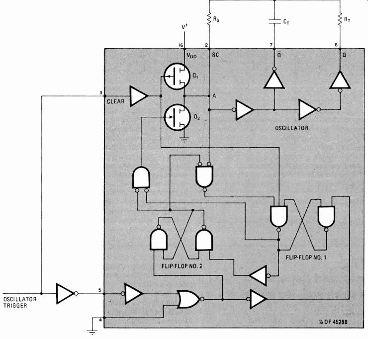
-------------- 1. Shifty. The core of the frequency-shift-keyed transmitter
is a gated oscillator, which is controlled by a signal present at the
clear (CLR) pin.
The full circuit uses two such oscillators-one for a mark and another for a space-contained in a 4528 dual one-shot package.
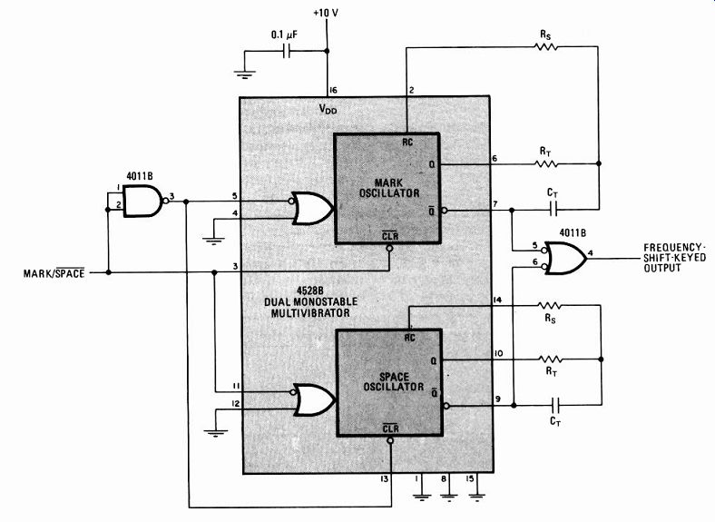
-------------- 2. Coupled. A complete frequency-shift-keyed transmitter
is formed by coupling the outputs from both monostable multivibrators
through a dual-input NAND gate, as shown here. Mark and space frequencies
are fixed by FIT and CT, where Rs = 2RT.
With Q1 and Q2 off, the oscillator runs at a frequency determined by resistor RT and capacitor CT and is given by the expression: F = 1/( 2.3 X RT X CT) for 1 kilohertz F.'S MO kHz, where Rs As 2 x RT.
When the CLR input is pulled low, Q1, turns on and the oscillation stops. The complete FSK transmitter circuit is shown in Fig. 2. It is formed by coupling both oscillator outputs. When the mark-to-space control input goes high, the mark oscillator signal appears at the FSK output, and when the same line is low, the space oscillator signal appears at the FSK output.
Simple sound generator takes orders from microcomputer
by Joseph Huijts Waalre, the Netherlands
Only six integrated circuits are required to build this low-cost programmable sound generator. The circuit, as shown in the figure, permits a choice of 8 different levels of loudness, 16 time durations, and 8 frequencies (they are not related to musical intervals).
In operation, 2 bytes of data are sent from a micro computer to this circuit, which produces a tone. The duration is programmable; thus no action from the microcomputer is required to end the tone.
The first byte is sent to a 40174 hex D-type flip-flop, to control frequency and loudness. The second byte is sent to a 4029 binary/decade counter with the ability to load data in parallel. The least significant nibble is loaded into the counter enabling an oscillator circuit-a NAND Schmitt trigger with RC feedback. This oscillator causes the counter to decrement until it is inhibited by the final count indicated by the CARRY OUT pin going to a logic 0. The time span that is produced depends on both the oscillator frequency (about 10 hertz) and the nibble that is loaded into the counter. In this way 16 different time spans can be selected from 0 to 1.5 seconds in 0.1 second steps.
The final count output also controls a second oscillator, producing the output tone. The frequency is con trolled by the R and C values of the feedback circuit.
The capacitor can be paralleled by a programmable combination of other capacitors with three bilateral analog switches like those used in a 4066, set by the most significant nibble of the 40174 hex dual flip-flop. The frequency can be adjusted between 700 and 2,300 Hz.
The least significant nibble controls the loudness in eight 5-dB steps with a 74LS145 binary-coded-decimal-to-decimal decoder-driver. The sound-producing frequency is connected to the D input of the 74LS145, selecting outputs 0-7 when low or outputs 8 and 9 (not connected) when high. The A, B and C inputs-controlled by the least significant nibble-select a resistor to feed the loudspeaker. A 2-microfarad tantalum capacitor rounds the edges of the generated square wave.
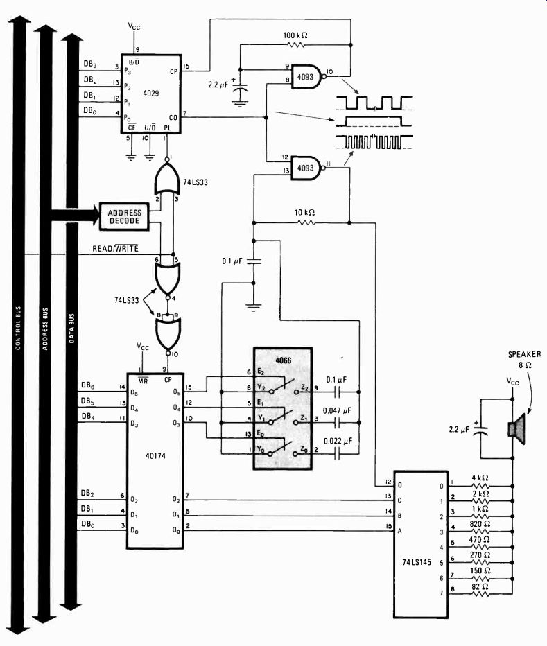
-------------- Sound off. Programmable sound generation under microcomputer
control is achieved by decoding information on the address bus This decoding
directs frequency and loudness information bytes to the 40174 hex flip-flop
and duration information bytes into the 4029 counter.
Op-amp summer forms simple high-speed phase generator
by Dieter R. Lohrmann Department of the Army, Harry Diamond Laboratories, Adelphi, Md.
A simple operational-amplifier summing circuit can generate an output voltage that is a rectangular- or sine-wave function of a dc source potential. For analog applications such as the direct phase modulation of a radio-frequency carrier, this circuit combines fast response with low throughput delay, making it superior to the often-used method of digitizing and reconverting an input signal with the aid of a microprocessor. In digital uses it can generate a pulse train having almost any pulse voltage-versus-dc input voltage characteristic.
In the circuit's general configuration, which for simplicity omits the stabilizing circuitry like bypass resistors and capacitors, resistors R1-R7 form a voltage divider whose taps are alternately connected to the inverting and noninverting inputs of the adjacent comparators A1-A6.
The outputs of the comparators are simply summed via resistors R8-R13.
For a digital application (a), the incoming ramp is used to generate a variable pulse-width train. When the ramp voltage is below the node voltage at point 1, comparators A1, A3, and A5 are low (-7 volts), whereas A2, A4, and A6 are high ( + 7 v). Thus, the output voltage will be midway between the two supply voltages, or at zero.
As the ramp rises above the node voltage at point 1, comparator A1 switches, activating a fourth comparator, while two remain off. The output voltage thus jumps to 2 v, assuming resistances R8 to R13 are of equal value. This voltage remains constant while the ramp voltage increases, until it exceeds the potential at the divider's second node, causing comparator A2 to switch off. At this time, A2, A3, and A5 are low, and A1, A4, and A6 are high, returning the output voltage to zero.
As the ramp voltage climbs past the potential at the third node, a similar operation moves the output to 2 v, because four comparators will be on and two will be off.
The output drops to zero again when the ramp moves to a potential higher than at node 4.
The duration of each transition will be dependent upon the node and dc input voltages, which may be appropriately selected by the user. Consequently, a pulse train having almost any set of variable-width characteristics can be ordered.
In analog applications, a good approximation of a sine-wave function can also be generated if the voltage divider's switching intervals are made equal to AV, the voltage increment required to switch the output of each comparator from negative to positive saturation. Because the comparator's transitions are nonlinear, the steep sides rectangular transfer function are rounded off, and therefore a sine wave can be very nearly approximated.
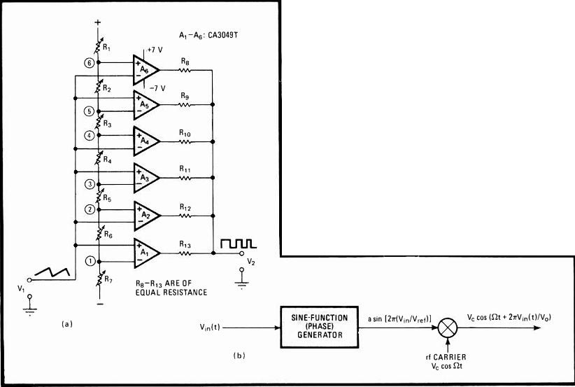
---------- Speedy switching. Op-amp summing stage (a), wired in an
inverting-to-noninverting input arrangement, provides sine- or rectangular-wave
phase generation for fast response and low throughput delay. If the comparators'
thresholds are selected so that the summer's switching profile approximates
a sine wave, the circuit may be used to phase- or frequency-modulate
an rf carrier directly (b).
Such a scheme is useful in phase or frequency modulators, as shown in (b), because it enables direct modulation at any arbitrarily large modulation index without introducing additional frequency offset. The function generator's output is simply introduced at the intermediate-frequency port of a single-sideband modulator. At the output of the modulator will appear the sum of the i-f and rf frequency, which is a cosine function applied to the modulator's rf port.
In this case, the function generator performs a phase modulation, because the phases of the generator and the rf carrier are added in the modulator. Thus, V, causes a phase modulation of the rf carrier. The maximum modulation index is determined by the number of amplifiers in the phase generator. For a maximum modulation index of M, 2M/ir amplifiers are necessary.
If the SSB modulator is of the phasing type (which cancels the lower sideband by phase-shift mixing), orthogonal signals will be required at its i-f and rf ports.
This function generator can be easily modified to generate a cosine-function signal, instead of a sine-wave output. Thus, a sine- and cosine-function generator may be combined to provide the orthogonal signals required for the SSB mixer.
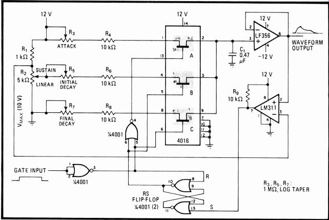
Adjustable ex generator colors synthesizer's sounds
by Randall K. Kirschman Mountain View, Calif
Providing the control signals for voltage-controlled amplifiers, oscillators and filters in order to modulate sound parameters such as loudness, pitch and timbre, this adjustable ex generator is the indispensable ingredient required to attain superior performance in a music synthesizer. Only four integrated circuits and a few passive components are needed in the inexpensive unit, which costs under $6.
When gated or triggered, the generator produces a waveform that passes through four states:
An exponential attack.
An initial decay, or fallback.
A sustain, or steady dc level.
A final decay, or release.
Each of these four parameters is continuously variable, so that waveforms having a large variety of shapes can be generated.
The waveforms are generated by the sequential charging and discharging of capacitor C1 (see figure). In general operation, C1 is connected to a current source or sink as required, through the 4016 complementary-mos analog switches. These switches are controlled by simple logic set into action by the gate-input pulse. Triggered operation is made possible by adding a monostable multivibrator to the circuit.
In the dormant state (gate input low), analog switch C is on, switches A and B are off and the RS flip-flop formed by two 4001 NOR gates is reset. The onset of a gate pulse turns on switch A and turns C off. Consequently, C1 charges through R3 and R4, producing the attack segment of the waveform. Note that the LM356 buffer protects C1 from excessive loading.
When the voltage across C, reaches V.. (determined by voltage divider R1-R2), the LM311 comparator sets the RS flip-flop. This action in turn switches B on and A off. Thus the initial decay segment is generated as C1 discharges through R5 and R6 to reach the sustain voltage, the level of which is determined by the setting of potentiometer R2.
Concurrently, the comparator's output has gone low, but the RS flip-flop remains set until the gate pulse moves to logic 0, at which time switch C turns on. Thus C1 discharges through R7 and R8 to produce the final-decay portion of the wave, after which the circuit reverts to its dormant state.
-----------168
Musical tint. Four-state generator provides myriad control waveforms
for modulating voltage-controlled amplifiers, oscillators, and filters
In a music synthesizer, and thus is useful for coloring loudness, pitch,
and timbre. Attack and decay times are variable from 5 to 500 milliseconds;
sustain level is adjustable from 0 to 10 volts.
Two-chip generator shapes synthesizer's sounds
by Jonathan Jacky Seattle, Wash
Generating the same adjustable modulating waveforms for a music synthesizer as the circuit proposed by Kirschman', but using only two integrated circuits, this generator also works from a single supply. It has, in addition, separate gate and trigger inputs for providing a more realistic keyboard response.
When gated or triggered, the generator, which is built around Intersil Inc.'s C-MOS 7555 timer, produces a waveform that passes through four states:
An exponential attack.
An initial decay, or fallback.
A sustain, or steady de level.
A final decay, or release.
Each of these four parameters is continuously variable, so that waveforms having a wide variety of shapes can be generated.
The waveforms are generated by the sequential charging and discharging of capacitor C1. Here, the 7555 controls the sequencing while diodes switch the currents, unlike Kirschman's circuit where comparators and flip flops control the stepping and analog switches steer the currents. Furthermore, the 7555 is well suited for handling the two logic signals provided by most synthesizer keyboards-the gate, which is high as long as any key is depressed, and the trigger, which provides a negative pulse as each key is struck. The gate and trigger features eliminate the need to release each key before striking the next to initiate an attack phase.
In the dormant state (the gate input at pin 4 of the 7555 is low), capacitor C2 is discharged. When the gate goes high and a trigger pulse appears at pin 2, the 7555 output (pin 3) goes high and charges C1 through R3, R4, and D1, producing the attack segment of the waveform.
Note that diode D2 is reverse-biased because pin 7 of the 7555 is high and that diode D3 is back-biased by logic 1 signal applied to the gate input.
When the voltage across C1 reaches 10 volts, pin 3 of the 7555 goes low and pin 7 is grounded, terminating the attack phase. D1 and D3 are now reverse-biased and C1 discharges through D2, R5, and R6 to produce the initial decay. The sustain level reached is determined by the voltage divider formed by resistor R1 and potentiometer R2. During this phase, a second attack can be obtained by striking another key (see timing diagram). When the last key is released, the gate goes low and C1 will discharge through D3, R7, and R8 to produce the final decay. The CA3130 operational amplifier serves as a buffer to protect C1 from excessive loading.
References:
1. Randall K. Kirschman, "Adjustable e' generator colors synthesizer's sounds," Electronics, July 17, 1980, p. 123.
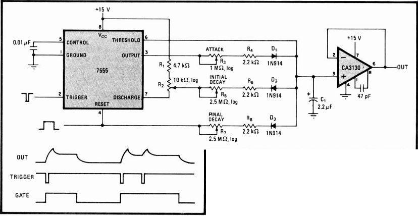
--- In tune. Four-state generator provides control
waveforms for modulating voltage-controlled amplifiers, oscillators,
and filters in a music synthesizer and thus is useful for coloring loudness,
timbre, and pitch. Circuit can be retriggered during its decay/sustain
phases. Attack time is variable from 5 milliseconds to 2 seconds. Initial
and final decay times can range from 5 ms to 5 s. The sustain level has
a dynamic range of 0 to 10 V.
Sync clock, counter improve programmable-width generator
by M. V. Subba Rao and V. L. Path Central Electronics Engineering Research Institute, Pilani, India
The typical programmable pulse-width generator either has limited programming capability or creates an initial timing error because of the asynchronism between an input trigger and the system's internal clock. Employing a binary-coded-decimal-programmable divide-by-n counter and a synchronous-start oscillator in a basic circuit overcomes these drawbacks, as shown here.
A trigger to the B. input of the 74121 monostable multivibrator generates a pulse that presets the 7476 flip-flop and also loads a preset number into the 74192 divide-by-n counter. The flip-flop then initiates pulse generation in the 74123 oscillator, whose output is counted down by the 74192 until zero is reached.
At this time, its borrow output, B3, clears the flip-flop and the oscillator is disabled. The pulse width of the waveform at Q3 is thus proportional to the number of clock pulses counted.
For the component values specified in the figure, the clock period is 1 microsecond. Thus, the circuit will generate pulses of from 1 to 9 As, in steps of 1 The 74192s can be cascaded to yield larger pulse widths.
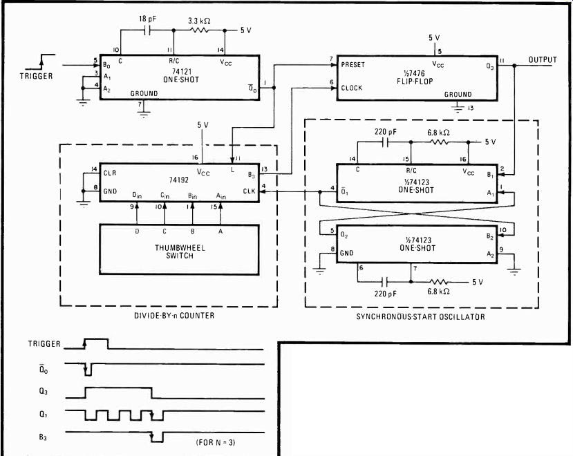
---- Precisely programmable. Divide-by-n counter and synchronous-start
oscillator combine to expand range of pulse-width programmable one-shot
and to eliminate initial timing errors due to asynchronous triggers.
Pulse widths of from 1 to 9µs can be selected, in 1-µs steps. The 74192s
can be cascaded for larger widths.
Four chips generate pseudorandom test data
by Wayne Sward Sperry Univac Division, Salt Lake City, Utah
The inexpensive pseudorandom-bit-sequence generator shown here requires only four integrated circuits and will serve well in testing digital data links. Joined through a minimum of interconnections, it will furnish a recurring 511-bit string suitable for a variety of other applications as well.
The octal D-type latches in A1, along with flip-flop A2, form a 9-bit serial shift register- that drives binary counter A3, which detects the register's illegal all-zero state; exclusive-OR gate G1 provides the required feed back connection. On power-up, the outputs of A1 assume arbitrary logic values, and the 11-megahertz system clock steps the bits to the load input of A3. When the first logic-1 bit cycles through to A3, the counter presets to 6. As long as at least 1 bit in the shift register thereafter contains a logic 1, A3 can never reach a count of 15. Consequently, its terminal-count output will always remain low.
If only zeros should appear in the shift register after power-up or during the course of operation, however, A3 will eventually reach a count of 15, and its terminal count output will go high. This action forces the three-state outputs of A1 to become inactive, or an open circuit, and a logic I will be introduced (through resistor 111) into the data stream, at the D input of A2. This bit is detected by A3 on the following clock cycle and normal operation is restored. Note that the circuit configuration eliminates the nine-input gate that is usually required at the input of the counter in order to detect the existence of an all-zero state.
The test code generated by this circuit is shown in the table, its format being compatible with the popular HP3780 bit-checking data unit. Of course, if the format of the test code must be altered, it may be changed simply by connecting the load input of A3 to the appropriate stage of the shift register.
If the low-power Schottky chips used in this generator are all replaced by their standard Schottky equivalents, the bit rate can be extended to 26 wiz, though with a slight penalty in power dissipation. No additional wiring changes will be required.
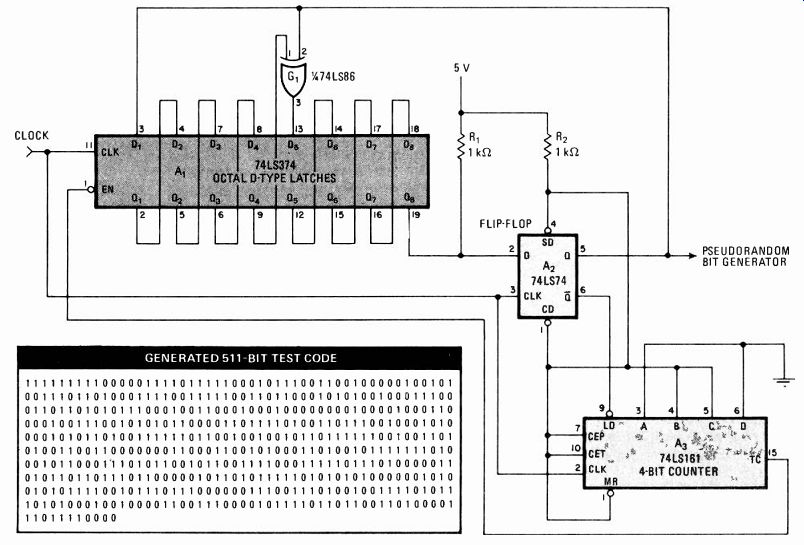
------------ Self-correcting code. Simple generator provides a serial
string of 511 pseudorandom bits suitable for testing digital data links
at up to 11 MHz. The code, in a format compatible with the popular HP3780
test generator or data-bit checker, is easily changed by connecting the
counter to the appropriate stage of shift register A,-A2. Bit rates to
26 MHz are achieved by replacing ICs with their Schottky counterparts.
Two-chip pulse generator operates at 75 MHz
by M. U. Khan Systronics, Naroda, Ahmedabad, India
Built from integrated circuits in the emitter-coupled-logic family, this pulse generator can provide independent control of delay and width (variable from 5 nano seconds to 0.1 second) over the frequency range of 10 hertz to 75 megahertz. Only two chips are required-a quad line receiver and a dual D-type flip-flop.
The MC1692 line receiver, A1a, configured as an astable multivibrator, provides a steady stream of pulses, at a frequency determined by R1 C1, to the delay portion of the circuit. This section, which uses a second line receiver and one half of the MC10231 dual flip-flop, generates a corresponding pulse at the output of Ala whose duration is proportional to R2C2. Its maximum duty cycle is greater than 80% at 10 MHz and decreases progressively to about 50% at 75 MHz. After inversion by Ak, the signal is introduced to flip-flop A2b.
A2b is triggered on the positive-going edge of the signal, and so pin 15 of the flip-flop moves high after a time proportional to R2C2, thus effecting the delay time.
The duration of the pulse emanating from A2b (that is, its width) is set by the A2b-A id combination, which is identical to the A2a-A1b configuration. Note that the polarity of the output appearing at Q2 of A2b matches that of the input signal, because the width-determining one-shot works on an inverted version of that signal.
If the flip-flops are replaced by two MC1670 types, the circuit will work beyond 100 MHz. In either case, the circuits used should be mounted on suitable heat sinks.
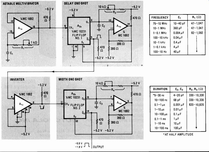
------- Fast and flexible. A simple ECL pulse generator provides
independent control of pulse width and delay and works to 75 MHz. The
tables outline the component values. Operation can be extended to 100
MHz by substituting an MC1670 flip-flop for A2.
Deglitcher-delay circuit serves also as pulse generator
by B. Seastrom and G. Goodwin Sylvania Systems Group, GTE Products Corp., Needham Heights, Mass.
Sustaining its input pulse for a number of clock cycles before translating it into an output pulse, this circuit provides an effective means of discriminating between valid data and spurious pulses or glitches. The designer who uses the circuit has numerous options for adjusting the delay between the input and output transitions, as well as controlling the duration of the output pulse.
Furthermore, it triggers on either a rising or a falling edge and generates complementary outputs.
Data entering serial shift register A1 is sampled at the clock rate and shifted along from output QA to QH.
Meanwhile, for the complement of the input at the output of A2, the same process occurs at the shift register A3. Since all is are required at gates A4 or A5 to toggle cross-coupled NAND gates A6 and A7, there is a delay in the leading edge of the output, as well as in the pulse duration. The delay and the pulse duration depend on how many and which taps are connected from the shift registers to the eight-input NAND gates.
It is apparent that noise-in fact, any changes in input level--will be subject to successive samples, whose number is equal to the tap count, before it results in a change in output. By employing different numbers of taps on registers AI and A3, the criterion will be different for different polarity edges--A1 controls the positive edges and A3 controls the negative ones-and therefore the circuit is highly noise-resistant. Further, by starting with a tap other than QA, initial edge delays can be built in, again selectively for either positive or negative edges.
A version of the circuit allows it to modify the input pulse width. Feeding selected output taps of A1 into A5 (eliminating inverter A2 and serial register A3) controls the time at which the trailing edge of the output pulse occurs. By judiciously choosing which taps go to A4 and which go to As, the designer can exercise control over the width of the output pulse.
The circuits' applications are enhanced by expanding on the basic concepts. Thus, smaller NAND gates may be used with fewer samples, and expanded gates may be used with more shift registers in tandem. Finally, additional timing signals may be generated by connecting additional sets of gates to the shift registers.
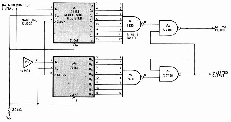
-------------- Tap dance. By changing the quantity and position of
the shift register outputs into which the multiple-input NAND gates tap,
a designer can mask unwanted spikes, as well as exercise a wide range
of control over the output pulse width and rising and falling pulse edges.
Low-cost generator delivers all standard bit rates
by Robert E. Turner Martian Technologies, Spring Valley, Calif.
Costing only $2, this generator can drive universal asynchronous receiver-transmitters and other RS-232 serial interface chips at any standard bit rate selected by the user. It is especially suitable for systems based on the Z80 microprocessor from which the generator can derive its 4-megahertz quartz-crystal time base.
As the figure shows, a 4-MHz input clock is divided by 13 by the 74LS393 counter (A1) and a 74LS11 AND gate, thereby providing a 3.25-microsecond signal that is suitable for driving the CD4024 seven-stage counter, A2.
This signal is close to 16 times the maximum 19.2 kilobit/s output frequency. Smaller divisions are handled by the counter, which supplies 9,600-, 4,800-, 2,400-, 1,200-, 600-, 300-, 150-, and 110-b/s outputs.
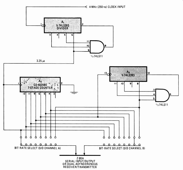
------------ Trimmed taps. With a Z80 system clock trimming costs
to $2, the four-chip generator delivers all standard bit rates for RS-232-based
systems. The generated rate accuracy is high (see table). The system
can be easily modified for older interfaces.
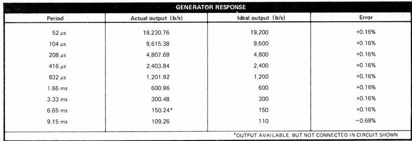
----- GENERATOR RESPONSE -----
The counter outputs are wired so that a bit rate may be selected for both channels of a Z80A serial input/output module or dual asynchronous receiver-transmitter serial interface chip. The output frequency of the generator is 16 times greater than the bit rate, so each serial data bit is sampled 16 times per bit period.
The bit-rate clock frequency is selected with either printed-circuit-board jumpers or by small dual-in line-packaged switches. The entire circuit is small enough to be mounted next to the Z80's DB-25 connectors that are mounted on its rear panel, making it easy for the end user of the RS-232 interface to select a bit rate. The dual-channel version of the circuit requires only five interface lines: the 4-MHz clock input, bit-rate clock A and B outputs, the 5-volt line, and logic ground.
As for the accuracy of the rates generated, they are well within the 1% timing variation standard required by the RS-232 interface (see table). The generator has been used with many different terminals and printers, and no operating difficulties have been encountered.
The circuit may also be used with most of the older serial interface chips like the 8251 and the 6850, if the user is willing to sacrifice the 19.2-kb/s output. In this case, the divide-by-11 counter would be driven by a 2-MHz clock, with the highest bit rate available becoming 9.6-kb/s. This signal drives the counter. The output of the counter that divides the 110-b/s signal by 11 (counter A3) would then be connected to the new 1,200 b/s output of the seven-stage counter.
[source: ISBN 0-07-606808-0]