In this Section we shall examine two additional methods* which have been employed to achieve frequency modulation directly by means of a reactance modulator. In one method, the modulator is a diode. In the second system, advantage is taken of the fact that the input capacitance of a tube is dependent on its mutual conductance. Each approach, in its way, is distinctive and demonstrates the versatility of the direct method.
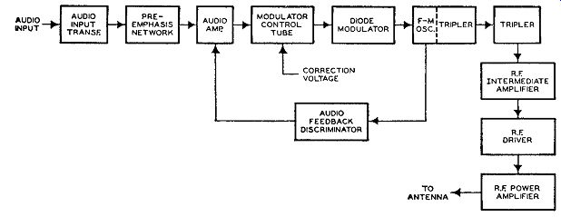
FIG. 15.1. A block diagram of an FM transmitter in which the frequency
of the master oscillator is varied by a diode modulator. The frequency
stabilization system which supplies the above correction voltage is shown
in Fig. 15.5.
* Commercial FM transmitters using both modulation methods to be described are in operation today.
Direct FM with Diode Modulator. A block diagram of a transmitter using a diode modulator is shown in Fig. 15.1. The audio circuits, to the point where their signal is applied to the modulator control tube, are conventional. An audio feedback discriminator, which is peculiar to this circuit, tends to stabilize the audio stages by applying a small amount of inverse feedback voltage. The operation of this circuit is simple and will be analyzed after the operation of the modulating system has been investigated.
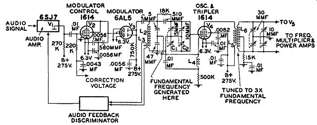
Fig. 15.2. The modulator and oscillator circuits of the transmitter
shown in Fig. 15.1.
The oscillator, using a 1614 beam-power tetrode, is connected as an electron-coupled Colpitts oscillator and tripler circuit. (See Fig. 15.2.) The grid circuit generates a frequency ½ that of the transmitted carrier frequency. This frequency is tripled in the plate circuit of the oscillator tube to 1/2 the output frequency. The grid circuit of V4 is tuned by the grid inductance, L2 , by the coarse and fine variable capacitors, C1 and C2 , and by the capacitative reactance of the modulator tube, V3. In the plate circuit, L5 in conjunction with L6 forms a tuned coupling circuit having a very large coefficient of coupling. Tuning here is accomplished by the grid tuning capacitors of the following R.F. tripler stage. The final frequency multiplication (3 times) is achieved in the plate circuit of the following tube, V5 (not shown). The frequency, at this point, is equal to the carrier frequency authorized to that station.
Beyond V5, intermediate and power amplifiers increase the power of the signal until it has attained the full value at which the station operates.
Modulating Circuits. The modulator circuit consists of two tubes, a 1614 beam-power tetrode and a 6AL5 duo-diode. The 1614 is connected as a triode and operates as a class A audio frequency amplifier. The 6AL5, with both sections connected in parallel, is placed in series with the plate of the 1614. Hence the instantaneous current through the diode depends upon the current flowing through the 1614. Since the 1614 is operating as a class A amplifier, its plate current and that of the diode will always be proportional to the applied audio signal.
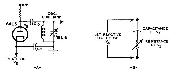
FIG. 15.3. (A) The diode modulator is connected across the grid inductance
of the oscillator. (B) Equivalent circuit of diode showing its electrical
effect on oscillator tank circuit.
The diode, in addition, is connected across the grid inductance of the oscillator. (See Fig. 15.3A.) This means that the interelectrode capacitance existing between cathode and plate of the diode and the tube's internal plate resistance are also shunted across the oscillator tank circuit. (See Fig. 15.3B.) By varying the value of this plate resistance, we change the overall reactance of the network, which, in turn, causes the frequency of the oscillator to change. Thus, the audio voltage at the grid of V2, by varying the current flowing through this tube and the diode, will also vary the reactive effect of the diode on the oscillator.
To prevent amplitude modulation as well as frequency modulation, the
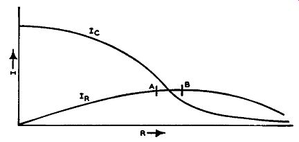
FIG. 15.4. Resistive and reactive current in diode modulator.
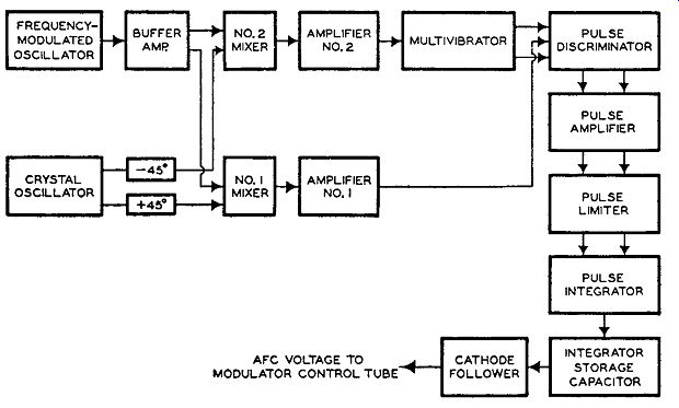
FIG. 15.5. A block diagram of the frequency stabilization system employed
in the FM transmitter of Fig. 15.1.
6AL5 is operated at a point where the change in resistive current through the tube is very small in proportion to the change in capacitative current.
A plot of the current through the 6AL5 tube is shown in Fig. 15.4. It will be noted that, between the points A and B, a very small change in resistive current, IR, occurs for a relatively large change in the resistive effect of the tube. At the same time, between these two points, the change in capacitative current, le, is quite large. Hence, by operating the diode between points A and B, we secure frequency modulation accompanied by only a negligible amount of amplitude modulation.
Audio Feedback Discriminator. The purpose of the audio feedback discriminator is to provide an inverse feedback voltage for the audio amplifier, V1 , in order to stabilize its operation and to reduce distortion. The discriminator circuit is, in essence, a Foster-Seeley FM detector. The primary and secondary windings of the discriminator transformer are tuned to the frequency of the master oscillator, V4. A small coupling link, L3 , transfers the signal from the oscillator grid coil to the discriminator trans former. When the oscillator is unmodulated, the output of the discriminator will be zero. This action is in accordance with the operation of a discriminator circuit. However, when an audio voltage is being applied to the circuit, the oscillator signal becomes frequency-modulated, and a similar audio voltage is obtained from the discriminator. This voltage possesses the proper phase to be applied to the grid of V 1 as an inverse feedback voltage.
Frequency Stabilization Circuits. We come now to the frequency stabilization circuits, these being necessary in all reactance-modulated FM transmitters. In the previous Section, one system using motor control, one system employing a discriminator, and one system using a phase detector were described. The present system represents still another approach, using a series of pulses and a pulse-counting circuit to keep the transmitter on frequency. When the master oscillator drifts to one side of its assigned frequency, the output pulses of the circuit have one polarity; when the drift is to the other side of the assigned frequency, the pulse polarity reverses.
A block diagram of the entire frequency stabilizer section is shown in Fig. 15.5. The master oscillator feeds a portion of its signal to two separate mixers through a buffer amplifier. The same amount of voltage is applied, in phase, to each mixer. At the same time a crystal oscillator, operating at the exact frequency to which the master oscillator should be set, also feeds its voltage to each of the mixers. However, the crystal oscillator output must first pass through two resistance-capacitance phase shift networks so designed that the crystal oscillator voltage reaching mixer No. 1 is advanced 45° in phase while the voltage reaching mixer No. 2 is retarded by 45°. The two voltages, then, are actually 90° out of phase.
Within each mixer, the signals from the crystal and master oscillators mix, and if the two are not equal in frequency, the difference and sum of these frequencies will be generated. Of interest in this discussion are the difference frequencies since the sum frequencies are by-passed to ground.
Any output frequencies developed in the mixers will be equal, but the phase of the voltage from mixer No. 2 will differ from that of mixer No. 1 by 90° because of the phase difference in the applied crystal oscillator voltages.
Let us examine this latter point in greater detail. When the master oscillator is operating at its propercenter frequency, then its frequency and that of the crystal oscillator will be equal. Under these conditions, no difference frequency voltage will be obtained at the output of either mixer.
However, when the two oscillator frequencies do not agree, the following will happen.
1. When the oscillator frequency is higher than the crystal reference frequency, the output of mixer No. 2 will lead the output of mixer No. 1 by 90°.
2. When the oscillator frequency is lower than the crystal reference frequency, the output of mixer No. 2 will lag the output of mixer No. 1 by 90°. Fig. 15.6 illustrates these phase relationships, with the output of mixer No. 1 kept constant while the output of mixer No. 2 lags or leads by 90°. During modulation of the master oscillator, the applied audio-modulating voltage will swing the oscillator frequency above and below its operating point. This means that during the positive half of an audio frequency cycle, when the carrier shifts (in this circuit) in the low frequency direction, the output of mixer No. 1 will lead the voltage output of No. 2. During the negative half of the audio cycle, the output of mixer No. 1 will lag the out- put of mixer No. 2. If the center operating frequency of the master oscillator is properly set, no correction voltage will be developed by the frequency stabilization network. However, if the master oscillator is not properly centered and has instead drifted to one side, then a difference frequency will appear in the mixer plate circuits even when no audio voltage is being applied to the circuit. When, now, an audio voltage is applied, the outputs of the mixers will not lead and lag for an equal length of time as they did when the master oscillator was on frequency. This will result in a correction voltage being developed by the stabilization system which will act to return the oscillator to its propercenter frequency.
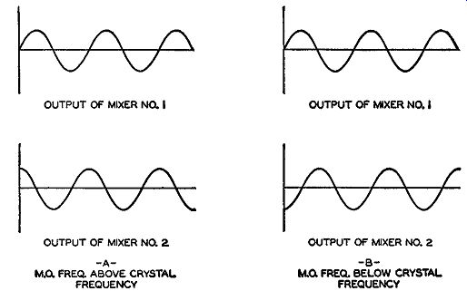
Fig. 15.6. The phase relationship between the outputs of mixers 1 and
2 when the master oscillator is not operating at its assigned center
frequency.
The output of each mixer is fed to a separate amplifier. The output of mixer No. 1 is fed to amplifier No. 1. This tube is biased practically to cut off and acts to square off the applied sine wave, giving it the shape shown in Fig. 15.7. This wave is then applied to the center of the following pulse discriminator.
The output of mixer No. 2 is passed through amplifier No. 2 and then used to trigger a multivibrator. Although it is beyond the scope of this text to go into the operation of multivibrators, it can be said that this circuit, containing two tubes, transforms the sine-wave output of amplifier No. 2 into a series of square waves. These square waves are then passed through a resistance-capacitance network which converts them into a series of positive and negative pulses. It is these pulses which are received by the same pulse discriminator to which the amplified output of mixer No. 1 is applied.
Note that the pulse discriminator receives equal and oppositely phased pulses from the multivibrator. This is required because of the manner in which these voltages are applied to the pulse discriminator.
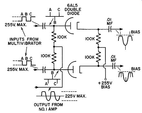
Fig. 15.7. The pulse discriminator circuit.
Pulse Discriminator. The purpose of the pulse discriminator is to combine the output of the multivibrator with the amplified output from mixer No. 1 in such a manner that voltage pulses appear on one side of its output circuit when the master oscillator is above its correct center operating frequency and on the other side of the output circuit when the oscillator frequency is below its correct operating frequency. If the master oscillator is on frequency, then during audio modulation, the number of pulses appearing on one side of the discriminator during one half cycle of audio voltage will be exactly equal to the number of pulses appearing on the other side of the discriminator, during the next half cycle. However, this will not be true if the master oscillator has drifted.
The pulse discriminator consists of two diodes, the cathode of each being biased by a positive 255 volts. The maximum possible signal voltage avail able from amplifier No. 1 is also +255 volts, and therefore the voltage due solely to amplifier No. 1 cannot cause the discriminator to pass current.
The same is true of the voltage pulses obtained from the multivibrator.
However, when both voltages appear at the same time and add in the positive direction, current will flow. The voltage will add together on one side of the discriminator when one mixer voltage leads, and on the other side of the discriminator ·when the voltage from the other mixer leads.
Note that, whenever one of the diodes conduct, only the voltage pips riding atop the wave from amplifier No. 1 appear in the output. If the voltages oppose each other, nothing appears at that side of the discriminator.
The positive pulses appearing on either side of the discriminator are kept separate from each other and are passed through separate pulse amplifiers and a pulse limiter. These stages bring all pulses to the same amplitude, removing any variations that might possibly exist between them. The pulses are then applied to a pulse integrator circuit in such fashion that half of the integrator responds to the pulses appearing on one side of the circuit and half of the integrator responds to the pulses appearing on the other side of the circuit. The currents flowing through the first half of the integrator charge a capacitor in one direction while the currents flowing through the second half of the integrator charge the same capacitor in the opposite direction. The voltage developed across the capacitor is then applied through a cathode follower to the modulator control tube where it can alter the center or resting frequency of the modulated oscillator.
When the master oscillator is on frequency, the average voltage developed across the capacitor over one audio cycle is zero. For all other conditions either a positive or negative resultant voltage will appear across the capacitor which, when applied to the modulator control circuit, will act to bring the master oscillator back on frequency.
In spite of the apparent complexity of this circuit, it is simple to operate because it requires no adjustments once it has been placed in operation.
There are no tuned circuits, frequency dividers, or locked-in oscillators.
Most tubes operate from cut-off to saturation, reducing to a minimum the effect of any variation in tube characteristics. Actually, under these conditions, the only positive manner in which a tube can interfere with the proper circuit operation is by complete failure, and generally tubes are removed from the circuit, during periodic inspections, long before this occurs.
FM by TUBE CAPACITANCE VARIATION
In still another approach to direct frequency modulation, advantage is taken of the fact that the input capacitance of a tube is dependent upon its mutual conductance. The mutual conductance, in turn, will vary as the plate current varies and, going one step farther, this will depend upon the grid voltage. Thus, tying all these facts together, we have a direct connection between the grid voltage of the tube (in this instance, the modulator tube) and the input capacitance of the tube. If, therefore, we apply an audio voltage to the modulator grid, we can cause the input capacitance of the tube to vary at an audio rate. By connecting the tuned circuit of an oscillator across the grid of the modulator tube, we effectively shunt this input capacitance across the oscillator and cause the generated frequency to vary in step with the applied audio voltage. The result is frequency modulation.
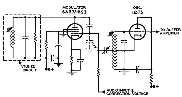
Fig. 15.8A. A simplified diagram of the modulator and oscillator used
in a transmitter where FM is obtained by varying the input capacitance.
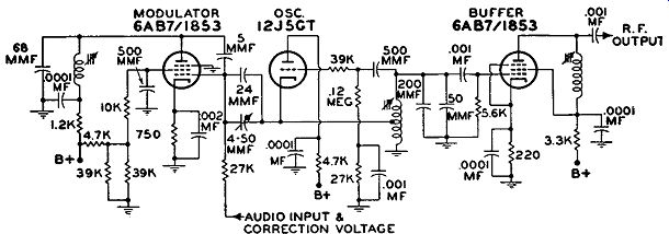
Fig. 15.8B. The complete schematic of the modulator and oscillator.
Shown, too, is the buffer which follows the oscillator.
The basic and actual circuits of a suitable modulator and oscillator are shown in Fig. 15.8. The oscillator uses a 12J5GT triode arranged to operate as a conventional Hartley. Connected across part of the oscillator tank inductance is the modulator tube, a 6AB7 /1853 pentode. This particular tube was chosen because it possesses a high gm value and because this gm can be made to vary linearly with grid voltage. The latter qualification is necessary to insure that the frequency modulation produced is directly proportional to the applied audio-modulating signal.
It can be shown by a rather lengthy mathematical analysis that the in put capacitance of an amplifier tube is given by
c. = Cgk + Cgp(l + A)
where ... C1 = input capacitance of amplifier tube
Cuk = grid-to-cathode capacitance of tube
Cup = grid-to-plate capacitance of tube
A = gain of the tube
For all practical purposes, Cuk and Cup are constant and will not change appreciably with tube current. The gain, on the other hand, will vary with tube current because, for a pentode, the gain, A, can be shown to be equal to gmZL where g_m is the mutual conductance of the tube and ZL is the load impedance into which the tube works. Hence, the foregoing equation can be rewritten in the form Ci= Cgk + Cgp(l + g_mZL)
Note that C, is not only affected by the g_m of the modulator tube, but also by Zr,, the load impedance of this tube. In order to have C, affected only by g_m, the plate load is made resistive by using a resonant circuit, which is resistive at its resonant frequency. A resistor is shunted across the resonant circuit in order to have it tune broadly and therefore remain in resonance over the range of frequencies covered by the oscillator when it is frequency-modulated. With this circuit modification, the equation for the input capacitance of the modulator becomes:
Ci= Cgk + Cgp(l + g_mRL)
where Rr, now represents the load impedance.
Since the 6AB7/1853 modulator tube is pentode, the Cup of this tube is very small, on the order of 0.015 mmf, and its effect, in comparison to Cuk (which is 15 mmf) would be almost negligible. To overcome this, a 5-mmf capacitance is shunted across the tube, from plate to grid providing sufficient input capacitance variation with changes in audio signal. Another capacitor, this one variable, connects the grid of the modulator tube to the tuning inductance of the oscillator. Its purpose is to provide a fixed frequency swing for a given change in audio voltage. To prevent too much R.F. signal from appearing on the modulator grid, this variable capacitance is connected to a tap on the tank inductance.
The audio voltage is applied to the grid of the modulator tube, and as it varies the current through the tube the g_m will change and with it the value of the input capacitance. The center frequency of the oscillator is set at some value between 3.66 and 4.5 mhz, so that with a frequency multiplication of 24 (3 doublers and a tripler) the transmitted carrier frequency ends up between 88 and 108 mhz. The 75- khz deviation for 100 percent modulation is 75/24 or 3.12 khz at the oscillator frequency.
The sequence of low-power stages beyond the modulated oscillator consists of a series of three doublers and a tripler, at which point the signal frequency is between 88 to 108 mhz. (See Fig. 15.9.) The signal is now transferred to a buffer and an intermediate power amplifier where its power is increased to 250 watts. Beyond this point, power amplifiers raise the signal power to 1, 3, 10, 20, or 50 kw, depending upon the authorized power for the particular station.
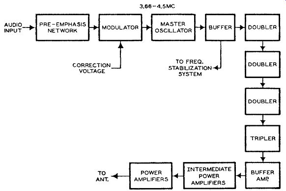
Fig. 15.9. A block diagram of the R.F. stages of an FM transmitter employing
the modulating circuit of Fig. 15.8.
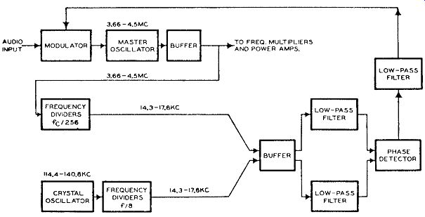
Fig. 15.10. A block diagram of the frequency stabilization system employed
in the FM transmitter of Fig. 15.9.
Frequency Stabilization System. To maintain the master oscillator within 2000 cycles of its assigned frequency (as required by the F.C.C.) a frequency stabilization system is incorporated into this transmitter. A block diagram of this system is shown in Fig. 15.10. The frequency output from a buffer immediately following the frequency-modulated oscillator is fed to a frequency-divider chain where the 3.66 - 4.5 mhz frequency is divided 256 times to a frequency between 14.3 - 17.6 khz. (It is understood that only one center frequency will be obtained from the master oscillator and consequently only one frequency will appear at the end of the divider chain.) At the same time, a crystal oscillator, operating at some frequency between 114.4 khz and 140.8 khz, has its signal pass through two frequency divider stages where the initial frequency is lowered by a factor of 8 (2 X 4). This will produce a frequency between 14.3 and 17.6 khz, or the same frequency that the master oscillator should produce at the end of its frequency chain if it is exactly on frequency. The two divided signals are then passed through separate buffer amplifiers and low-pass filters and applied to the phase detector. The latter stage is identical with the phase detector described in Fig. 14.20.
EXAM
1. Explain the function of each block in Fig. 15.1.
2. How is modulation achieved in this FM transmitter? Describe in detail, using simple schematic circuits.
3. What is the purpose of the audio feedback discriminator in the transmitter of Fig. 15.1?
4. Draw a block diagram of the frequency stabilization system used in this transmitter.
5. Explain briefly the operation of the frequency stabilization system.
6. In what way does the FM transmitter of Fig. 15.9 make use of the fact that the input capacitance of a tube is dependent upon the mutual conductance of that tube? Explain fully.
7. Draw a simple schematic circuit of the modulator and master oscillator of this transmitter (Fig. 15.9).
8. What type of frequency stabilization system does the FM transmitter of Fig. 15.9 employ? Illustrate with a block diagram.
9. Would it be possible to interchange the frequency stabilization system employed in the transmitter of Fig. 15.1 for the unit used in the transmitter of Fig. 15.9? Explain fully, indicating what changes might be required in the stabilization circuit frequencies or components, if any.
10. What factors govern the input capacitance of an amplifier tube? Give the mathematical relationship that pertains.
+++++++++++