PREAMPLIFIER STAGES
The popular concept of hi-fi attributes the major role in final sound quality to the audio power amplifier and the output devices or output configuration which it uses. Yet in reality the pre-amplifier system, used with the power amplifier, has at least as large an influence on the final sound quality as the power amplifier, and the design of the voltage gain stages within the pre- and power amplifiers is just as important as that of the power output stages. Moreover, it’s developments in the design of such voltage amplifier stages which have allowed the continuing improvement in amplifier performance.
The developments in solid-state linear circuit technology which have occurred over the past thirty years seem to have been inspired in about equal measure by the needs of linear integrated circuits, and by the demands of high-quality audio systems, and engineers working in both of these fields have watched each other's progress and borrowed from each other's designs.
In general, the requirements for voltage gain stages in both audio amplifiers and integrated-circuit operational amplifiers are very similar.
These are that they should be linear, which implies that they are free from waveform distortion over the required output signal range, have as high a stage gain as is practicable, have a wide AC bandwidth and a low noise level, and are capable of an adequate output voltage swing.
The performance improvements which have been made over this period have been due in part to the availability of new or improved types of semiconductor device, and in part to a growing understanding of the techniques for the circuit optimization of device performance. It’s the interrelation of these aspects of circuit design which is considered below.
LINEARITY
Bipolar transistors
In the case of a normal bipolar (NPN or PNP) silicon junction transistor , for which the chip cross-section and circuit symbol is shown in FIG. 1, the major problem in obtaining good linearity lies in the nature of the base voltage/collector current transfer characteristic, shown in the case of a typical '???' device (a '???' device would have a very similar characteristic, but with negative voltages and currents) in FIG.
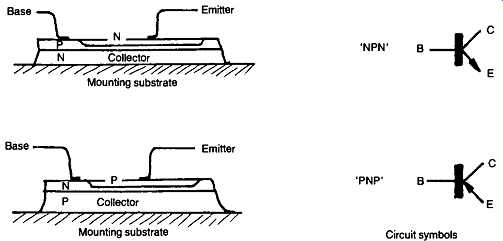 FIG. 1 Typical chip cross-section of NPN and PNP silicon planar epitaxial
transistors.
FIG. 1 Typical chip cross-section of NPN and PNP silicon planar epitaxial
transistors.
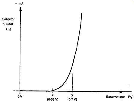
FIG. 2 Typical transfer characteristic of silicon transistor. Base voltage
(Vb)
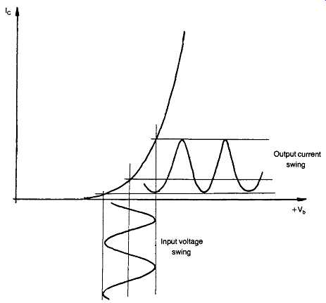
FIG. 3 Transistor amplifier waveform distortion due to transfer characteristics.
In this, it can be seen that the input/output transfer characteristic is strongly curved in the region 'X - Y' and an input signal applied to the base of such a device, which is forward biased to operate within this region, would suffer from the very prominent (second harmonic) waveform distortion shown.
The way this type of non-linearity is influenced by the signal output level is shown in FIG. 4. It’s normally found that the distortion increases as the output signal increases, and conversely.
There are two major improvements in the performance of such a bipolar amplifier stage which can be envisaged from these characteristics.
Firstly, since the non-linearity is due to the curvature of the input characteristics of the device - the output characteristics, shown in FIG. 5, are linear - the smaller the input signal which is applied to such a stage, the lower the non-linearity, so that a higher stage gain will lead to reduced signal distortion at the same output level. Secondly, the distortion due to such a stage is very largely second harmonic in nature.
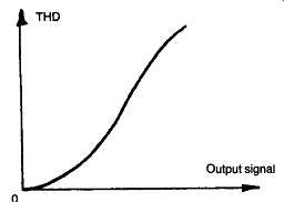
FIG. 4 Relationship between signal distortion and output signal voltage
in bipolar transistor amplifier.
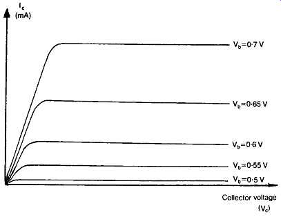
FIG. 5 Output current/voltage characteristics of typical silicon bipolar
transistor.
This implies that a 'push-pull' arrangement, such as the so-called long tailed pair circuit shown in FIG. 6, which tends to cancel second harmonic distortion components, will greatly improve the distortion characteristics of such a stage.
Also, since the output voltage swing for a given input signal (the stage gain) will increase as the collector load (R2 in FIG. 6) increases, the higher the effective impedance of this, the lower the distortion which will be introduced by the stage, for any given output voltage signal.
If a high value resistor is used as the collector load for Qt in FIG. 6, either a very high supply line voltage must be applied, which may exceed the voltage ratings of the devices or the collector current will be very small, which will reduce the gain of the device, and therefore tend to diminish the benefit arising from the use of a higher value load resistor.
Various circuit techniques have been evolved to circumvent this problem, by producing high dynamic impedance loads, which nevertheless permit the amplifying device to operate at an optimum value of collector current.
These techniques will be discussed below.
An unavoidable problem associated with the use of high values of collector load impedance as a means of attaining high stage gains in such amplifier stages is that the effect of the 'stray' capacitances, shown as Cs in FIG. 7, is to cause the stage gain to decrease at high frequencies as the impedance of the stray capacitance decreases and progressively begins to shunt the load. This effect is shown in FIG. 8, in which the 'transition' frequency, f0, (the - 3 dB gain point) is that frequency at which the shunt impedance of the stray capacitance is equal to that of the load resistor, or its effective equivalent, if the circuit design is such that an 'active load' is used in its place.
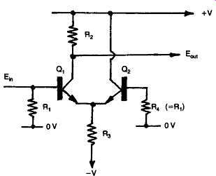
FIG. 6 Transistor voltage amplifier using long-tailed pair circuit layout.
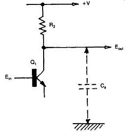
FIG. 7 Circuit effect of stray capacitance.
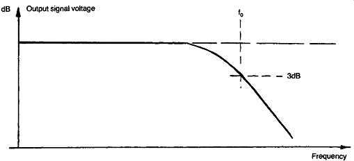
FIG. 8 Influence of circuit stray capacitances on stage gain.
Field effect devices
Other devices which may be used as amplifying components are field effect transistors and MOS devices. Both of these components are very much more linear in their transfer characteristics but have a very much lower mutual conductance (Gm). This is a measure of the rate of change of output current as a function of an applied change in input voltage. For all bipolar devices, this is strongly dependent on collector current, and is , for a small signal silicon transistor, typically of the order of 45 mA/V, per mA collector current.
Power transistors, operating at relatively high collector currents , for which a similar relationship applies, may therefore offer mutual conductances in the range of amperes/volt.
Since the output impedance of an emitter follower is approximately 1/Gm, power output transistors used in this configuration can offer very low values of output impedance, even without externally applied negative feedback.
All field effect devices have very much lower values for Gm, which will lie , for small-signal components, in the range 2-10 mA/V, not significantly affected by drain currents. This means that amplifier stages employing field effect transistors, though much more linear, offer much lower stage gains, other things being equal.
The transfer characteristics of junction (bipolar) FETs, and enhancement and depletion mode MOSFETS are shown in Figs 9(a), (b) and (c). MOSFETs FIG. 9 Gate voltage versus drain current characteristics of field effect devices.
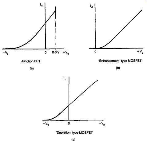
FIG. 10 Chip cross-section and circuit symbol for lateral MOSFET (small
signal type) --- Substrate and mount (Source connected to substrate)
N-ch MOSFET
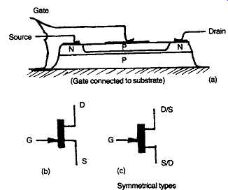
FIG. 11 Chip cross-section and circuit symbols for (bipolar) junction FET.
MOSFETs, in which the gate electrode is isolated from the source/drain channel, have very similar transfer characteristics to that of junction FETs. They have an advantage that, since the gate is isolated from the drain/source channel by a layer of insulation, usually silicon oxide or nitride, there is no maximum forward gate voltage which can be applied - within the voltage breakdown limits of the insulating layer. In a junction FET the gate, which is simply a reverse biased PN diode junction, will conduct if a forward voltage somewhat in excess of 0.6 V is applied.
The chip constructions and circuit symbols employed for small signal lateral MOSFETs and junction FETs (known simply as FETs) are shown in Figs 10 and 11.
It’s often found that the chip construction employed for junction FETs is symmetrical, so that the source and drain are interchangeable in use.
For such devices the circuit symbol shown in FIG. 11(c) should properly be used.
A practical problem with lateral devices, in which the current flow through the device is parallel to the surface of the chip, is that the path length from source to drain, and hence the device impedance and current carrying capacity, is limited by the practical problems of defining and etching separate regions which are in close proximity, during the manufacture of the device.
V-MOS AND T-MOS
This problem is not of very great importance for small signal devices, but it’s a major concern in high current ones such as those employed in power output stages. It has led to the development of MOSFETs in which the current flow is substantially in a direction which is vertical to the surface, and in which the separation between layers is determined by diffusion processes rather than by photo-lithographic means.
Devices of this kind, known as V-MOS and T-MOS constructions, are shown in Figs 12(a) and (b). Although these were originally introduced for power output stages, the electrical characteristics of such components are so good that these have been introduced, in smaller power versions, specifically for use in small signal linear amplifier stages. Their major advantages over bipolar devices, having equivalent chip sizes and dissipation ratings, are their high input impedance, their greater linearity, and their freedom from 'hole storage' effects if driven into saturation.
These qualities are increasingly attracting the attention of circuit designers working in the audio field, where there is a trend towards the design of amplifiers having a very high intrinsic linearity, rather than relying on the use of negative feedback to linearize an otherwise worse design.
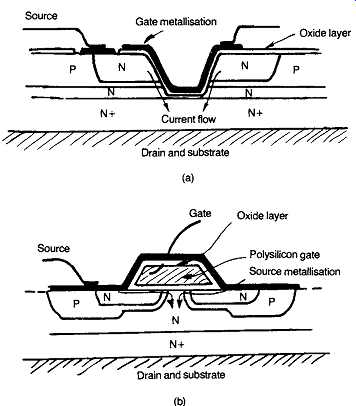
FIG. 12 Power MOSFET constructions using (a) V and (b) T configurations.
(Practical devices will employ many such cells in parallel.)
BREAKDOWN
A specific problem which arises in small signal MOSFET devices is that, because the gate-source capacitance is very small, it’s possible to induce breakdown of the insulating layer, which destroys the device, as a result of transferred static electrical charges arising from mishandling.
Though widely publicized and the source of much apprehension, this problem is actually very rarely encountered in use, since small signal MOSFETs usually incorporate protective zener diodes to prevent this eventuality, and power MOSFETs, where such diodes may not be used because they may lead to inadvertent 'thyristor' action, have such a high gate-source capacitance that this problem does not normally arise.
In fact, when such power MOSFETs do fail, it’s usually found to be due to circuit design defects, which have either allowed excessive operating potentials to be applied to the device, or have permitted inadvertent VHF oscillation, which has led to thermal failure.
NOISE LEVELS
Improved manufacturing techniques have lessened the differences between the various types of semiconductor device, in respect of intrinsic noise level. For most practical purposes it can now be assumed that the characteristics of the device will be defined by the thermal noise figure of the circuit impedances. This relationship is shown in the graph of Fig. 13.
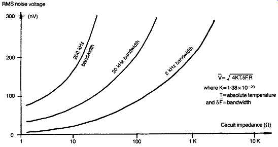
FIG. 13 Thermal noise output as a function of circuit impedance.
For very low noise systems, operating at circuit impedance levels which have been deliberately chosen to be as low as practicable - such as in moving coil pick-up head amplifiers -- bipolar junction transistors are still the preferred device. These will either be chosen to have a large base junction area, or will be employed as a parallel-connected array; as , for example, in the LM194/394 'super-match pair' ICs, where a multiplicity of parallel connected transistors are fabricated on a single chip, giving an effective input (noise) impedance as low as 40 ohms.
However, recent designs of monolithic dual J-FETs, using a similar type of multiple parallel-connection system, such as the Hitachi 2SK389, can offer equivalent thermal noise resistance values as low as 33 ohms, and a superior overall noise figure at input resistance values in excess of 100 ohms.
At impedance levels beyond about 1 kilo-ohm there is little practical difference between any devices of recent design. Earlier MOSFET types were not so satisfactory, due to excess noise effects arising from carrier trapping mechanisms in impurities at the channel/gate interface.
OUTPUT VOLTAGE CHARACTERISTICS
Since it’s desirable that output overload and signal clipping don’t occur in audio systems, particularly in stages preceding the gain controls, much emphasis has been placed on the so-called 'headroom' of signal handling stages, especially in hi-fi publications where the reviewers are able to distance themselves from the practical problems of circuit design.
While it’s obviously desirable that inadvertent overload shall not occur in stages preceding signal level controls, high levels of feasible output voltage swing demand the use of high voltage supply rails, and this, in turn, demands the use of active components which can support such working voltage levels.
Not only are such devices more costly, but they will usually have poorer performance characteristics than similar devices of lower voltage ratings. Also, the requirement for the use of high voltage operation may preclude the use of components having valuable characteristics, but which are restricted to lower voltage operation.
Practical audio circuit designs will therefore regard headroom simply as one of a group of desirable parameters in a working system, whose design will be based on careful consideration of the maximum input signal levels likely to be found in practice.
Nevertheless, improved transistor or IC types, and new developments in circuit architecture, are welcomed as they occur, and have eased the task of the audio design engineer , for whom the advent of new program sources, in particular the compact disc, and now digital audio tape systems, has greatly extended the likely dynamic range of the output signal.
Signal characteristics
The practical implications of this can be seen from a consideration of the signal characteristics of existing program sources. Of these, in the past, the standard vinyl ('black') disc has been the major determining factor. In this, practical considerations of groove tracking have limited the recorded needle tip velocity to about 40 cm/s, and typical high-quality pick-up cartridges capable of tracking this recorded velocity will have a voltage output of some 3 mV at a standard 5 cm/s recording level.
If the pre-amplifier specification calls for maximum output to be obtain able at a 5 cm/s input, then the design should be chosen so that there is a 'headroom factor' of at least 8x, in such stages preceding the gain controls.
In general, neither FM broadcasts, where the dynamic range of the transmitted signal is limited by the economics of transmitter power, nor cassette recorders, where the dynamic range is constrained by the limited tape overload characteristics, have offered such a high practicable dynamic range.
It’s undeniable that the analogue tape recorder, when used at 15 in./s, twin-track, will exceed the LP record in dynamic range. After all, such recorders were originally used for mastering the discs. But such program sources are rarely found except among live recording' enthusiasts. However, the compact disc, which is becoming increasingly common among purely domestic hi-fi systems, presents a new challenge, since the practicable dynamic range of this system exceeds 80 dB (10000:1), and the likely range from mean (average listening level) to peak may well be as high as 35 dB (56:1) in comparison with the 18 dB (8:1) range likely with the vinyl disc.
Fortunately, since the output of the compact disc player is at a high level, typically 2 V RMS, and requires no signal or frequency response conditioning prior to use, the gain control can be sited directly at the input of the preamp. Nevertheless, this still leaves the possibility that signal peaks may occur during use which are some 56 x greater than the mean program level, with the consequence of the following amplifier stages being driven hard into overload.
This has refocused attention on the design of solid state voltage amplifier stages having a high possible output voltage swing, and upon power amplifiers which either have very high peak output power ratings, or more graceful overload responses.
VOLTAGE AMPLIFIER DESIGN
The sources of non-linearity in bipolar junction transistors have already been referred to, in respect of the influence of collector load impedance, and push-pull symmetry in reducing harmonic distortion. An additional factor with bipolar junction devices is the external impedance in the base circuit, since the principal non-linearity in a bipolar device is that due to its input voltage/output current characteristics. If the device is driven from a high impedance source, its linearity will be substantially greater, since it’s operating under conditions of current drive.
This leads to the good relative performance of the simple, two-stage, bipolar transistor circuit of FIG. 14, in that the input transistor, Q1 is only required to deliver a very small voltage drive signal to the base of Q2, so the signal distortion due to Q1 will be low. Q2, however, which is required to develop a much larger output voltage swing, with a much greater potential signal non-linearity, is driven from a relatively high source impedance, composed of the output impedance of Q which is very high indeed, in parallel with the base-emitter resistor, R4. R1, R2, and R3/C2 are employed to stabilize the DC working conditions of the circuit.
Normally, this circuit is elaborated somewhat to include both DC and AC negative feedback from the collector of Q2 to the emitter of Q,, as shown in the practical amplifier circuit of FIG. 15.
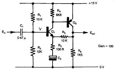
FIG. 14 Two-stage transistor voltage amplifier.
FIG. 15 Practical two-transistor feedback amplifier.
This is capable of delivering a 14 V p-p output swing, at a gain of 100, and a bandwidth of 15 Hz to 250 kHz, at -3 dB points; largely determined by the value of C2 and the output capacitances, with a THD figure of better that 0.01% at 1 kHz.
The practical drawbacks of this circuit relate to the relatively low value necessary for R3 -- with the consequent large value necessary for C2 if a good LF response is desired, and the DC offset between point 'X' and the output, due to the base-emitter junction potential of d , and the DC voltage drop along R5, which makes this circuit relatively unsuitable in DC amplifier applications.
An improved version of this simple two-stage amplifier circuit is shown in FIG. 16, in which the single input transistor has been replaced by a 'long-tailed pair' configuration of the type shown in FIG. 16. In this, if the two-input transistors are reasonably well matched in current gain, and if the value of R3 is chosen to give an equal collector current flow through both Ch and Q2, the DC offset between input and output will be negligible, and this will allow the circuit to be operated between symmetrical (+ and - ) supply rails, over a frequency range extending from DC to 250 kHz or more.
Because of the improved rejection of odd harmonic distortion inherent in the input 'push-pull' layout, the THD due to this circuit, particularly at less than maximum output voltage swing, can be extremely low, and this probably forms the basis of the bulk of linear amplifier designs. However, further technical improvements are possible, and these are discussed below.
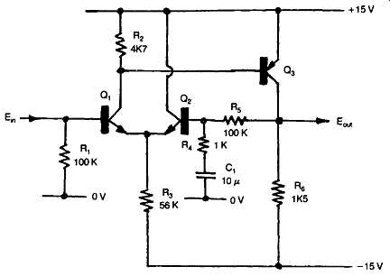
FIG. 16 Improved two-stage feedback amplifier.
CONSTANT-CURRENT SOURCES AND 'CURRENT MIRRORS'
As mentioned above, the use of high-value collector load resistors in the interests of high stage gain and low inherent distortion carries with it the penalty that the performance of the amplifying device may be impaired by the low collector current levels which result from this approach.
Advantage can, however, be taken of the very high output impedance of a junction transistor, which is inherent in the type of collector current/ supply voltage characteristics illustrated in FIG. 5, where even at currents in the 1-10 mA region, dynamic impedances of the order of 100 kilohms may be expected.
A typical circuit layout which utilizes this characteristic is shown in Fig. 17, in which R1 and R2 form a potential divider to define the base potential of C1, and R3 defines the total emitter or collector currents for this effective base potential.
This configuration can be employed with transistors of either PNP or NPN types, which allows the circuit designer considerable freedom in their application.
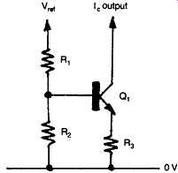
FIG. 17 Transistor constant current source.
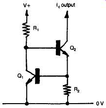
FIG. 18 Two-transistor constant current source.
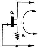
FIG. 19 Two-terminal constant current source.
An improved, two-transistor, constant current source is shown in Fig. 18. In this Rx is used to bias Q2 into conduction, and Qt is employed to sense the voltage developed across R2, which is proportional to emitter current, and to withdraw the forward bias from Q2 when that current level is reached at which the potential developed across R2 is just sufficient to cause Ch to conduct.
The performance of this circuit is greatly superior to that of FIG. 17, in that the output impedance is about 10x greater, and the circuit is insensitive to the potential, +Vref., applied to R1? so long as it’s adequate to force both Q2 and Q1 into conduction.
An even simpler circuit configuration makes use of the inherent very high output impedance of a junction FET under constant gate bias conditions. This employs the circuit layout shown in FIG. 19, which allows a true 'two-terminal' constant current source, independent of supply lines or reference potentials, and which can be used at either end of the load chain.
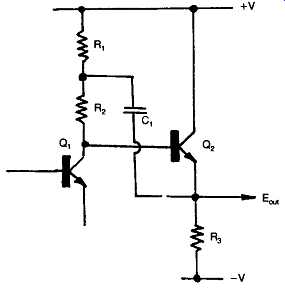
FIG. 20 Load impedance increase by boot-strap circuit.
The current output from this type of circuit is controlled by the value chosen for R1 and this type of constant current source may be constructed using almost any available junction FET, provided that the voltage drop across the FET drain-gate junction does not exceed the breakdown voltage of the device. This type of constant current source is also available as small, plastic-encapsulated, two-lead devices, at a relatively low cost, and with a range of specified output currents.
All of these constant current circuit layouts share the common small disadvantage that they won’t perform very well at low voltages across the current source element. In the case of Figs 17 and 18, the lowest practicable operating potential will be about 1 V. The circuit of FIG. 19 may require, perhaps, 2-3 V, and this factor must be considered in circuit performance calculations.
The 'boot-strapped' load resistor arrangement shown in FIG. 20, and commonly used in earlier designs of audio amplifier to improve the linearity of the last class AB amplifier stage (Q1), effectively multiplies the resistance value of R2 by the gain which Q2 would be deemed to have if operated as a common-emitter amplifier with a collector load of R3 in parallel with R1# This arrangement is the best configuration practicable in terms of available RMS output voltage swing, as compared with conventional constant current sources, but has fallen into disuse because it leads to slightly less good THD figures than are possible with other circuit arrangements.
All these circuit arrangements suffer from a further disadvantage, from the point of view of the integrated circuit designer: they employ resistors as part of the circuit design, and resistors, though possible to fabricate in IC structures, occupy a disproportionately large area of the chip surface.
Also, they are difficult to fabricate to precise resistance values without resorting to subsequent laser trimming, which is expensive and time consuming.
Because of this, there is a marked preference on the part of IC design engineers for the use of circuit layouts known as 'current mirrors', of which a simple form is shown in FIG. 21.
IC solutions
These are not true constant current sources, in that they are only capable of generating an output current (/out) which is a close equivalence of the input or drive current (7in). However, the output impedance is very high, and if the drive current is held to a constant value, the output current will also remain constant.
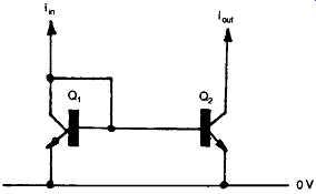
FIG. 21 Simple form of current mirror.
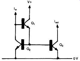
FIG. 22 Improved form of current mirror.
A frequently found elaboration of this circuit, which offers improvements in respect of output impedance and the closeness of equivalence of the drive and output currents, is shown in FIG. 22. Like the junction FET based constant current source, these current mirror devices are available as discrete, plastic-encapsulated, three-lead components, having various drive current/output current ratios , for incorporation into discrete component circuit designs.
The simple amplifier circuit of FIG. 16 can be elaborated, as shown in FIG. 23, to employ these additional circuit refinements, which would have the effect of increasing the open-loop gain, i.e. that before negative feedback is applied, by 10-100x and improving the harmonic and other distortions, and the effective bandwidth by perhaps 3-10x. From the point of view of the IC designer, there is also the advantage of a potential reduction in the total resistor count.
These techniques for improving the performance of semiconductor amplifier stages find particular application in the case of circuit layouts employing junction FETs and MOSFETs, where the lower effective mutual conductance values for the devices would normally result in relatively poor stage gain figures.
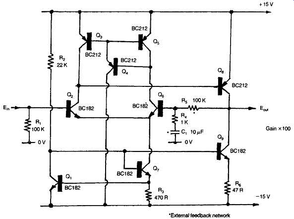
FIG. 23 Use of circuit elaboration to improve two-stage amplifier of FIG.
16.
This has allowed the design of IC operational amplifiers, such as the RCA CA3140 series, or the Texas Instruments TL071 series, which employ, respectively, MOSFET and junction FET input devices. The circuit layout employed in the TL071 is shown, by way of example, in FIG. 24.
Both of these opamp designs offer input impedances in the million megohm range - in comparison with the input impedance figures of 5-10 kilo-ohm which were typical of early bipolar ICs - and the fact that the input impedance is so high allows the use of such ICs in circuit configurations for which earlier op. amp. ICs were entirely inappropriate.
Although the RCA design employs MOSFET input devices which offer, in principle, an input impedance which is perhaps 1000 times better than this figure, the presence of on-chip Zener diodes, to protect the device against damage through misuse or static electric charges, reduces the input impedance to roughly the same level as that of the junction FET device.
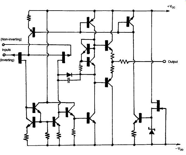
FIG. 24 Circuit layout of Texas Instruments TL071 opamp.
It’s a matter for some regret that the design of the CA3140 series devices is now so elderly that the internal MOSFET devices don’t offer the low level of internal noise of which more modern MOSFET types are capable. This tends rather to rule out the use of this MOSFET opamp for high quality audio use, though the TL071 and its equivalents such as the LF351 have demonstrated impeccable audio behavior.
PERFORMANCE STANDARDS
It has always been accepted in the past, and is still held as axiomatic among a very large section of the engineering community, that performance characteristics can be measured, and that improved levels of measured performance will correlate precisely, within the ability of the ear to detect such small differences, with improvements which the listener will hear in reproduced sound quality.
Within a strictly engineering context, it’s difficult to do anything other than accept the concept that measured improvements in performance are the only things which should concern the designer.
However, the frequently repeated claim by journalists and reviewers working for periodicals in the hi-fi field -- who, admittedly, are unlikely to be unbiased witnesses -- that measured improvements in performance don’t always go hand-in-hand with the impressions that the listener may form, tends to undermine the confidence of the circuit designer that the instrumentally determined performance parameters are all that matter.
It’s clear that it’s essential for engineering progress that circuit design improvements must be sought which lead to measurable performance improvements. Yet there is now also the more difficult criterion that those things which appear to be better, in respect of measured parameters, must also be seen, or heard, to be better.
Use of ICs
This point is particularly relevant to the question of whether, in very high quality audio equipment, it’s acceptable to use IC operational amplifiers, such as the TL071, or some of the even more exotic later developments such as the NE5534 or the OP27, as the basic gain blocks, around which the passive circuitry can be arranged, or whether, as some designers believe, it’s preferable to construct such gain blocks entirely from discrete components.
Some years ago, there was a valid technical justification for this reluctance to use op. amp. ICs in high quality audio circuitry, since the method of construction of such ICs was as shown, schematically, in FIG. 25, in which all the structural components were formed on the surface of a heavily T' doped silicon substrate, and relied for their isolation, from one another or from the common substrate, on the reverse biased diodes formed between these elements.
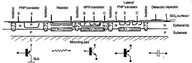
FIG. 25 Method of fabrication of components in silicon integrated circuit.
This led to a relatively high residual background noise level, in comparison with discrete component circuitry, due to the effects of the multiplicity of reverse diode leakage currents associated with every component on the chip. Additionally, there were quality constraints in respect of the components formed on the chip surface - more severe for some component types than for others - which also impaired the circuit performance.
A particular instance of this problem arose in the case of PNP transistors used in normal ICs, where the circuit layout did not allow these to be formed with the substrate acting as the collector junction. In this case, it was necessary to employ the type of construction known as a 'lateral PNP', in which all the junctions are diffused in, from the exposed chip surface, side by side.
In this type of device the width of the 'N' type base region, which must be very small for optimum results, depends mainly on the precision with which the various diffusion masking layers can be applied. The results are seldom very satisfactory. Such a lateral PNP device has a very poor current gain and HF performance.
In recent IC designs, considerable ingenuity has been shown in the choice of circuit layout to avoid the need to employ such unsatisfactory components in areas where their shortcomings would affect the end result. Substantial improvements, both in the purity of the base materials and in diffusion technology, have allowed the inherent noise background to be reduced to a level where it’s no longer of practical concern.
Modern standards
The standard of performance which is now obtainable in audio applications, from some of the recent IC op. amps - especially at relatively low closed-loop gain levels - is frequently of the same order as that of the best discrete component designs, but with considerable advantages in other respects, such as cost, reliability and small size.
This has led to their increasing acceptance as practical gain blocks, even in very high quality audio equipment.
When blanket criticism is made of the use of ICs in audio circuitry, it should be remembered that the 741 which was one of the earliest of these ICs to offer a satisfactory performance - though it’s outclassed by more recent types - has been adopted with enthusiasm, as a universal gain block , for the signal handling chains in many recording and broadcasting studios.
This implies that the bulk of the program signals employed by the critics to judge whether or not a discrete component circuit is better than that using an IC, will already have passed through a sizeable handful of 741-based circuit blocks, and if such ICs introduce audible defects, then their reference source is already suspect.
It’s difficult to stipulate the level of performance which will be adequate in a high-quality audio installation. This arises partly because there is little agreement between engineers and circuit designers on the one hand, and the hi-fi fraternity on the other, about the characteristics which should be sought, and partly because of the wide differences which exist between listeners in their expectations for sound quality or their sensitivity to distortions. These differences combine to make it a difficult and speculative task to attempt either to quantify or to specify the technical components of audio quality, or to establish an acceptable minimum quality level.
Because of this uncertainty, the designer of equipment, in which price is not a major consideration, will normally seek to attain standards substantially in excess of those which he supposes to be necessary, simply in order not to fall short. This means that the reason for the small residual differences in the sound quality, as between high quality units, is the existence of malfunctions of types which are not currently known or measured.