In addition to the No-Signal condition, three more symptoms are commonly found in transistor receivers:
1. Distortion.
2. Oscillation or motorboating.
3. Low gain or poor sensitivity.
The procedures to follow for these three symptoms are summarized briefly in SERVICING CHARTS IX, X, and XL Most of the tests have been used before, so very little comment is required.
DISTORTION
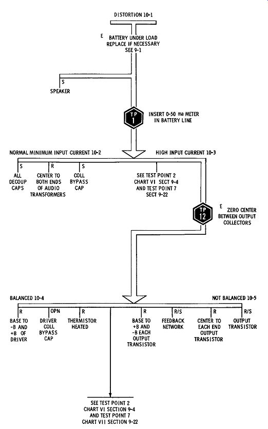
10-1
The first step in servicing any battery-powered equipment is to check the battery voltage under load. This test should especially be made in a transistor receiver which has distortion.
The speaker should be the next unit checked as soon as proper battery voltage is established. The best check is to substitute a good one, but when the original speaker has an odd value of voice-coil resistance this may not be possible. Using a speaker which does not match may produce as much distortion as the defective speaker. A careful visual check of the speaker may reveal a fault.
The next step is the same TEST POINT 1 which was used to begin each analysis in Section 9. If it can be determined that the minimum input current (with the volume control at minimum) is normal as specified in the schematic, then the testing is confined to only a few possibilities.
10-2
Electrolytic capacitors in decoupling networks are the most likely suspects, and from the normal input current reading it can be safely assumed that a defective one will be open and not shorted. Bridging across the capacitors with a unit known to be good is an easy method of checking them. Many technicians clip a pair of leads having needle-pointed probes to the test capacitor which can then be used conveniently on the printed-circuit board. Fig. 10-1 shows C1, C4, and C16 as the electrolytics in decoupling networks.
In addition to the electrolytics, the circuit in Fig. 10-1 employs a number of 10,000-mmf (that is, 0.01-mfd) capacitors in decoupling and bypass circuits. These are C7, CSA and B, C10, C11, C14, and Cl5. These can all be checked by bridging them with a capacitor known to be good.
It is not necessary to check electrolytics C2 or C3 when the input current is normal, because if either of these units is shorted, the collector current of transistor X4 will increase.
If the capacitors are open, there will be no sound in the case of C2 and low volume in the case of C3.
The input and output transformers in the push-pull output stage are a common cause of distortion because they usually fail in a way which causes them to have unequal resistances between the center and the end. The chart therefore recommends that the ohmmeter be applied from the center to each end so that the resistances can be compared.
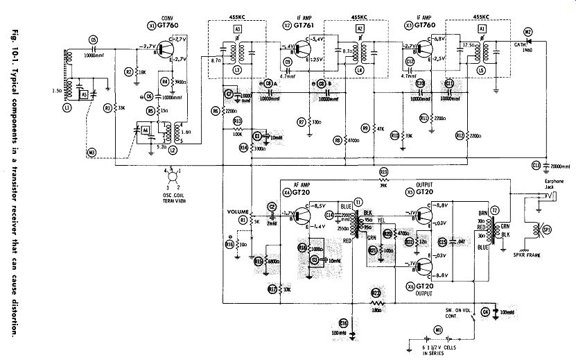
Fig. 10-1
TEST POINT 12, CHART IX HIGH INPUT CURRENT
10-3
The high input current is caused by excessive collector current through a transistor, or by some leaky component (such as C14 in Fig. 10-1) connected from +B to -B with low resistance in series. Parts which are connected like C14 cause high input current when they are leaky, but they do not cause distortion. This is because the current drawn by their failure does not carry any signal and does not pass through any amplifier. A leakage through Cl4, for example, would be wasted bleeder current drawn from the battery. As long as this current does not become large enough to reduce the battery voltage, it will have no effect on the operation of the receiver, except to shorten the life of the battery.
Therefore, when distortion is the symptom and the input current is high, all components whose leakage current would not pass through a transistor can be eliminated as suspects.
When the offending stage is identified, tests can be performed to decide whether the transistor is defective or the bias circuit has failed in a way which puts high forward bias on the base. After finding high input current, the testing can move directly to TEST POINT 2 in SERVICING CHART VII, described in Section 9-4, or to TEST POINT 7 (in the same chart) which is described in Section 9-22, because these tests lead to components whose leakage affects the current through transistors. However, since it is most often the output transistors which cause distortion, TEST POINT 12 can be used to analyze the output stages first.
TEST POINT 12, CHART IX USING A ZERO-CENTERED VTVM TO FIND A FAULTY OUTPUT TRANSISTOR
Fig. 10-2 illustrates the use of a zero-centered VTVM to identify the output transistor that is causing distortion. The
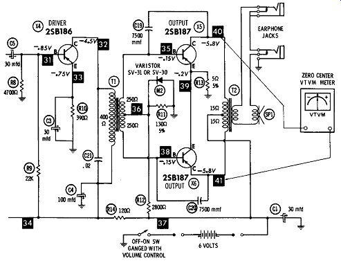
Fig. 10-2. Using a zero-centered VTVM to detect a faulty output transistor.
schematic shows that there should be equal voltages from each collector to ground when there is no incoming signal. Thus, the VTVM will not be deflected in either direction. But if one of the transistors has excessive collector current its collector voltage will be lower (more positive) than the collector voltage of the other transistor, and this will cause the meter to he deflected. The deflection will be toward the positive end of the scale when the positive probe is on the defective transistor, and toward the negative end when the negative probe is on the defective transistor.
With a considerable amount of unbalance in the output circuit, the voltage between the collectors will still be less than 1 volt. Excessive deflection which pins the needle on the 1-volt scale indicates that one transistor is open. In this case, its collector voltage will be greater (more negative), and the indications described in the preceding paragraph will be reversed.
The technician should expect some slight unbalance, even with well-matched transistors which are working properly, because of the unbalance in the transformer resistance, but this will be in the order of 0.1 or 0.2 volt. Obviously, this test is useful only when the output transistors are connected in push-pull and use a center-tapped output transformer.
Further Tests When the Voltage Is Balanced
10-4
A balanced voltage seems to eliminate the output transistors as the cause of distortion. Only three simple tests need to be made to establish this with certainty:
1. Resistance measurement from the base to +B and -B in both output transistors, as well as the audio driver.
2. Open one end of the collector bypass capacitor, and check for distorted sound.
3. Resistance measurement of the thermistor or varistor.
The collector bypass capacitor (C15 in Fig. 10-1) does not need to be checked for distortion unless there is also motor boating. The varistor, shown in Fig. 10-2 as M2, is a tempera ture-sensitive device that changes its resistance as the temperature of the transistors increases. It must be checked when it is cold and also when it is hot. This can be done easily by bringing the soldering gun near the unit while measuring the resistance. The two values of resistance will be given in the parts list, but this referral is not necessary, since, if the resistance changes at all, it is very likely that the unit is functioning properly.
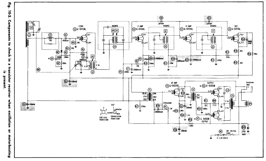
Fig. 10-3
When the preceding checks are completed, the technician should move to Sections 9-4 and 9-22, as shown in the chart.
Further Tests When the Collector Voltages Are Not Balanced
10-5
If the collector voltages are not equal it is certain that the output stage is responsible for the distortion, and it only remains to locate the exact component causing the fault. Four possibilities are indicated on the chart, but individual circuits differ in the "extras" which may be included, and the technician must leave no part unchecked. A comparison between the output stages of Figs. 10-1 and 10-2 will indicate a number of differences which would not be apparent from looking at the two chassis without the schematics. Note, in particular, capacitors C19 and C20 in Fig. 10-2. These permit feedback to stabilize the amplifier at high frequencies. It is easy to see how leakage in either one would cause unbalanced collector voltages.
OSCILLATION OR MOTORBOATING
Again it is important to make sure of the condition of the battery-never assume it to be good, even if it is new. Next, in order to get a clue as to which section of the receiver is at fault, the tuning capacitor is rotated through its range. If this affects oscillation, it is likely that one or more of the stages between the antenna and the detector are involved.
10-7
The first step is to perform a complete IF alignment according to the instructions given in the schematic. In some models, the IF transformers are sealed with wax, making it difficult to reach the tuning slugs. These transformers can be aligned easily if a small metal screwdriver is heated and then pushed down through the wax. After the slug is adjusted, the wax can be resealed with the soldering gun.
There is a double reason for going through the alignment procedure first: (1) it gives assurance that the stages are aligned properly; (2) it may reveal the defective stage because the signal cannot be peaked properly with the IF -transformer adjustment.
The circuit in Fig. 10-3 has neutralizing capacitors, CS and C11, in the IF stages. These are a common cause of oscillation, but not always because the capacitors themselves have failed.
Instead, it is because the internal capacity of one of the transistors has changed, and a different amount of capacity is needed to neutralize the stage.
Each of the electrolytic capacitors, C1, C2, C3, C15, and C16, should be bridged with a good unit of sufficient capacity. As in the case of distortion, it is very unlikely that one of these capacitors is shorted, so it is not necessary to remove them from the circuit before testing. The bypass capacitors in the IF and detector stages should also be bridged using a .05-mfd unit.
One precaution should be given in connection with these electrolytics. These capacitors often fail because one of the leads comes unsoldered inside the unit, giving the impression of an intermittent in the printed-circuit board. The fault may respond to resoldering the lead at the board because the lead is sometimes heated enough to resolder it temporarily, but it will undoubtedly break loose again. It is better to replace the electrolytic involved, even when the trouble seems to be in the printed board.
Further Tests When the Oscillation Is Not Affected by Tuning
10-8
This points to a failure in the audio section, and TEST POINT 13 is used to separate the audio output from the driver stage.
TEST POINT 13, CHART X TURN THE VOLUME CONTROL TO MINIMUM
10-9
If changing the setting of the volume control to a minimum changes the oscillation, this suggests that the volume control and base of the driver stage are both part of the oscillatory path. Besides the detector diode and the AVC filter, which should be suspected at once, the chart suggests testing decoupling filters such as C14, Cl5, C16, and C3 in Fig. 10-3.
The feedback network in this circuit does not return to the base of the driver stage, so it does not need to be checked in this case.
Further Tests When the Oscillation Remains the Same
10-10
This definitely limits the testing to the audio stages following the one which contains the volume control. The collector bypass capacitor C17 should be bridged first, followed by a check of the resistances from the center to either end of the input transformer. If none of these is the cause of oscillation, it may be assumed that one of the output transistors is at fault. This fault can be found by shorting the base to the emitter in each of the push-pull transistors. The one which causes the oscillation to stop when the base is shorted to the emitter is probably the defective unit.
CHART XI LOW GAIN
10-11
As in every symptom, the testing starts with a check of the battery. Then the milliammeter is inserted in the battery line to measure the input current, which is checked against the value given in the schematic.
10-12
Only the minimum value of the input current is useful now, because there is probably not enough signal to draw the rated current at normal volume. When the minimum input current is correct, a complete alignment is called for in the case of low gain. The manufacturer's instructions should be followed as closely as possible. The antenna should be inspected carefully at this time. Leads are often broken while changing batteries.
If all the adjustments seem to go well, but the receiver does not track properly in the middle of the broadcast band, the tuning capacitor itself may be at fault. It is unusual to suspect the tuning capacitor when signals can be tuned in, but in transistor receivers, failure of the tuning capacitor is a common fault. A cause of low gain that does not have much effect on input current is leakage through the auxiliary A VC diode. This should be checked early in the analysis. (See Section 9-24 and diode M2 in Fig. 10-3.) Disconnecting the diode will restore normal gain if it is defective.
Further Tests When Input Current Is Not Correct
10-15
It is common for a transistor to be the cause of low gain, and this usually is accompanied by a change in the input current. There is one exception, however, and this concerns the emitter bypass capacitors. If one of these is open, the result is increased input resistance to the stage and, consequently, a decrease in output. To test for this, simply bridge a good unit across each of the emitter bypass capacitors.
A shorted capacitor in the emitter of a stage can also reduce the gain by increasing the forward bias to the point where the collector is saturated, and incoming signals cannot produce a change in collector current. So, in the case of low gain, it is important to check all the emitter bypass capacitors very care fully.
A common cause of low gain is the AVC filter. Leakage here reduces the negative voltage on the base of the controlled stage, which reduces the output voltage of the stage.
The chart finally refers to Section 9-3 if the input current is high, and to Section 9-25 if it is low. Analysis in these sections will serve to locate the cause of low gain.
-------- Servicing Chart IX: Distortion.
Servicing Chart X: Oscillation or Motorboating.
Servicing Chart XI: Low Gain.
QUIZ
1. What precaution should always be taken when checking a battery?
2. When it appears that the printed circuit is intermittent in connection with an electrolytic capacitor, what is likely to be wrong, and what action is recommended?
3. Describe the symptom and the preliminary tests which should be used before the zero-centered voltmeter is applied to the collectors of the output transistors.
4. Suppose the complaint is that the sound is distorted, and the batteries seem to wear out faster than they did when the radio was new.
a. Refer to Fig. 10-1 and list the first five steps that you would take.
b. If the receiver has an output stage like that of Fig. 10-2, what part not mentioned above might you also suspect?
5. Describe the three tests used to isolate the cause of oscillation to a definite section of the receiver.
6. In Fig. 10-3, suppose R13 is open.
a. Describe all the changes in voltages and currents that would occur.
b. What would be the symptom in the sound, and what would be the result of each of the steps taken according to the chart at the end of this section?
7. The receiver in Fig. 10-3 has severe distortion. The following tests have been made :
a. Battery current is normal at minimum volume.
b. All decoupling and bypass capacitors have been checked.
c. Both audio transformers are OK.
d. Voltage analysis reveals that the emitter voltage of X5 is 3 volts positive, the base voltage is normal, and the collector voltage is 1.25.
What part would you suspect, and what would be your next test?
8. With what symptom in the sound and after what tests would you recommend complete alignment?
9. List all the ways that the battery can be responsible for symptoms mentioned in this section and in Section 9.
State the symptom and the tests which identify the battery in each case.
10. Look up the schematic of a receiver which has some feature not mentioned in this section which could cause distortion. Draw a partial schematic of the circuits involved, and explain how distortion might be caused.