The charts at the end of this section are more complex than those used previously, because, in transistorized receivers, the symptoms may overlap and some of the tests appear in more than one of the charts. In addition, the stages are complicated by the bias network, which is always necessary and requires extra testing. It is often important to consider current measurements which are not usually necessary in servicing vacuum tube equipment.
Besides the electronic differences, servicing transistor receivers is complicated by the compactness of the printed-circuit board and the difficulty in identifying transistor leads and other components. The schematic and technical data are some times unavailable, and replacement parts cannot be obtained because the original part cannot be identified. It is extremely difficult to locate test points in the circuits and make measurements on a printed-circuit board without schematic data.
Despite the difficulties involved, transistor radio servicing can be profitable to the technician who has the knowledge, skill, and tools to do the work efficiently. Expert workmen in all trades exhibit one characteristic in common-they possess specialized tools for their work, and they have a well-arranged place in which to work. Therefore, good advice to the beginning technician who considers transistor radio servicing is to obtain the special tools and equipment needed and arrange a place where the job can be "set up" and worked on properly.
This will include:
1. DC milliammeter with ranges from 0.1 ma up to 50 ma.
2. Needle-point probes and miniature clips.
3. A suitable power supply.
4. Tools for working on printed-circuit boards, including a razor blade mounted in a holder similar to the ones used in model building.
5. An audio signal source capable of injecting signals into low-impedance circuits.
6. An RF signal source.
7. A work space lighted from beneath through frosted glass to facilitate looking through semitransparent circuit boards which have printed wiring and components on both sides.
In connection with the preceding list, the importance of having a schematic and ·a pictorial view of the circuit board is emphasized. The beginning technician soon learns that without the technical data it is impossible to make profitable repairs on transistor radios. Many of these receivers are low-priced units, and the work must be done quickly in order to keep the repair costs commensurate with the value of the equipment.
It is embarrassing to present a bill which includes a charge for 4 or 5 hours of labor to replace a part whose value is only a few cents, and it is doubtful that the owner of the receiver would recommend the technician even if his radio was satisfactorily repaired. In most cases, repairs cannot be completed without the technical data; and even when they can be, there will be either little satisfaction to the customer or no profit to the technician. Follow the rule of refusing to take repair work which cannot be completed profitably.
SYMPTOM--NO SIGNALS
9-1
This condition often means a completely dead receiver.
But there are no tube filaments to observe, and one cannot tell by listening whether to suspect the power supply or some circuit such as the audio output stage. For this reason, the first step is to check the battery. The battery voltage should be measured while under load (with the receiver turned on), and if it is more than one volt below its rating, it should be replaced after repairs are completed. But during repairs, it is better to use an AC-powered supply which is metered.
TEST POINT 1, CHART VI MEASURE INPUT CURRENT
9-2
The symptom of No Signals occurs in one of three ways--with very low ( or zero) input current, with normal input current, or with very high input current. Since the testing procedures will be different for each of these conditions, the first test is to determine the input current by inserting a 0- to 50-ma meter in series with one battery lead. The ammeter on the ordinary battery eliminator will not respond to the small currents drawn by transistor equipment, so an extra meter will be needed. The correct currents at minimum and normal volume are always stated on the front of the Sams PHOTO FACT for that particular receiver. The rating at normal volume will be much higher than at minimum because of the increase in conduction of the class-B output stage which is practically cut off when there is no audio signal to drive it.
Fig. 9-1 illustrates the procedure thus far. The decision as to which chart to use as a guide is based on the amount of input current drawn by the receiver. Each of the charts will be discussed separately.
BATTERY UNDER LOAD. REPLACE IF NECESSARY SEE
9-1

Fig. 9-1. Initial testing procedure.
TEST POINT 2, CHART VI
SHORT BASE TO EMITIER IN EACH STAGE
9-3
Chart VI is for the condition of No Signals with higher than normal input current. Since this condition is most likely to result from shorted or leaking electrolytics in the battery decoupling networks, it is best to check these first. The leaky capacitor can be identified by the decrease in input current when it is disconnected. If all decoupling circuits seem to be functioning properly, and no parts are overheated by the excessive current, the testing proceeds with TEST POINT 2.
9-4
When the emitter is shorted to the base, zero bias is applied to the transistor base and, in this state, it is supposed to be cut off. If a large change in the input current results from shorting the base to the emitter of a particular stage, it is probably that stage which is responsible for the excessive current. Further, since a normal transistor cuts off when the bias is removed, it is clear that the defect is in the bias circuitry and not in the transistor itself.

Fig. 9-2. Test points in the output stage of a transistor receiver.
Tests When Input Current Decreases
9-5
In CHART VI under TEST POINT 2 are several suggested tests. Figs. 9-2, 9-3, and 9-4 show examples of the components mentioned. In Fig. 9-2, R13 and R14 are the bias resistors, and they should both be checked, especially R13, for if this resistance is open, the forward bias on the output transistor will be greater.
It is advisable to measure between points which are indicated on the schematic and on the pictorial drawing of the circuit board; such as between points ! 24 I and ~ to check the resistance of R13. Besides making it easier to locate the test points accurately, this practice also provides an additional check on the condition of the printed connections to the component being checked.
One precaution should be mentioned when using the ohm meter to check components which are connected to elements of a transistor. The transistor, unlike its vacuum-tube counter part, is activated by the voltage from the ohmmeter and thus becomes an active part of the circuits, even though the power supply to the receiver is disconnected. Fig. 9-5 shows how an erroneous reading could be obtained because of conduction through the emitter-base junction when the ohmmeter polarity puts forward bias on the transistor. An unsuspecting technician might conclude from the reading in part A of Fig. 9-5 that the bias resistor had changed value. Whenever the possibility of such an error exists, it is best to reverse the ohmmeter leads and repeat the measurement.
If C5 in Fig. 9-2 is partially shorted there will also be excessive negative voltage on the base of the output transistor, resulting in very heavy input current which will decrease when the base and emitter are shorted together. The voltage readings at the elements of the transistors in Fig. 9-2 may be confusing because they are stated as positive voltages relative to ground. Some schematics are drawn this way with the negative terminal of the battery grounded and the collectors of the PNP transistors returned to ground. Since all voltages are measured from chassis ground, the collector voltage on X3, for example, is 0.5 volt positive with respect to chassis ground. It is still a negative voltage with respect to the emitter line numbered 25 and 25 on the schematic, however.
Fig. 9-3 is drawn in the usual fashion, with the emitters grounded and the positive terminal of the battery grounded.
Note that the primary of transformer T1 is connected to -5. 7 volts, and that the secondary is connected to the bases of the output transistors. Leakage through the transformer could put nearly 5.7 volts negative on the bases of the output transistors and cause excessive current to be drawn by the stage. There probably would be no output signal because the saturated output transistors would be conducting simultaneously, and the input signal would be too small to have any effect on collector currents.
SERVICING CHART VI suggests checking the transformer by opening the battery end of the primary and rechecking the input current at TEST POINT 1.
The abbreviation, OPN, meaning to open the connection, is used in the chart for this test; this is the first time this symbol has been used in any of the Servicing Charts.

Fig. 9-3.
Other possible causes of excessive current in the AF and driver stages (X5 and X6 in Fig. 9-3) are the emitter bypass capacitors, C7 and C9. X6 is supposed to have -1.4 volts on its emitter and -1.7 volts on its base, thus placing -0.3 volt of forward bias on the base. If C9 is shorted, the emitter voltage will be zero, and the base voltage will remain nearly the same. This will result in about -1.7 volts of forward bias on the base and greatly increase the input current. If the base and emitter are shorted together, as in TEST POINT 2, the bias will disappear, and the input current will return to a reasonable value.

Fig. 9-4. Transistor receiver IF-amplifier section.
Fig. 9-4 shows two IF stages that could cause excessive input current due to increased forward bias. If the IF trans former L6 has a short from primary to secondary, the same condition will prevail, as noted in the case of T1 in Fig. 9-3.
Another cause is a shorted neutralizing capacitor, such as C21 in Fig. 9-4. This capacitor can easily be eliminated as a suspected faulty part by disconnecting one end of it and checking the input current.
When the transistor itself is the cause of excessive input current, it is unlikely that the current will be reduced by shorting the base to the emitter. The remote possibility does exist, however, that the gain of the transistor has greatly increased, or that a transistor having characteristics greatly different from the original has been used as a replacement.
In such a case, the transistor can be roughly tested with an ohmmeter in the following manner.

Fig. 9-5. An Ohmmeter can cause erroneous readings in a transistor circuit.
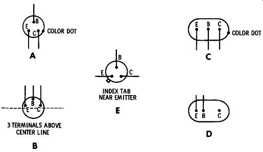
Fig. 9-6. Identification of transistor leads.
Remove the transistor from the circuit by disconnecting at least two leads, and examine the bottom to determine which lead is from each of the elements. Fig. 9-6 shows that the base lead is always in the middle, and that when two of the leads are closer together, they are the base and emitter. When the leads are evenly spaced, the collector is identified by a colored dot.
9-6
An ordinary ohmmeter on the R x 100 range will supply enough voltage and current for checking any low-power transistor. Table 9-1 lists the average resistances to be expected with the probes used in either polarity.

TABLE 9-1. Resistance Reading for Low-Power Transistors (use R X 100 range)

TABLE 9-2. Resistance Reading for High-Power Transistors (use R x 1 range)*
* In power transistors which have only two leads, the collector is connected to the outer shell.
The resistances given in the tables are only general guides; the actual value depends on the voltage applied across the junction and will be different with various makes of ohmmeters.
Also, some transistors fail only after they have been in use long enough to raise the temperature of the junctions. This is particularly true of the small power transistors commonly used in the push-pull output stages of receivers. The best way to check a transistor which has such a failure is to substitute one known to be good.
A different approach to using the ohmmeter is preferred by many technicians, although it is really not any more reliable than other methods. Begin by placing the probes across the emitter and collector leads. Reverse them until the polarity which gives the minimum resistance is found. Next, adjust the ohmmeter to the lowest scale which gives a nearly full scale deflection (minimum resistance). Now, when the probes are reversed, the meter should show about mid-scale deflection.
The larger the power capability of the transistor, the lower this second reading will be.
Further Tests When There Is No Change in the Input Current at TEST POINT 2
This indicates that the defect is either a component which does not affect the bias of a stage like those already described, or it is a transistor with a direct short from emitter to collector, which is not affected by removing the base bias in TEST POIN'I' 2. The next test will decide which condition exists.
TEST POINT 3, CHART VI OPEN THE EMITTER OF EACH STAGE
9-7, 9-8
If a stage can be found which causes the input current measured at TEST POINT 1 to decrease a considerable amount when the emitter is opened, it is obvious that the transistor in this stage is defective, since its current did not change when the base was shorted to the emitter in TEST POINT 2.
The transistor can be checked with the ohmmeter after it is removed. The voltage between the base terminal in the circuit and ground should be checked against the value given in the schematic to make sure that the new transistor will not be ruined. The voltage will be fairly accurate even when it is measured with the transistor removed. The resistance from the emitter terminal to the + battery line should also be checked.
Further Tests When There Is No Change in the Input Current With Emitters Opened
9-9
This indicates that the defect is not a transistor. A voltage reading at each collector is recommended in the chart because a low voltage at one of these may lead to the discovery of a shorted capacitor such as C5, C7, C6, C15, or tuning capacitor A5, in Fig. 9-7. When the voltage is absent at a collector, the meter is moved across the next component in series toward the battery, and a new measurement is taken. For example, in Fig. 9-7, suppose CS is shorted. There will be no voltage at the collector of X1. The next reading should be taken from terminal 2 of L2 to ground, where there should still be no voltage. A reading at terminal 1 will also show no voltage. The meter should now be moved to the battery side of R5 where 3 or 4 volts will be present, indicating that the meter has just been moved past the defective component.

Fig. 9-7. RF amplifier, mixer, and oscillator section of a typical transistor
receiver.
In a circuit like the one shown in Fig. 9-8, a high reading indicates trouble. Other components which could cause the input current to be high are listed on the right under TEST POINT 3 in SERVICING CHART VI.
CHART VII NO SIGNALS, NORMAL INPUT CURRENT
9-10
When the input current checks normal, the procedure for the symptom of No Signals follows the pattern of SER VICING CHART VII. It is probable that the current reading will be the minimum value because, with no signals, the output stage will not be driven into high conduction. There is an exception, however. If the speaker has failed and the output stages are functioning normally, then the input current may be up to the value given in the schematic for normal volume. If the speaker is suspected, it can be checked at once by using the ohmmeter test described in Section 3-12.

Fig. 9-8. Collector returned to common ground.

TEST POINT 4, CHART VII
INJECT AUDIO AT VOLUME CONTROL
9-11
When the input current is at the minimum specified in the schematic, there is no way of knowing whether the audio stages have actually failed and are not drawing their share of current from the battery, or whether there is no signal to drive the audio stages and cause them to conduct. TEST POINT 4, injection of audio at the volume control, is a familiar operation from the study of vacuum-tube radios, and it is done here for the same reason. The technician must keep in mind that the input impedance may be quite low, and the finger or the tip of the soldering gun might not provide enough signal to produce much output. The signal injection should be done with care because the rest of the analysis will be based on the results of whether or not the audio stages will amplify.
Further Tests When No Sound Results From TEST POINT 4
9-12
Once the conclusion has been reached that the audio section has failed, a number of preliminary tests should be made immediately. These are shown in SERVICING CHART VII under TEST POINT 4, and all are associated with the audio output stage. Injection of a signal directly into the output transistors is not a reliable test, nor are the other tests that were used with tube-type receivers.
Only one of the tests requires explanation-the measurement of AC voltage across the primary of the audio input transformer (see Fig. 9-9). This should be done with the volume control turned to maximum and while the station selector is turned through its range. An alternative method is to inject audio from a signal generator at the volume control.
If any signal appears in the transformer, the AC voltmeter will respond-about 3 to 5 volts AC can be expected. If there is no voltage indicated with collector voltage on the audio driver transistor, there is still the possibility that bypass capacitor C19 is shorted. The suggestion in the chart is to open one end of this capacitor and look for the AC signal, but if the transformer resistance is given, the ohmmeter can be used without disconnecting Cl9.
(A) Partial schematic. (B) Printed board showing test points.

Fig. 9-9. Typical transistor receiver.
TEST POINT 5, CHART VII NO SIGNAL OUTPUT FROM THE DRIVER
9-13
With no output from the driver stage, this test is used to decide whether the defect is in the transistor or in the circuitry of the input or output of the stage. With the DC voltmeter between the collector and emitter, points 44 and 45 in Fig. 9-10, for example, the base is shorted to the emitter, thus removing all bias. One of three results must occur:
1. The normal voltage (3.1 volts in Fig. 9-10) will rise to the full battery voltage. It is important to note that the Vee will not be 4.5 volts, as given at the collector in the schematic, because V,. is the difference between the emitter and collector voltages.
2. Vce will be missing.
3. Vce will be incorrect, or it will not change correctly.

Fig. 9-10. Circuit showing application of TEST POINT 5, CHART VII.
9-14
In the first case, the response is entirely normal, and the driver transistor as well as its bias network, R22 and R23, and output circuit C23 and T1 must all be operating properly.
Obviously, the defect must be present in the coupling through CS to the preceding stage. An ohmmeter can be used to examine the components here. The chart also mentions the collector bypass capacitor, C23, as a possibility, but this is unlikely when Yee is normal before shorting the base and emitter. It is mentioned only because its leakage could reduce the load resistance in the collector but slightly, resulting in inconclusive readings at TEST POINT 5.
9-15
When the second result listed occurs, it is clear that either the collector or the emitter lead to the battery is open because of an open in the printed wiring, a defective part in series, or a shorted transistor. It is difficult to establish a rule for the amount of change in input current to expect at TEST POINT 1 when a low-power transistor is shorted. The current drawn by a shorted audio-driver transistor may not register on the milliammeter because, simultaneously, the current in the class-B output transistors drops to a low value due to no in coming signal to drive them. The output transistors may ac count for a large part of the normal current stated in the technical data for the receiver.
In circuits like the one in Fig. 9-9, where there is still a total resistance in the emitter-collector circuit of 1490 ohms, even with a shorted transistor, the maximum current that could be drawn by the stage is only:
6 volts 1490 ohms = 4.02 ma
From the 0.8 volt on the emitter, it can be determined that normal no-signal emitter-collector current is 0.8 ma (taking lb as negligible with no signal), and it would not be unreason able to expect peaks of 1 or 2 ma with a signal applied. So it can be seen that a shorted driver might not increase the input current at TEST POINT 1 by more than a milliamp or so.
The best way to proceed when Vee is missing is to remove the transistor from the circuit by slashing the emitter and collector leads with a razor blade and measure the voltage again. If full battery voltage appears, the transistor was bad.
If the voltage does not appear, some component in series with the battery, or the leads themselves, may be open.
A confusing situation can arise in circuits which use a large emitter resistance, like the driver stage shown in Fig. 9-9.
The purpose of the emitter resistor is to increase the stability by establishing -0.8 volt of emitter voltage. This voltage, when applied in conjunction with -1 volt of base voltage formed by the divider R12 and R13, produces the net forward bias of -0.2 volt. Keeping in mind that the emitter voltage is produced as a result of current which flows in the collector circuit, one can see that if the collector were open-circuited (by an open transformer primary, for instance), there would be practically no emitter voltage.
The base voltage, however, would not change much under these conditions because it is the drop across R12 and is determined by the proportions in the voltage divider. Now, if the emitter voltage is reduced to almost zero and the base voltage remains nearly -1 volt, the base-emitter voltage will become almost -1 volt. The resulting increase in base current may ruin the transistor, and may also ruin subsequent replacements which are installed without first checking to see if the collector circuit is open.
9-16
The third possible result of TEST POINT 5 is that Vee does not change properly, or that it is not correct to start with. The parts to be checked are shown on the chart.
One of the tests suggests an ohmmeter check of the bias network. A new abbreviation is used on the chart at this point, where the negative terminal of the battery is referred to as - B and the positive terminal as + B. Since so many other things about transistors are backwards as compared to conventional vacuum-tube circuits, it seems justifiable to reverse the usual symbols of B- and B+ because there are no B+ or B- power-supply terminals in the sense that they are used with vacuum tubes.
TEST POINT 6, CHART VII AUDIO SECTION WORKING PROPERLY
9-17
Referring to SERVICING CHART VII under TEST POINT 4, the procedure shown is to be followed when it is found that the defect is in the RF or IF sections. TEST POINT 6 calls for a check on the operation of the oscillator section, and there are several ways that this can be done. The choice will depend on the accessibility of terminals for testing on the individual chassis. A method which works on most receivers is to measure the AC voltage across the oscillator tuning capacitor, or across the oscillator tank. If a good VTVM is used, oscillator operation will be determined by a small AC voltage generated. Another way is to use an oscilloscope across either of the above points.
A method recommended by some experts is to bring the suspected chassis near another operating receiver which is tuned to a weak station, and rotate the tuning dial on the receiver being tested. If a beat can be obtained at some point on the tuning, this is due to radiation from the oscillator in the receiver undergoing repairs and is evidence of oscillation.
A favorite method of many technicians is to measure the DC bias between the base and emitter of the oscillator transistor while the tuning dial is rotated through its range. There should be a DC voltage present, of course, even if the oscillator is not functioning, but when it is operating, the DC bias will fluctuate as the tuning capacitor is rotated. Sometimes when oscillations are strong, a positive voltage will be found on the base which disappears with a touch of the finger, like grid-leak bias.
The determination of oscillator operation in transistor receivers is a tricky test procedure, and the results of any of the tests described should be considered as indications only, not as conclusive proof. It will soon become apparent if an error has been made, and the technician should then retrace his steps.
Further Tests When It Appears That the Oscillator Has Failed
9-18
The components to be suspected will depend on whether the oscillator stage still has a fixed forward bias, or whether the defect has removed all forward bias. Two typical oscillator-mixer stages are shown in Figs. 9-8 and 9-11, in which loss of bias might be caused by different components. The test results will be different in each circuit because of +B ground in Fig. 9-11 compared to -B ground in Fig. 9-8.
9-19
In Fig. 9-8, the fixed DC bias is 0.1 volt and, if this is missing, the first test suggested on the chart is to use an ohm meter from the base to ground and from the base to + B. The condition of R2 and R3 can thus be determined if the precautions mentioned in Section 9-5 regarding polarity of the ohm meter are observed. The missing bias could be the result of a shorted tuning capacitor, A5, or a shorted capacitor, C6. The chart also suggests measuring the resistance from the emitter to + B, which will indicate the condition of R4. The resistance from the emitter to ground should also be measured in this circuit. The condition of the transistor itself should not be overlooked, and it too can be checked with the ohmmeter or by substitution.

Fig. 9-11. Circuit showing application of TEST POINT 6, CHART VII.
If the bias in the circuit of Fig. 9-11 is missing, a somewhat different procedure should be followed. The tuning capacitor will not be suspected, but a shorted C9 will probably remove the forward bias. It is not necessary to check the resistance from the emitter to -B.
9-20
When the DC forward bias voltage is present, a different approach is taken to the problem. Referring again to Fig. 9-8, nothing in the emitter or base circuits is suspected, because all these parts must be good to produce the forward bias. Tests should begin with the collector voltage and tracing through test terminals CT} , I]) , and m:) if it is missing. The oscillator tuning capacitor, A4, and blocking capacitor C7 should not be overlooked as a trouble source if the collector voltage seems normal.
In the circuit in Fig. 9-11, a normal bias of 0.2 volt does not exclude the tuning capacitors A5 and A4 from suspicion. But it seems unnecessary to check C9 or C11 for shorts, although an open C9, or the printed leads thereto, would stop oscillation without removing the DC bias.

Fig. 9-12. Increasing forward bias.
The oscillator coil in both circuits is a good suspect and the soldering at the terminals should be checked. It is a good idea to resolder all of the connections around the oscillator components if DC bias is present but the oscillator is not running.
9-21
The transistor itself is a common cause of oscillator failure and an interesting test is suggested in the chart. The forward bias is purposely increased while measuring the voltage between the emitter and + B. Fig. 9-12 shows the method to use. A 100K potentiometer is connected from the negative battery terminal to the base, and a small resistor is used in series with the center tap to prevent shorting the base directly to - B. Begin with maximum resistance, and carefully reduce the resistance to increase the bias. The transistor should begin to conduct more, and the voltage drop across the emitter resistor should increase. For low-power transistors with an emitter resistance of 1000 ohms or less, ½ to 1 volt should be considered a significant increase.
If the voltage increases, the transistor is probably behaving normally, and the reason for oscillator failure is a defect in the feedback circuit. If the emitter voltage does not increase when the forward bias is increased, and proper collector voltage is present, it is very likely that the transistor will need replacement.
TEST POINT 7, CHART VII IF OSCILLATOR IS RUNNING, MEASURE V_ce IN RF AND IF STAGES
9-22
TEST POINT 7 is used to determine which IF or RF stage has failed when there are no signals and the oscillator is running. The antenna coils and tuning capacitors should be checked with the ohmmeter first.
A signal generator could be used to inject signals starting at the detector and moving progressively toward the antenna, but using a signal generator in transistorized IF stages re quires considerable experience to avoid the confusion resulting from the signals feeding through a dead stage. It is easier and much more reliable to measure V ce in each RF and IF stage.
A defective stage will always exhibit incorrect Vce. When Vce is normal throughout, it is easy to check the few components whose failure could cause the No-Signal condition without affecting any Vce. Further Tests When Vee Is Found To Be Incorrect 9-23 Four suggestions are given in the chart, but the choice of which one to use will depend on the convenience of test terminals on the chassis, and whether Vee is too high or too low. To illustrate, we shall take a hypothetical case history and compare the test results in the two circuits of Fig. 9-13 and 9-14.

Fig. 9-13

Fig. 9-14. Circuit showing application of TEST POINT 7, CHART VII.
Suppose the receiver in Fig. 9-13 has a No-Signal condition, and the input current is not excessive, although it cannot be reduced to the minimum given on the schematic when the volume control is turned down. Therefore, the current is tentatively assumed to be normal. An injection of audio at the volume control produces normal sound, and it is noted that the input current rises when a signal is present, indicating that the output stages are operating normally.
Correct DC bias in the oscillator is found between points [3] and [D] , and it varies slightly when the tuning capacitor is rotated through its range. Also, 0.8 volt AC can be measured across the oscillator tuning capacitor; so it is assumed that the oscillator is operating and that the failure must be in the RF, IF, or detector circuit, or in the coupling between the detector and the audio.
Next the voltmeter is used to measure all Vce's in the RF and IF stages. This reveals a very low voltage in the second IF stage, indicating that the stage is conducting very heavy collector current or that a component in series with the collector supply line has failed, reducing the voltage available for the stage. All other Vce's are normal.
If it were shorted, the emitter bypass capacitor could increase the bias by removing the emitter voltage; but when C12 is opened there is no change. R7 checks correctly also.
C2 and C8 are not suspected, since these units could not increase the forward bias.
The ohmmeter is applied between the base and - B, and the base and + B, test points 16 to 10, and 16 to ground.
The precautions mentioned in Section 9-5 regarding the possibility of incorrect readings obtained in circuits were a transistor junction is connected, should be observed.
The reading from 16 to -B with the positive probe on 16! should be about 68K. In this instance, however, it reads 1000 ohms with the probes in either direction. The low reading in one direction is expected, but a low reading in both directions indicates either a defective transistor or trouble in the bias circuit. The next test is to cut the printed wiring leading to one end of R13, removing the resistor completely from the circuit. When this is done, the resistor reads 68K on the ohm meter.
Two tests of the transistor itself are mentioned in the chart.
The ohmmeter check seems most appropriate, since it is al ready known that the transistor is conducting heavy collector current. The application of additional forward bias is used when unusually high V"" indicates that the transistor may be cut off. After two of the leads are cut to remove the transistor from the circuit, it is checked with an ohmmeter according to the method described in Section 9-6, and it responds normally in every way. With the transistor still out of the circuit, the resistance from the base lead to - B is checked again, and it is still about 1000 ohms. It is clear now that there is a shorted component between the base of the transistor and - B. Only two possibilities remain--leakage from primary to secondary in L4, or leakage through the neutralizing capacitor, C11. By making a slice with a razor blade to open the printed w1rmg at some convenient place, such as between terminal 19 and C11, the fault will be located. When this is done, Vee rises and a replacement of C11 restores normal operation. If Vee did not rise to normal, extensive tests of the transformer and the AGC line would have to be made.
A defective transformer is identified by the procedure de scribed in Section 5-11, taking note of the opposite polarity used with PNP transistors. IF transformers often fail in transistor radios, and many such receivers are not repaired be cause the technician does not carry his analysis far enough to find the defective unit (see Fig. 9-15).

Fig. 9-15. Checking IF transformer for leakage.
A different series of tests will result from the same failure in the circuit of Fig. 9-14. This receiver includes an RF amplifier stage, and Vee on this stage as well as the others must be checked. Assuming the same fault (about 1000-ohms leakage through neutralizing capacitors C18 in the second IF stage), the same series of preliminary tests should be followed until the missing Vee is located in the second IF stage.
It should be noted in this circuit that part of the bias net work is R11, the emitter resistor of the first IF stage. The bias voltage is taken from the emitter resistor of the first IF stage, and thus it depends on the proper conduction of current in this transistor. If the neutralizing capacitor C18 were shorted, additional current would flow through R11, making the emitter of the first IF stage more negative. This would certainly cut off the transistor, but Vee would not rise to the full battery voltage, as it usually does when the transistor is cut off, be- cause of the voltage-divider action shown in Fig. 9-15. The technician must be aware of the differences in circuitry which cause exceptions to the usual rules. With incorrect Vee on two stages, one should immediately look for some component which is common to both stages, rather than tracing individual sections of each stage.
In other cases when the Vee is found to be very high when making the test at TEST POINT 7, this may be due to shorted decoupling capacitors, such as C2 or CS in Fig. 9-13. It could also be the result of an open connection from a base to - B through a defective resistor such as R9 in Fig. 9-14. High Vee can also be the result of an open collector or emitter element in the transistor. This possibility should not be over looked, especially if there has been much soldering done at the transistor lead connections. The leads are easily disconnected from the transistor elements at the junction inside by excessive heat applied to the leads.
Further Tests When All Vce's Are Normal
9-24
Normal Vee on all stages means that no stage is cut off or saturated with excessive collector current, and the defect is not in any transistor or base-bias circuit. Five possibilities are listed in CHART VII below TEST POINT 7. A study of Figs. 9-13 and 9-14 will reveal how these parts could produce the symptom of No Signals with the oscillator running and normal Vee throughout.
The emitter bypass capacitor is mentioned in the list, al though it is rather an exception. It actually will increase collector current if it is shorted but, when the voltmeter is placed between collector and emitter, the voltage may still be high enough to be mistaken for normal. This is because in IF and mixer stages there may be very little resistance in series with the collector to drop the voltage on the negative side of the transistor, and the emitter will be connected directly to + B through the shorted capacitor. This results in most of the battery voltage still appearing across the emitter-collector junction.
TEST POINT 8, CHART VIII NO SIGNALS, LOW INPUT CURRENT
The foregoing discussions have dealt with the symptom of No Signals when the input current is high and als9 when it is normal. CHART VIII is concerned with the condition of No Signals when the input current is less than the minimum specified in the schematic. This can be due to one of three causes:
1. A weak battery.
2. A increase in the value of a resistor in the battery decoupling network.
3. A defect in one of the stages which prevents the collector from drawing normal current.
9-25
A check of the battery is mentioned first in all the charts, and no further testing should ever be done until it is certain that the battery is in good condition, or unless the receiver has been connected to a battery eliminator. Then, if the input current is found to be more than 10 % below the minimum, TEST POINT 8 calls for a measurement of the collector-to-emitter voltage on each stage. If Vee is low on all the stages, it is probable that the defect will be found in the battery decoupling network. Most likely it will be the resistor that has failed because the capacitors will cause increased in put current if they are leaking.
Further Tests When One Vce Is Low
CHART VIII mentions a resistance check of the decoupling networks immediately under the heading Low or Missing, and this test should be made whenever all the Vce's are affected.
If only one stage shows low or missing Vee, then the defect is obviously confined to the emitter or collector circuit of that stage. The base-bias circuit would not be suspected with low input current, because bias failures which reduce Vee always do so by increasing the collector current.
Transistor failures usually involve shorted junctions which cause excessive current, or open junctions which cause a high Vce. Since both Vee and the input current are low, it is not likely that a transistor is defective.
Further Tests When One V_ce Is High
9-26
With low input current, and no failure in a decoupling network, it is common to find Vee very high in one stage. This means that the stage is not conducting and is therefore the cause of the No Signal, Low Input Current symptom. Of the three checks shown on the chart, the resistance measurement from the base to + B and to - B is the easiest to make, and will identify a failure in the bias network. Some technicians prefer to measure the base-to-emitter voltage as a check on the bias network, but it seems easier to measure relatively large resistances than to measure voltages that are in the order of tenths of a volt.
The application of forward bias, as described in Section 9-21, is another way to decide whether the transistor or some other component in the stage has failed. If the Yee drops when forward bias is applied to the transistor, the defect is probably in a bias network component, not the transistor itself.
A rough check on the transistor can be made according to the procedure described in Section 9-6, but the final proof that a transistor is bad is often the substitution of a new unit.
TEST POINT 9, CHART VIII WHEN V_ce IS NORMAL ON ALL STAGES
9-27
When no information can be gained from a check of Vce’s, it is necessary to use another approach to isolate the trouble to a particular section of the receiver. If the injection of audio at the volume control produces sound in the speaker and causes the input current to increase to normal, then it can safely be assumed that the problem is in the front end of the receiver and probably related to a tuned circuit. Defects such as those discussed in Section 9-17 should be suspected.
TEST POINT 10, CHART VIII APPLICATION OF FORWARD BIAS TO THE OUTPUT STAGE
9-28
If the injection of audio does not result in sound from the speaker along with an increase in input current, then it is clear that the trouble is in an audio stage. The method described for TEST POINT 5 in Section 9-12 can be used from this point on, or alternatively, TEST POINT 10 can be used to isolate the defective part into either the output stage or the audio driver. The method for applying forward bias was de scribed in Section 9-21.
Further Tests When Forward Bias Does Not Change Input Current This definitely indicates a failure in the output stage. With normal Yee there are only three possibilities.
1. High resistance in the collector circuit due to a defective output transformer ( or speaker when no output trans former is used) .
2. High resistance in the emitter circuit.
3. Defective transistor.
The ohmmeter is the instrument recommended in the chart to complete the isolation of the failure to one of the three places mentioned.
Fig. 9-16. Circuit showing application of TEST POINT 11, CHART VIII.
TEST POINT 11, CHART VIII FORWARD BIAS CAUSES AN INCREASE IN INPUT CURRENT
9-29
The output stage is probably working normally, but there is no input signal to drive the class-B transistors into conduction.
TEST POINT 11 calls for the use of an AC volt meter to determine the presence of an audio signal at the primary of the driver transformer. In using this method, it is a good idea to supply an audio signal at the volume control.
In Fig. 9-16 the AC voltmeter is applied between points 19 and @] . If there is an AC signal present, the parts listed under TEST POINT 11 should be checked. It is necessary to check only a few parts in the driver circuit because the determination of normal Vee at TEST POINT 8 eliminates most of the components.
Capacitor C15 is not mentioned on SERVICING CHART VIII because it does not appear in every circuit, but this part must also be checked when it is present. One end of the capacitor must be disconnected and the AC voltage measurement repeated. The capacitor cannot be checked with an ohmmeter while connected in the circuit because of the coil across it.
Further Tests When an AC Signal Is Found on the Driver Primary


9-30
This condition, combined with a normal Vee and a normal response to applied forward bias at TEST POINT 10, limits the fault to a few parts in the output stage. These are also shown in Fig. 9-16. The resistance from the emitters to + B should be checked. A greatly increased resistance at R15 still leaves a normal V_ce, even when there is no driving signal, but will prevent the transistors from conducting when audio appears at the secondary of the input transformer. R12, R13, and R14 are suspects, as well as the transformer secondary itself. C16 should be disconnected and the resistance between the collectors measured.
QUIZ
1. State several reasons given for the statement that one must specialize in transistor receivers in order to repair them successfully.
2. There is one exception to the statement made in Section 9-2 regarding the change in input current with changes of the volume level from minimum to normal. Explain how a receiver in perfect working order might have practically the same input current at minimum volume as it has at normal volume.
3. In Fig. 9-4, list all the voltages that would change if C21 were leaky.
4. (a) What is the reasoning behind TEST POINT 2 which calls for shorting the base to the emitter to identify a stage that is drawing excessive current? (b) Under what conditions does shorting the base to the emitter fail to identify the stage which has excessive current?
5. Explain why signal injection techniques are seldom recommended in this section.
6. What are three ways to determine if the oscillator is running in a transistor receiver?
7. With a symptom of No Signals, a low input current, a good battery, and a low Vce on one of the stages: (a) Explain if you would suspect a transistor. (b) Explain if you would suspect the bias network.
8. In Question 7, if one Vee were found to be high, what would be your answers to (a) and (b)?
9. In a receiver using the circuit in Fig. 9-9, the following test results were obtained with the symptom of no sound:
1. Battery voltage = 6V.
2. Milliammeter in the battery lead shows 5 ma with normal volume.
3. Audio injected at the volume control produces no sound.
4. With Test Points ~ and ~ shorted together, V_ce of X4 = 5.9V. State three parts which could have failed.
10. In the circuit of Fig. 9-14, which voltages would be affected by leakage from primary to secondary of L4?