Since certain aspects of transistor receiver theory are of much greater importance to troubleshooting than others, this section will consider only those points of theory which are important to the understanding of the techniques to be explained in Section 9. If the reader is not already familiar with the basic principles of transistor circuitry, or wishes to gain deeper understanding of the theory, he should make use of one of the many good texts available on the subject.
HOW TRANSISTORS AMPLIFY
A transistor is a solid-state semiconductor. This means that it is formed out of minerals joined together in a solid piece, and that its electrical resistance is greater than ordinary metals such as copper, silver, iron, aluminum, etc. As we shall see later, the conductivity of the semiconductor materials used in transistors can be varied by application of currents in special ways. The internal resistance of a transistor can be changed from several megohms to less than ten ohms by adjustment of the current applied to one of its parts.
Fig. 8-1 is a very simple illustration showing the construction of a transistor. Note that two kinds of materials are used: P-type and N-type. It is important to note, also, that these materials are represented as a sort of sandwich with one type of material placed between two pieces of the other. Part A of the illustration shows a PNP transistor and part B an NPN. The designations PNP and NPN indicate the positions of the materials in the sandwich. Both kinds of transistors are used, but the PNP is more often found in ordinary broadcast-band receivers. Thus, all examples presented in this section will employ the PNP.
PNP transistors are commonly made by purifying germanium and then adding about 5 parts-per-million of some impurity such as arsenic, phosphorus, or antimony to make N-type material. P-type material is made by adding boron, indium, gallium, or aluminum to the pure germanium. The P-type germanium and the N-type germanium are formed in the sandwich with the N-type material between two pieces of P-type material.
(A) PNP. (B) NPN. (C) Schematic symbols. (D) PNP biasing.
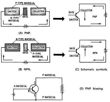
Fig. 8-1. Transistors.
Part C of Fig. 8-1 shows the schematic symbols for the two types. The only difference between the symbols is the direction of the arrow. As in all semiconductor schematic symbols, the arrow points in the direction opposite to the flow of electrons. It is important to note that in the external part of a circuit which uses a PNP transistor, electrons flow toward the collector. This means that a PNP transistor will have its collector connected to the negative side of the battery.
In a PNP transistor, both the emitter and collector are P-type material, but each has a different biasing arrangement. The emitter-base junction is said to be forward-biased, while the collector is reverse-biased with respect to the emitter.
As shown in part D of Fig. 8-1, the positive side of the emitter base battery is connected to the P-type material, which is the emitter. The negative terminal of the collector battery is connected to the collector, which is P-type material. Thus, it can be seen why the emitter is said to be forward biased and the collector reverse biased.
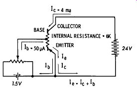
Fig. 8-2. Current in transistor.
In Fig. 8-2, a greatly simplified schematic diagram shows the effect of the base section of a PNP transistor. The base is shown containing an adjustable resistor. The resistance of this base region varies with the amount of current flowing through the base, and this small current has a large effect on the current flow between the emitter and collector.
The base current, lb, is normally from 10 microamps to about 300 microamps and must be supplied from some regulated DC source. This current is the "fuel" which keeps the current in the transistor flowing from the collector, through the base, and out the emitter. If the base current stops, then the main current, le, will also stop. A slight change in h results in a relatively large change in le. This action makes it possible for the transistor to amplify.
Fig. 8-2 shows the following current directions in the circuit:
Base current, I_b: From the 1.5V battery, through the base, out the emitter, and back to the battery.
Collector current, I_e: From the 24V battery, through the collector, through the resistance of the base, out the emitter, and back to the 24V battery.
Emitter current, I.: The sum of 10 and lb flowing out of the emitter, dividing into separate currents, and returning to their respective batteries.
A basic relationship of currents in transistor circuits is, therefore:
I_e= I_e+ I_b
In small transistors the base current is small, so the emitter current is often taken to be equal to the collector current, with the base current being ignored completely.
To see how a transistor amplifies, assume that 50 microamps of lb is flowing in the circuit in Fig. 8-2, and that this brings the adjustable base resistance to 6000 ohms. When, It> = 50 microamps: E 24V
l_e = R = GK = 4 ma
If the base current increases to 75 microamps, and if this causes the internal resistance of the transistor to decrease to 4K, then the new collector current is: 24V le= 4K = 6 ma
If the base current decreases to 25 microamps, and if this causes the internal resistance to increase to 12K, then the new collector current is : 24V
l_e= 12K = 2 ma
Note that a change of ± 25 microamps in base current results in a change of ± 2 milliamps in collector current.
In the preceding circuit, no output signal can be taken between the collector and emitter because this voltage is always equal to the battery voltage. To see how output voltage is taken, consider the circuit in Fig. 8-3. This circuit has a collector resistor, R_c, and uses a 2N414, which is a typical small signal PNP transistor. The characteristics are shown on the graph in Fig. 8-4.
At Point 1 on the Graph: I_b = 50 microamps
The collector current depends on the internal resistance of the transistor, and is obtained from the graph: le= 2.5 ma
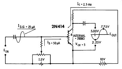
Fig. 8-3. Voltage across transistor elements.
The voltage from collector to emitter, as indicated by the graph, is:
Vce= 5V R Vee 5V 2000 h Internal = L = 2.5 ma = 0 ms
If a signal is now applied which increases lb to 75 microamps, then: At Point 2 on the Graph: lb = 75 microamps le= 3.75 ma Vee= 2.25 volts
Fig. 8-4. Characteristic curve of a typical PNP transistor.
R_internal is now : 2.25V 3_ 75 ma= 600 ohms
When the input signal reduces lb to 25 microamps, then: At Point 3 on the Graph: lb = 25 microamps Vee= 7.75 volts le= 1.25 ma R_internal = 6.2K
Thus, it can be seen that when an incoming signal causes the base current to vary, the internal resistance of the transistor will change, causing large corresponding changes in the collector current. Also, voltage V0 ~, from collector to emitter, will vary according to the input signal, and this is an amplified version of the input voltage.
If the output is taken from across the collector and emitter terminals through a capacitor, the stage becomes a voltage amplifier. If variations in le are passed through an inductance, the stage can be a power amplifier.
In the above example, we found that a change of± 25 micro amps in lb would cause a change in the internal resistance of the 2N414 transistor, resulting in a change in le of ± 1.25 ma.
The relationship between the change in base current and the resulting change in collector current is a very important characteristic of each individual transistor. It is given in the manufacturer's specifications as /3 (beta) and is called the gain of the transistor. Some manufacturers designate this as Hre• It is the ratio of:
/3 _ change in le
- change in lb
The value of /3 will range from 10 to 200, with 50 being about average. In our example, the transistor we used had a f3 of:
or le_ 1.25 ma lb - 25 microamps 1.25 X 10^-3 = .05 X 103 25 X 10^-6
/3 = 50
It should be noted that the presence of R,. = 2K in the circuit of Fig. 8-3B makes it possible for the output voltage, Vce, to vary. The peak-to-peak swing of V, .• is dependent on the value of Re as indicated by the slanted line on the graph. This line is called the load line. In our example, the peak-to-peak swing of Yee is from 7.75 to 2.25, or 5.5 volts. To become more familiar with the effect of Re, the reader should repeat the preceding calculations, finding all the new values when Re = 2.5K. The new load line will cross the horizontal axis at Yee = 10, and the vertical axis at I,. = 4 ma. The peak-to-peak swing of V_ce will then be approximately 6.5 volts.
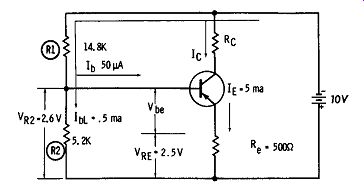
Fig. 8-5. Method of obtaining base bias.
BIASING AND STABILITY
The circuits we have been discussing are not practical for two reasons :
1. A separate battery source was used for base current.
2. There was not sufficient control over unwanted variations in the base and collector currents due to leakage and heat.
A popular method for using a single battery is illustrated in Fig. 8-5. R1 and R2 form a voltage divider across the collector battery so that the 10 volts will be divided across the two resistors. The base-to-emitter voltage, which is the for ward-bias voltage, is the difference between V,2 and Yr.: Yre - V,2 = Vbe 2.5 - 2.6 = 0.1 volt
The bleeder current flowing in R2 and neglecting I_b = 50 uA is approximately: 0.5 ma
In addition to the bleeder current, the base current of 50 microamps flows in R1. It can be seen that the base current is a very small part of the total current in R1, and therefore has negligible effect on voltages V rt, V r~, and V re•
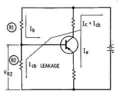
Fig. 8-6. Direction of I_cb. leakage.
The stability of the bias bleeder system is very important since any slight change in the base current will result in a large change in collector current, especially when the beta figure is high : I,.= /3l0
In order to keep the collector current within the maximum limits of the transistor, and also to insure that the output signal will not be distorted, it is essential that the base bias voltage does not drift.
The two main causes for changes in the base bias voltage or current are: (1) heat generated in the transistor causing leakage, and decreasing the resistance from base to emitter, and (2) changes in the battery supply voltage. The former is by far the most important.
The leakage current, 1,.1., shown in Fig. 8-6, is present in all transistors and is the cause of the principal disadvantage of all semiconductors as compared to vacuum tubes. This leakage current is sometimes specified by manufacturers under only one set of conditions. However, it increases in proportion to the temperature of the junctions in the transistor. l,.11 exhibits the following characteristics:
1. It doubles for each 10°C of junction temperature in germanium transistors.
2. Its direction is always in opposition to the desired base current.
3. It causes an increase in collector current which is uncontrolled by the base current.
Thus, the base voltage, Vr2 in Fig. 8-6, must always be well regulated. The regulation is usually achieved by use of a voltage divider such as R1 and R2.
Voltage measurements in the biasing system are so important to successful troubleshooting in transistor circuits that we will take one more example:
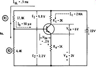
Fig. 8-7. Bias-voltage measurements.
In Fig. 8-7, a transistor is shown in which there is 2 ma of le when Vbe = 0.2V, lb= 50 microamps and Vee= 6V. Neglecting lb as part of le, then*: R
_ 10 Vbe _ 2V _ l000 h
.- ---- oms
· I. 2 ma V. = 1000 x 2 ma = 2V To find the value of E2: E2 must be larger than V. by the amount of the required Vb.: E2 = V. + Vbe
= (2) + (.2)
=2.2V To find the value of El: El= 12- E2
= 12 - 2.2
=9.8V
* R. is usually chosen to make V .. = 10 Vb•
This ensures good stability.
To find the value of R2:
First choose any small bleeder current, l1>1
It is standard de sign practice to choose lb1 ten times the required base current it is supposed to stabilize.
Then: lb!= 10 lb
= 10 x 50 microamps
= 500 microamps (or 0.5 ma)
R2
= E2 = 2.2V = 4.4K l1,1 0.5 ma
To find the value of Rt:
The current through R1 is the sum of: and:
lrl = h1 + lb
= 0.5 ma+ 50 microamps
= 0.5 ma + .05 ma
= 0.55 ma R1 = El lr1 9.8V
0.55 ma
= 17.8K
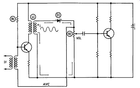
Fig. 8-8. Simplified AVC circuit.
Almost every failure in transistor circuits will cause a change in one of these values. The necessity for understanding these calculations arises from two facts: ( 1) all the values are interdependent, and a change in one causes changes in others; and (2) all this information about the circuit is not given in the schematics, so the technician may have to calculate to find whether some measured value is correct in relation to other measurements.
AUTOMATIC GAIN CONTROL OF TRANSISTOR STAGES
The partial schematic in Fig. 8-8 illustrates the A VC connections in transistor receivers. The bleeder system which sets the base voltage is modified somewhat. Resistor R1 is still present and still returns to the negative battery line, but the second resistor, R2 in the bleeder system, is missing. It is replaced by the volume control, which also serves as the detector load resistor.
Notice the loop consisting of L1, D1, and the volume control.
The bottom end of L1 is returned to the positive battery line.
The cathode of the diode returns, via the volume control, to the same point.
With no bias on the diode, a signal voltage, el, appears in L1 and causes current to flow in the direction shown on the half-cycle when the diode plate is positive. In this way, the carrier is rectified, and audio variations appear across the volume control. This is like the familiar tube-type detector circuit.
The difference to be noted in PNP transistor circuits is that the polarity at the top of the volume control is positive. It is at this point that the AVC line is connected. So, the AVC voltage applied to PNP stages is a positive voltage with respect to the emitter which is returned to the bottom of the volume control.
The resistance of the volume control takes the place of R2 in the base voltage-divider system. This resistance provides fixed bias when there is no signal and makes the base of the IF stage more positive (less negative) when a carrier appears at the detector diode.
The troubleshooting technician must realize that when PNP's are used in the IF stages, the base must always be negative with respect to the emitter. While the AVC voltage is positive, it is very small and causes only a slight change in lb. If the base voltage on a PNP in an IF stage is ever found equal to the emitter, or positive with respect to it, the stage is not operating correctly.
Fig. 8-9 shows two circuits in which the A VC line is connected to the "cold" end of the 1st IF-transformer secondary.
A VC is not always applied to all stages because of the different base currents required by various transistors. Also, a separate resistor is sometimes used for the detector load, rather than using the volume control. The examples shown in Fig. 8-9 are typical.
C15 in Fig. 8-9A is the IF bypass capacitor across the detector load. Its purpose is to present a low impedance to the IF carrier and sidebands so that they will not develop voltage across the detector load resistor. The beat frequency between the sidebands and the carrier is the desired audio signal which produces voltages across the load resistor, since audio frequencies are not shorted out by the bypass capacitor. This capacitor plays no part in the A VC, but leakage here will reduce the AVC voltage. If C15 in Fig. 8-9(B) is shorted or leaky, it will reduce the audio signal and destroy the fixed bias on the IF stage, because R15 is part of the base-bias voltage divider. This condition may be confusing to the trouble shooter because the receiver appears to have two different troubles-the audio system is not working, and one IF stage may be cut off.
(A) Ungrounded detector load resistor. (B) Grounded detector load resistor.
Fig. 8-9. Typical AVC circuits.
R14 and C14 in Fig. 8-9(B) form the AVC filter. They serve the same purpose as similar components in a tube-type receiver. However, the value of the resistor is much smaller and the value of the capacitor much larger in transistor receivers. A shorted capacitor affects the bias of the IF stage as described before. An open capacitor allows the base voltage to vary with the audio modulation, producing distortion. The distortion is much greater in transistor circuits than in tube type receivers when the AVC filter capacitor is open, however.
C11 and C12 in Fig. 8-9A are neutralizing capacitors to provide negative feedback, preventing the stage from oscillating. The internal capacity of a transistor is greater than that of a vacuum tube, and positive feedback from the collector to the base occurs. The capacitors are chosen to be equal to the internal capacity, and will provide sufficient negative voltage feed back to cancel the effect of the internal capacity.
Diode D1 is called an auxiliary A VC, and is for overload protection in the event of a large signal input. The operation is explained in Fig. 8-10. Part A shows the circuit of Fig. 8-9B, but redrawn without resistors R1 and R2.
The resistance of the diode essentially shunts the primary of L1 so that when the internal resistance of the diode is low, the output of the first stage is reduced. Part B of Fig. 8-10 shows the connections redrawn without the coils to show the DC circuitry involved.
(A) Fig. 8-7B redrawn without resistor. (B) DC circuitry of D1.
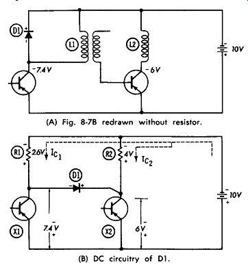
Fig. 8-10. Auxiliary AVC simplified.
The voltages on the diode cathode and anode are determined by R1, R2, and the collector-emitter resistances of the transistors. The cathode voltage measured to ground is -6V, and the voltage on the anode is -7.4V. The diode is reverse-biased, and its resistance is extremely high, making negligible its effect in the circuit of part A. However, if a strong signal were applied, the collector of Xl might drop to -5 volts due to increased collector current through R1. The diode would then conduct because its anode would be positive with respect to the -6 volts on its cathode.
In this condition, the internal resistance of the diode is lowered, and its shunting effect is greater.
In addition, the overload protection is enhanced by the normal action of the receiver's A VC. An increase in signal strength is reflected as a decrease in the negative bias on X2, and its collector current is reduced. This makes the cathode of the diode more negative because of less drop through R2, with resulting lower resistance shunting the primary of T1.
The reverse bias on the diode under normal signal conditions is set by the circuit designer so that the diode does not begin to conduct until after a predetermined signal strength has been reached. With judicious choice of diode characteristics and bias voltage, this circuit is a very effective auxiliary AVC. Symptoms of failure important to the troubleshooter will immediately suggest themselves. High leakage or low internal resistance in the diode produces excessive shunting action across the output coil. A change in R1 or R2, or in the characteristics of the transistors, upsets the intended reverse bias on the diode.
POWER SUPPLY AND DECOUPLING
Transistor circuits are much more sensitive to change in the power-supply voltage than vacuum-tube circuits. Also, since the supply voltage is small for the amount of power delivered, the current drawn is much greater than in a comparable vacuum-tube circuit using voltages in the vicinity of 100 volts. This means that the transistor power supply must have low internal resistance, and somewhat better voltage regulation than is found in power supplies for home-type vacuum tube radios.
A battery is therefore the natural choice of power source for transistorized equipment, and several types have been especially developed for this application. The construction and specific characteristics of the batteries are not of much concern to the technician, except to note that the internal resistance must be low to give the required voltage regulation with the varying current load. The internal resistance of batteries tends to increase as they become exhausted with use, or even as they age on the shelf, and this leads to many symptoms of failure in transistorized equipment. A check of the battery terminal voltage under load is therefore one of the early tests that should always be applied to transistor radios which do not perform properly.
Many technicians have devised home-made AC power sup plies to use on transistor receivers undergoing tests and repair. The ordinary battery eliminator used for auto radios usually works well if its voltage output is adjustable. These eliminators have the necessary low internal resistance. In some cases, it is helpful to add a 500- to 1000-mfd electrolytic capacitor across the output terminals to improve the filtering.
Many technicians are surprised to find a complete pi-type RC filter included in battery-powered transistor radios. Fig. 8-11 shows a few examples taken from actual circuits. The capacitances used are likely to be somewhat higher than those in vacuum-tube radios because the current variations will be greater. The value of the series resistor is smaller for the same reason. The voltage ratings of the capacitors will be less than 25V. Failure of these units is just as common as it is in tube type receivers, but the symptoms are different.
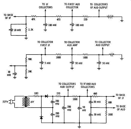
Fig. 8-11. Examples of decoupling.
When batteries are used, there is no 60- or 120-cycle hum to be filtered. The purpose of these capacitors is to maintain the supply voltage constant with the large current variations resulting from the demands of the transistor audio output stage which must furnish the necessary audio power. The filter is actually an audio bypass across the battery. This kind of filtering is called decoupling.
In addition to the decoupling at the battery, transistor radios usually have several other decoupling filters inserted in the supply lines to the various stages. (See Fig. 8-11.) The general rule for the value of the resistor and capacitor in decoupling networks is that the resistor should be 1/10 of the impedance in the collector or emitter circuits of the stage, R.nd the reactance of the capacitor should be 1/10 of the resistor value at the lowest frequency to be filtered.
AUDIO OUTPUT STAGES
The power output stage in pocket-type transistor radios delivers from 0.1 to 0.5 watt of power. The larger receivers can produce from 1 to 3 watts. While these seem to be very small amounts of power, it is important to remember that the voltage supplied to the output stage is seldom more than 9 volts. If 2 watts were to be developed, this would require approximately 220 ma of current from the battery. The problem of maintaining a stable output voltage from the battery supply becomes more difficult as the power-output requirement increases, and symptoms resulting from defective decoupling circuits are more prevalent.
In order to obtain better efficiency in the output stage, and to allow the use of smaller transistors, the stage is almost always a push-pull circuit operating close to class B. This means that the transistors will have very little forward bias, which means that they are nearly cut off when no signal is applied.
It is interesting to note that if one transistor in a push-pull output stage is disconnected, the change in the output from the speaker is barely noticeable. But the technician must realize that the one remaining transistor is now subjected to much different operating conditions. Some typical push-pull stages are shown in Fig. 8-12.
Notice that transformer coupling is most commonly used throughout. This method is somewhat more expensive, and the fidelity is limited by the transformer. When one considers these disadvantages in addition to the fact that transformers are large and relatively heavy components to be included in miniature radios, the transformer-coupled circuit seems a poor choice.
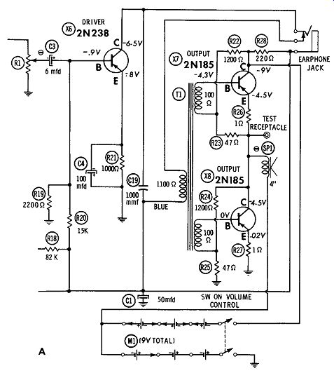
Fig. 8-12. Transistor push-pull output stages.
However, the loss of fidelity is not an important factor in the smaller radios, since the speaker and cabinet enclosure must be so small that the fidelity is limited anyway. The cost of the transformer is offset by the increased efficiency obtained, and by the possibility of matching any inexpensive speaker.
The output transformer is eliminated in the circuit shown in part A of Fig. 8-12 by placing a special speaker in series with the emitter-collector line. The transistors are driven 180° out of phase and are in series for the output current. When the upper transistor is conducting, the lower one is going out of conduction, and thus current from the emitter of the upper transistor returns through the speaker. When the lower transistor conducts and the upper one is out of conduction, current is drawn up through the speaker.
Audio Distortion
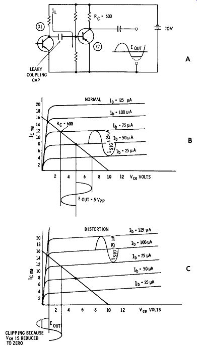
Fig. 8-13. Audio distortion.
An example of one way in which distortion can occur due to a component failure is shown in part A of Fig. 8-13, in which two audio voltage amplifiers are resistance coupled. If the coupling capacitor between the two stages is leaky, an unwanted current, Ir,, will flow through the capacitor, increasing the forward bias on the base of X2.
Suppose that X2 were originally biased at 50 microamps of base current, and that the incoming signal consists of ± 25 microamps. Without the leakage, the base current of X2 was supposed to vary from 50 to 75 microamps on one half of the input cycle, and from 50 to 25 microamps on the other half.
As shown on the graph in part B of the illustration, this would cause a change in the output signal voltage, V,.., corresponding exactly to the shape of the input waveform. This shows a correctly operating class-A stage with no distortion.
The results of the leakage, Ir,, through the coupling capacitor can be seen in part C. Assume that the capacitor leaks enough to increase the forward bias to 100 microamps. The same signal input now starts its swing from the line, l1, = 100. The upward swing of the base current to 125 microamps should cause about 19.5 ma of collector current to flow, except that the load line shows this to be impossible.
19.5 ma of current through the 600 ohms of Re would result in 600 x 19.5 ma = 11.7 volts dropped across R0. But the battery voltage is only 10 volts, so only 10 volts can appear across Re. This will reduce Yee to zero. The output signal, Yee, drops to zero before the input signal has reached its peak, and the result is clipping on half of the output waveform.
Similar results can occur from a change in the value of Re which changes the slope of the load line, or from excessive input signal. The same kind of distortion is cause by over heating in high-power transistors.
An emitter resistor greatly improves the biasing stability.
If one had been used in our example here, much more leakage could be tolerated before clipping would occur, because the increased collector current would make the emitter more negative, reducing the forward bias.
Transistorized Hi-Fi
Transformerless high-fidelity transistorized output stages are used in larger, more expensive equipment. One circuit is shown in Fig. 8-14. * This amplifier illustrates some features of interest to the troubleshooter.
Fuses are used in the emitter leads of X4 and X5. Besides providing protection against transistor burnout due to excessive current, the fuses also give additional stabilization because they insert about 1 ohm of emitter resistance. X2 and X3 are biased by the 1N91 diodes. (The voltage drop across a diode, after it begins to conduct, is practically constant over a large range of current.) This method of stabilization is frequently used in more expensive equipment. A large amount of negative feedback is used, as is common practice in transistorized high fidelity equipment. The amplifier is described as capable of delivering, with a 1-volt input, 8 watts output directly into an 8- or 16-ohm speaker. Practically flat response from 30 cycles to 50 khz with a 1-watt output is possible.
* This circuit is described fully in the General Electric Transistor Manual, 1962, p. 130.
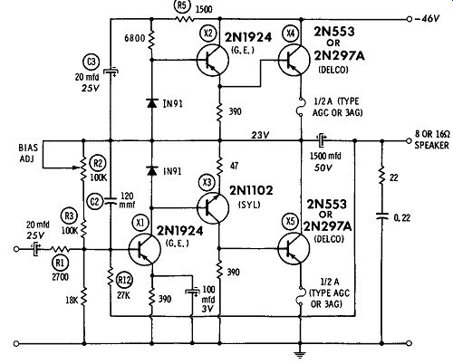
Fig. 8-14. A high-fidelity transistor amplifier.
Troubleshooting this type of equipment is not difficult be cause the critical components can be seen immediately in the schematic. Failure of the 1N91 diodes, for example, upsets the biasing of X2 and X3 with consequent distortion or changes in gain. Leakage or a change in value of the electrolytic capacitors or resistors in the feedback circuits, such as R5 and C3, results in loss of gain or distortion. Replacing one of the fuses with a type having a different resistance will change the bias on one of the transistors. X4 and X5, as well as X2 and X3, are operating in class-B, and so the technician should look for changes in the forward bias when there is loss of gain. The forward bias on a class-B stage should be almost zero to keep the transistors practically cut off when no signal is applied.
When one transistor fails in a push-pull combination, such as the ones used in this circuit, the change in output from the speaker is definitely noticeable.
THE MIXER/OSCILLATOR STAGE
The circuitry of the converter stage is not as well standardized in transistor receivers as it is in vacuum-tube receivers, and nearly every model will have some variations. In addition, many of the better transistor receivers include an RF amplifier stage between the loop antenna and the converter.
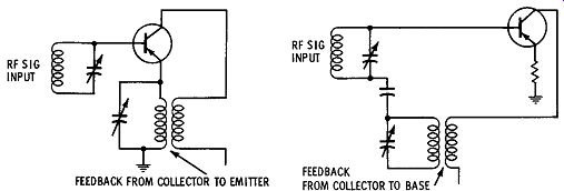
Fig. 8-15. A simplified mixer/oscillator stage.
Two elements of the converter circuitry which most stages have in common are shown in Fig. 8-15. The RF input signal is fed to the base, and there is always a provision for feedback either from the collector to the emitter, as shown in Part A, or from the collector to the base, as shown in Part B. The operation is essentially the same in both circuits. The current from the collector excites the tuned circuit in the feed back transformer, thus setting up oscillation. The feedback transformer is tuned 455 khz higher than the incoming RF signal to provide the proper beat-frequency.
Whether the oscillator signal is fed into the emitter or coupled to the base through a capacitor makes very little difference. In both cases, it will mix with the incoming RF, and the beat at 455 khz can be taken from a tuned transformer inserted in series with the collector. For simplicity, this output trans former is omitted in Fig. 8-15, as is the biasing network.
Fig. 8-16 shows a complete stage, including:
1. C1 and C2, the main tuning capacitors coupled to the same shaft.
2. C3 and C4, the screwdriver-adjusted alignment capacitors for adjusting the tracking.
3. T1, the oscillator tuned circuit operating at 1175 khz when the radio is tuned to a station at 720 khz.
4. R1 and R2, the biasing network which fixes the base voltage.
5. T2, the output transformer tuned to 455 khz, the difference beat between the incoming RF and the oscillator signals.
6. C5, which couples the oscillator signals.
7. C6, which prevents the bias voltage from being shorted to ground through the loop antenna.
8. R3 and C8, a decoupling network which prevents the collector signal from appearing in the base bias network and thereby being fed back to the base.
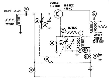
Fig. 8-16. A complete mixer/oscillator stage.
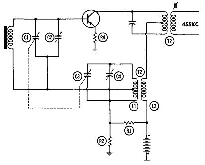
Fig. 8-17. A mixer/oscillator stage with tapped coils.
Fig. 8-17 uses feedback from collector to base, and employs tapped coils. The variations are endless, and each must be studied for differences which determine the approach the troubleshooter will take. Besides knowing the key test points to be described in Section 9, the technician must realize that the circuit performs two functions-the amplification of in-coming signals, and the generation of the oscillator signal.
When certain of the components are defective, both functions will be disabled; in other cases only one of the functions fails.
Symptoms and testing techniques are classified accordingly.
In Fig. 8-16, if either L1 in the oscillator transformer, or C5 fails, only the oscillator will be disabled, and the radio will still respond normally to a 455- khz signal fed to the base from a signal generator. But if the lower part of L1 in Fig. 8-17 were open, the entire stage would be dead because of loss of forward bias on the base.
Similarly, the technician would take a different approach to the two circuits if the antenna coil were open. In Fig. 8-16, the oscillator would still be operating but no stations could be tuned in. Fig. 8-17, the oscillator would not be running.
In Fig. 8-16, a shorted RF tuning capacitor, C1, will stop the oscillator by removing the base bias; in Fig. 8-17, it would not.
QUIZ
1. Look up the characteristics of three PNP transistors.
a. One suitable for the converter stage in a broadcast receiver.
b. One suitable to drive a high-powered audio-output stage.
c. One suitable for use in a 10-watt, push-pull, audio output stage.
State:
1. Maximum collector-to-emitter voltage for each.
2. Maximum collector current for each.
3. Operating temperature for each.
4. Leakage current for each at a specific temperature.
Make a sketch of each, labeling the three terminals.
2. Look up the schematic of a radio which uses separate transistors for the oscillator and converter, and draw the circuits.
3. Construct a graph showing the load line and operating point of the transistor stage shown.
4. In the circuit on page 130, the input signal swings ± 50 microamps. What is the peak-to-peak output voltage?
5. Using a transistor which has 4 ma of collector current when V_ce is 6 volts, an I_b of 20 microamps, a V be of 0.2 volt, and using a 9V battery, draw the schematic of a voltage amplifier suitable to follow the detector in a receiver. Include a volume control, a tone control, emitter resistor, and biasing network. Label the values of all parts.
6. In what way is the A VC in a transistor radio different from that in a vacuum-tube circuit? Illustrate with partial schematics.
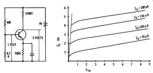
7. In the circuit below, a technician measured the two voltages indicated. By making some calculations and referring to the collector-characteristic graph, he was able to deter mine whether the stage was operating correctly. Perform the necessary calculations and state whether the stage is operating normally.
8. Look up the schematic of a converter circuit, and make a drawing of a stage.
a. Indicate one component whose failure would prevent reception of station but leave the oscillator running.
b. Indicate one component whose failure would stop oscillation without preventing passage through the stage of a 455- khz signal injected at the antenna.