CONTRAST CONTROL: The contrast control of a television receiver is similar in function to the volume control of the broadcast or communication receiver. By contrast is meant the ratio of the light intensity of the brightest highlight in the picture to that of the deepest shadow. Due to scattering of light at the fluorescent surface, the black of the shadow can never be an absolute black, or absence of light. Since this ratio, of maximum illumination to illumination at the cut-off point, is directly proportional to the voltage swing of the control grid of the picture tube, it is evident that the contrast can be controlled by varying the output of the video amplifier. Output control can be achieved also in the RF amplifier, the first detector or the IF amplifier. A combination of control at several points in the system is frequently employed.
CONTRAST CONTROL BY CHANGE OF VIDEO AMPLIFIER GAIN. Figure 238A and B shows two methods of controlling the output of the video amplifier. At A the contrast control is identical to the familiar audio volume control which is a potentiometer functioning as the second detector load. Circuit elements C1 and L1 are employed for video high frequency compensation.
At B, of Figure 238, a variable cathode bias resistor of one of the video stages is employed to change the operating point of the tube and hence its transconductance or gain.
In this case, the control is left unbypassed so that the degeneration introduced by the resistor is the same at all frequencies and does not affect the bandwidth of the amplifier.
A. CONTRAST CONTROL BY POTENTIOMETER; B. CONTRAST CONTROL BY VIDEO AMP BIAS; C. CONTRAST CONTROL BY CHANGE Of VIDEO If BIAS
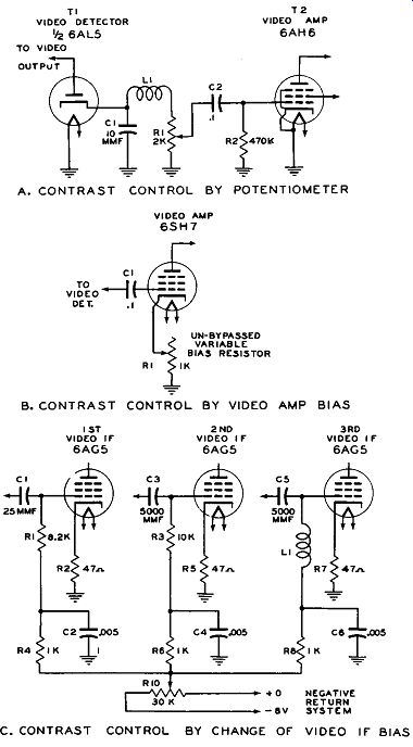
Fig. 238. Contrast Control by
Change of Video Gain.
CONTRAST CONTROL BY CHANGE OF VIDEO IF AMPLIFIER BIAS. Figure 238C shows a method of contrast control in which the gain of three stages of the video amplifier is adjusted by change of grid bias. This grid bias is developed below ground potential. Several methods of deriving a negative voltage for this control purpose are employed:
1. The power supply system has an intermediate point in a voltage divider connected to ground rather than the center tap of the supply transformer tube. 2. A selenium rectifier is used to derive approximately 8 volts DC from the 6.3 volt AC filament supply. (The peak of the 6.3 volt AC wave is 8.9 volts.) 3. The negative bias developed in the grid of the horizontal scanning oscillator is filtered and used as a source of contrast control voltage.
CONTRAST CONTROL BY DIVIDED BIAS ON RF AND IF STAGES. An important consideration in the design of gain control by variation of bias in the RF and IF amplifiers is to avoid grid overload of any of the stages under control, by the signal. Since sharp cut off tubes such as the 6AG5 and 6AU6 are frequently employed in the video IF amplifier in combination with tubes of a more extended cut off, such as the 616 in the RF amplifier, a bias system which supplies more control voltage to the 616 is required.
Figure 239 shows a system in which the bias on the 616 RF tube varies from -1.1 volts to -8 volts, while the bias on the 6AG5 video IF tubes is controlled from -1.1 to 15 volts.
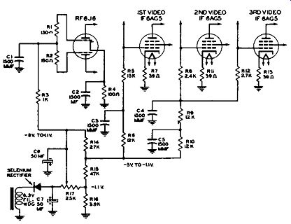
Fig. 239. Contrast Control by Divided Bias.
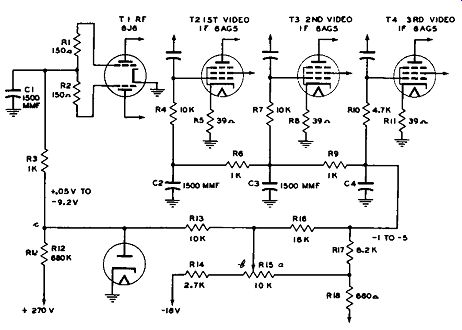
Fig. 240. Use of a Diode Gate to Provide Improved Contrast Control Action.
Full Control on RF Stage--Partial Control on IF Stages.
THE DIODE "GATE" AND ITS FUNCTION IN A CONTRAST CONTROL SYSTEM . Figure 240 shows a refinement of the divided bias system of Figure 239. In this case a novel arrangement of employing a diode is used in conjunction with the control circuit. The primary function of the diode is to allow the RF stage to run at full gain over a considerable range of the contrast control. This assists in maintaining a high signal-to-noise ratio. The gain of the RF stage is reduced only when it becomes necessary in order to prevent over load of the first IF stage. The operation of the circuit is as follows:
When the contrast cont r ol(R15) is at maximum gain position, "a", the bias on the video IF amplifier is approximately -1 volt.
The RF bias, taken from the tap "c" on the divider network connected to +B would be several volts positive if it were not for the heavy conduction of the diode. (The diode resistance when conducting is only a few hundred ohms.) This holds the RF bias at approximately zero. As the contrast control is moved away from its maximum position the RF and IF biases fall as shown in Figure 241. The IF bias immediately goes negative to produce the major portion of the gain control. Diode conduction decreases and at approximately 75% of maximum rotation the slope of the RF bias changes more rapidly. As the contrast control is reduced still further, the diode conduction stops and the RF bias voltage proceeds at an even more rapid rate and passes that of the IF bias. Although triodes are normally not considered to be remote cut-off tubes, sufficient .... .... curvature of the grid bias versus transconductance curve exists in the case of the 616 to permit approximately 10/1 gain reduction over the range shown in Figure 241. This prevents overload at any point in the control range.
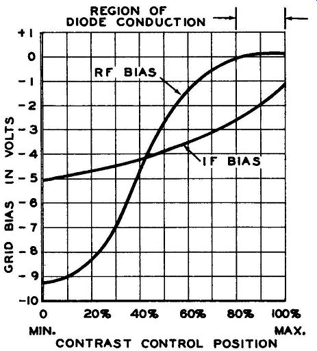
Fig. 241. Bias Characteristics of the Circuit Shown in Figure 240.
Fig. 242. Station Test Pattern Showing the Effect of Misadjustment of the
Contrast Control. Photo.
A.G.C. (AUTOMATIC GAIN CONTROL): The television service technician is familiar with automatic volume control in standard broad cast and short wave receivers. Its purpose is to compensate automatically for fading , and also to hold the gain of the receiver constant as it is successively tuned to stations of varying carrier strength. Actually the A. V. C. system of a broadcast receiver is an A.G.C. system, because the function of volume control is normally accomplished by variation of the audio gain. In a television receiver, the A. G. C. system functions to hold the overall gain or contrast constant, as the receiver is tuned to various channels representing stations of various carrier strengths. It is not normally called upon to compensate for fading because, in the majority of cases, the receiver is being operated in a region of fairly constant field strength, (the primary service area). In fringe reception, however, the additional function of compensation for fading is present.
Another function of A.G.C. is to hold the video voltage constant and thus line up the tips of the sync pulses. This is of importance in receivers of the triggered sync type which do not have the advantage of automatic frequency control sync system.
Figure 243 shows a circuit in which an A.G.C. diode (T4) is connected in parallel with the video detector by means of the coup ling capacitor (C5). The diode rectifies the video IF envelope and the capacitor C5 is charged to a value determined by the tips of the sync pulses. The combination of resistor R8 and capacitor C5 represents a long time constant (approximately 0.2 second). This tends to average short time variations of the carrier.
Coupling network R7-C4, filters the detector output and provides a DC control voltage for the grids of the RF and IF-amplifier. In the example shown, sync separation is accomplished by dividing the diode load and taking the sync pulses from the cathode.
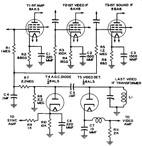
Fig. 243. Basic Automatic Gain Control Circuit.
A significant difference between the operation of the A.V.C. of a sound receiver, and the A. G. C. of a television set, is the fact that A. V. C. establishes a bias voltage which is proportional to average carrier strength, while A. G. C. assures that the controlling bias is proportional to maximum carrier strength (i. e., the top of the video carrier envelope is held constant , in transmission, at the sync pulse maximum value).
In sound transmission, the carrier envelope constantly changes in accordance with the modulation depth.
AMPLIFIED A.G.C.: A.G.C. systems can employ triode amplification of the rectified carrier voltage in a manner similar to amplified A.V.C. Figure 244 shows such a system.
In this case T1 acts as the A.G.C. diode. The cathode-to-ground circuit is a double section network in which R1 acts as a decoupler and C2 as an RF bypass. The long time constant circuit consisting of R2 (4. 7 meg.) and C3 (.05 mfd.) develops a DC voltage since the capacitor C3 is charged up to the peak value of the sync pulses, and discharges very slowly through R2 during the picture intervals.
Voltage which is fed to the grid of the triode amplifier tube T2 is in the positive direction, but the net operating bias on the grid is maintained in the negative region by the cathode bias. The operating bias is developed in the bleeder circuit from +B, consisting of R4, R5 and the variable resistor R6. R6 is employed to set the point of A.G.C. operation (delay-bias). In addition to the controlling voltage from the A.G.C. rectifier ( T1), a pulsating voltage is supplied to the grid of T2 by injecting some of the output of the horizontal sweep generator through coupling capacitor C4.
The amplified plate current appearing across resistor R7 in the plate of T2 is thus seen to consist of pulses and amplified horizontal sweep voltage controlled in strength by a DC bias proportional to maximum carrier value. This amplified pulsating voltage is impressed on the diodes of T2 through coupling capacitor C5 and is thus rectified to provide the gain control of voltage across the output network consisting of RS and R9. Divided control is again employed to produce a different rate of change of the RF bias.
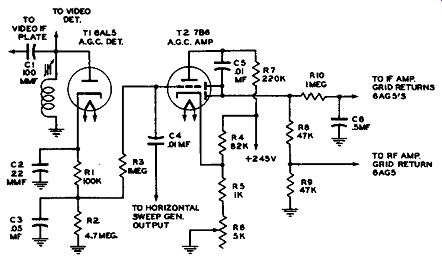
Fig. 244. An Amplified A. G. C. Circuit.
Fig. 245. An A.G.C. Circuit Employing Clipping, Amplification and Gate Action.
NOISE CLIPPING IN A.G.C. CIRCUITS: A refinement of amplified A.G. C., which improves the circuit performance, is the use of diode clippers between the A. G. C. rectifier and the A. G. C. amplifier tubes. Figure 245 shows a circuit which incorporates clipping, amplification, and diode gating (or delay action). The performance of this system is shown in the graph of Figure 246. The use of an elaborate system of this type is justified in deluxe projection models.
In this instance, the time constant of the load circuit of the A.G.C. diode ( T1), has been made much shorter than that of the systems previously described (R2 times C2 = 82 micro-seconds). The diode thus acts as a peak reading voltmeter at the horizontal scanning frequency (15,750 hz).
The fast time constant will allow the system to follow the peak of noise pulses as well as the sync pulse tips. To prevent this from affecting the A. G. C. action, a two stage noise clipping system is employed. It consists of diodes T2 and T3, coupled by resistor R6.
In addition to the clipping action, further protection against noise is provided by feeding the A.G.C. amplifier triode T4, through the integrating circuit consisting of R7 and C3. This circuit removes the effect of random noise.
The delay bias on the clipping diodes T2 and T3, provided by the drop across R3 and the contrast control potentiometer (R4), determines the level at which clipping action occurs.
This same variable bias is applied as an operating bias for the A. G. C. amplifier tube T4, through series resistors R2, R6, and R7, which constitute the grid return of T4. The bias thus establishes the gain of the A. G. C. amplifier, and control R4 can thus act to establish both the gain of the system, and the level at which noise clipping occurs.
Amplifier tube T4 operates with its cathode 110 volts negative with respect to ground, and its plate at, or slightly below, ground potential. Thus, as its grid goes positive with A.G. C. control voltage, the plate goes negative with respect to ground, and the drop across R8 and R9 can act as a control bias for the RF and IF amplifiers. Diode gate tube (T5) performs the same function as described and illustrated in Figure 241.
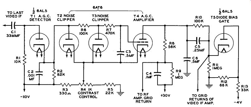
Fig. 245. An A.G.C. Circuit Employing Clipping, Amplification and Gate Action.
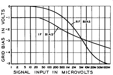
Fig. 246. A.G.C. Bias Versus Signal Input for Circuit of Figure 245.
The overall performance of the system is shown in Figure 246.