1. Power-Supply Terminology
Power Supply. A device that supplies electrical power to another unit. Power supplies obtain their prime power from the ac power line or from special power systems such as motor generators, inverters, and converters.
Rectifier. A device that passes current in only one direction. The rectifier consists of a positive anode and a negative cathode. When a positive voltage is applied to the anode of the rectifier, that voltage minus the voltage across the rectifier will appear on the cathode and current will flow. When a negative voltage is applied to the anode with respect to the cathode, the rectifier is turned off and only the rectifier leakage current will flow.
Forward Resistance. The resistance of an individual cell measured at a specified forward voltage drop or current.
Forward Voltage Drop. The internal voltage drop of a rectifier resulting from the current flow through the cell in the forward direction. The forward voltage drop is usually between 0.4 Vdc and 1.25 Vdc.
Reverse Resistance. The resistance of the rectifier measured at a specified reverse voltage or current.
Reverse resistance is in megohms (M ohm)
Reverse Current. The current flow in the reverse direction, usually in microamperes (µA).
Maximum Peak Current. The highest instantaneous anode current a rectifier can safely carry recurrently in the direction of the normal current flow.
The value of the peak current is determined by the constants of the filter sections. With a choke filter input, the peak current is less than the load current. With a large capacitor filter input, the peak current may be many times the load current. The current is measured with a peak-indicating meter or oscilloscope.
Maximum Peak Inverse Voltage. The maximum instantaneous voltage that the rectifier can withstand in the direction opposite to which it is designed to pass current. Referring to FIG. 1, when anode A of a full wave rectifier is positive, current flows from A to C, but not from B to C because B is negative. At the instant an ode A is positive, the cathodes C of A and B are positive with respect to anode B. The voltage between the positive cathode and the negative anode B is inversely related to the voltage causing the current flow. The peak value of this voltage is limited by the resistance and nature of the path between the anode B and the cathode C.
The maximum value of voltage between these points, at which there is no danger of breakdown, is termed maximum peak inverse voltage.
The relationship between peak inverse voltage, rms value of ac input voltage and dc output voltage depends largely on the individual characteristics of the rectifier circuit. Line surges, or any other transient or waveform distortion, may raise the actual peak voltage to a value higher than that calculated for a sine-wave voltage. The actual inverse voltage (and not the calculated value) should be such as not to exceed the rated maximum peak inverse voltage for a given rectifier. A peak reading meter or oscilloscope is useful in determining the actual peak inverse voltage.
The peak inverse voltage is approximately 1.4 times the rms value of the anode voltage for single- phase, full-wave circuits with a sine-wave input and no capacitance at the input of the filter section. For a single half wave circuit, with a capacitor input to the filter section, the peak inverse voltage may reach 2.8 times the rms value of the anode voltage.
Ripple Voltage. The alternating component (ac) riding on the dc output voltage of a rectifier-type power supply.
The frequency of the ripple voltage will depend on the line frequency and the configuration of the rectifier. The effectiveness of the filter system is a function of the load current and the values of the filter components.
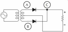
FIG. 1. Peak inverse voltage analysis.
The ripple factor is the measure of quality of a power supply. It is the ratio of the rms value of the ac component of the output voltage to the dc component of the output voltage or
(eqn 1)
where, Vrms is the alternating current voltage at the output terminals, Vdc is the direct current output voltage at the output terminals.
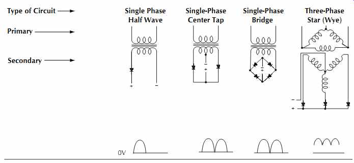
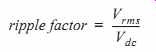
Table 1. Rectifier Circuit Chart
Internal Output Impedance. The impedance presented to the equipment receiving the power supply voltage. In the operation of many devices, it is necessary that the internal power supply impedance be as near to zero as possible. Since most load devices consist of both passive and active elements, the current drawn from the supply consists of an ac component superimposed on the dc output of the supply. The ac component is generally of a nonsinusoidal nature. The output impedance in ohms over a wide range of frequencies is used to determine the regulation of output voltage of a power supply with respect to load variations. Power supply output impedance (Zo) may be defined as

(eqn 2)
where, Eac is the sinusoidal voltage across the power supply terminals, Iac is the sinusoidal current flowing through a series loop consisting of the power supply and load equipment.
Static Line Regulation. The variation in output voltage as the input voltage is varied slowly from rated minimum to rated maximum with the load current held at the nominal value.
Dynamic Load Regulation. The variation in output when the load change is sudden. The power supply may be unable to respond instantaneously, and an additional momentary excursion in the output voltage may result, subsiding afterward to the static load regulation level.
The positive and negative excursion limits are superimposed on the static line and load regulation region. The positive and negative components are not necessarily equal or symmetrical. The most stringent rating is for a change from no load to full load or from full load to no load.
Dynamic Line Regulation. The momentary additional excursion of output voltage as a result of a rapid change in input voltage.
Thermal Regulation. Variations in the output voltage over the rated operating temperature range due to ambient temperature variations influencing various components of the power supply. This is also known as thermal drift.
2. Power Supplies
2.1 Simple dc Power Supplies
The simplest type of dc power supply is a rectifier in series with the load. As more rectifiers are installed into the circuit, along with filters, the power supply becomes more sophisticated. The rectifier in series with the load supply will always remain simple and have poor regulation and transient response. Table 1 shows various power supplies and their characteristics. To determine the value of the parameter in the left column, multiply the factor shown in any of the center columns by the value in the right column.
2.2 One-Half Wave Supplies
A one-half wave unit can be connected directly off the ac mains, FIG. 2A, or off the mains through a trans former, FIG. 2B. Since a rectifier only passes a current when the anode is more positive than the cathode, the output waveform will be one-half of a sine wave, FIG. 2C. The dc voltage output will be 0.45 of the ac voltage input, and the rectifier current will be the full dc current; the peak inverse voltage (piv) across the rectifier will be 1.414 Vac, and the ripple will be 121%. In the transformerless power supply, the 115 Vac power line is connected directly to the rectifier system. This type of power supply is dangerous to both operating personnel and to grounded equipment. Also, power sup plies of this type will cause hum problems that can only be solved by the use of an isolating transformer between the line and power supply.
2.3 Full-Wave Supplies
The full-wave supply is normally used in electronic circuits because it is simple and has a good ripple factor and voltage output. A full-wave supply is always used with a transformer. Full-wave supplies may be either a single-phase center tap design or a full-wave bridge. In either case, both the positive and negative cycles are rectified and mixed to produce the dc output.
The center tap configuration, FIG. 2D, uses two rectifiers and a center-tapped transformer. The Vdc is approximately equal to Vac where Vac is from one side of the transformer to the center tap. Because the output is from each half wave, ripple is only 48% of the output voltage and at twice the input frequency. Each rectifier carries one-half of the load current. The piv/rectifier is 2.828 Vac.
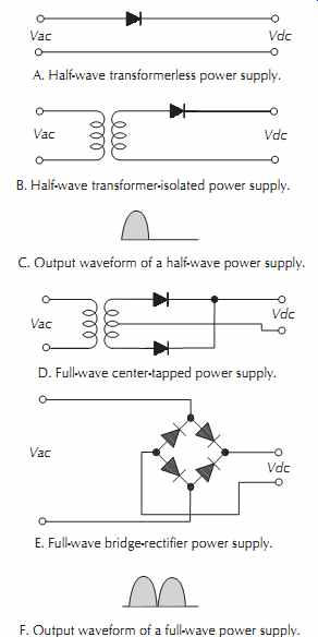
FIG. 2. Two one-half wave and two full-wave power supplies.
A full-wave bridge rectifier supplies full-wave rectification without a center tap on the transformer. The bridge rectifier is not a true single-ended circuit, since it has no terminal common to both the input and output circuits.
A full-wave bridge rectifier consists of four rectifier elements, as shown in FIG. 2E. This circuit is the most familiar and is the type most commonly employed in the electronics industry.
With the full-wave bridge circuit, the dc output voltage is equal to 0.9 of the rms value of the ac input voltage.
Full-wave bridge rectifier circuits may be grounded by three methods shown in FIG. 3A, B, C. Either the input (ac source) or output (dc load) may be grounded, but not both simultaneously. If an isolation transformer is used between the ac source and the input to the rectifier, as shown in FIG. 3C, both ac and dc sides may be grounded permanently. A method of grounding a bridge rectifier is shown in FIG. 3D where the center tap of an isolation transformer is grounded.
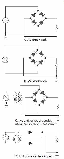
FIG. 3. Methods of grounding a power supply.
When designing rectifier circuits, dc load current, dc load voltage, peak inverse voltage, maximum ambient temperature, cooling requirements, and overload current must be analyzed. For example, assume a full-wave rectifier using silicon rectifiers is to be designed as in FIG. 3D and the dc load voltage Vdc under load is 25 V at 1 A.
Using Table 1, determine the current per rectifier using the equation
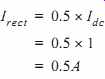
(eqn 3)
where, Irect is the current per rectifier,
0.5 is a constant from Table 1,
Idc is the rectified ac current, which is the dc current.
This is the current each rectifier must carry. Next, the ac voltage required from the transformer is determined by the equation (eqn 4)
where,
Vac is the transformer voltage, 1.11 is a constant from Table 1.
This is the voltage as measured from each side of the transformer center tap; the total voltage across the secondary is 55.50 Vrms.
The peak inverse voltage is
(eqn 5)
where,
Vac is the secondary ac voltage per leg, 2.82 is found in Table 1.
If a rectifier with the required piv rating is not avail able, two or more may be connected in series to obtain the desired piv rating. Unequal values of piv ratings may be used, provided the lowest rating is greater than half of the total piv rating needed.
Parallel operation of rectifiers can be used obtain higher current ratings. However, because of a possible imbalance between the units due to the forward voltage drop and effective series resistance, one unit may carry more current than the other and could conceivably fail.
To prevent this, small equal value resistors must be connected in series with each individual rectifier to balance the load currents, as shown in FIG. 4.
2.4 Three-Phase Power Supplies
Three-phase power supplies are common in the industry but are seldom used to power audio circuits directly.
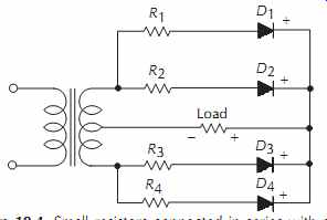
FIG. 4. Small resistors connected in series with each rectifier to balance
the current through each unit of parallel connected rectifiers.
The are used as the input power to power an entire system-for instance, a portable high-power outdoor rock system. To see the characteristics of three-phase sup plies, see Table 1.
3. Filters
A power-supply filter is a series of resistors, capacitors, and/or inductors connected either passively or actively to reduce the ac or ripple component of the dc power supply.
3.1 Capacitor Filters
A capacitor filter employs a capacitor at its input, as shown in FIG. 5A. Power supplies with an input capacitor filter have a higher output voltage than one without a capacitor because the peak value of the rectifier output voltage appears across the input filter. As the rectified ac pulses from the rectifier are applied across capacitor C, the voltage across the capacitor rises nearly as fast as the pulse. As the rectifier output drops, the voltage across the capacitor does not fall to zero but gradually diminishes until another pulse from the rectifier is applied to it. It again charges to the peak voltage.
The capacitor may be considered a storage tank, storing up energy to the load between pulses. In a half-wave circuit, this action occurs 60 times per second, and in a full-wave circuit, it occurs 120 times per second.
For a single-phase circuit with a sine-wave input and without a filter, the peak inverse voltage at the rectifier is 1.414 times the rms value of the voltage applied to the rectifier. With a capacitor input to the filter, the peak inverse voltage may reach 2.8 times the rms value of the applied voltage. This data may be obtained by referring to Table 1.
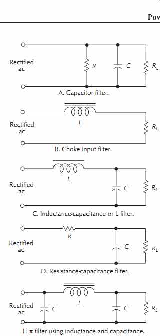
FIG. 5. Capacitive, inductive, and S filters.
When a dc voltmeter is connected across the unfiltered output of a rectifier, it will read the average voltage. As an example, assume a dc voltmeter is connected across a half-wave rectifier. Because of the inertia of the meter pointer movement, the meter can not respond to the rapidly changing pulses of the half-wave rectified current but acts as a mechanical integrator. The pointer will be displaced an amount proportional to the time average of the applied voltage waveform.
The average voltage (Vav), as read by the dc volt meter, is

(eqn 6)
where, Vp is the peak voltage, S is 3.1416….
The ripple factor is (eqn 7)
where, Idc is the output dc current, f is the ripple frequency, C is the filter capacitor in farads, RL is the load resistance in ohms.
Capacitor filters operate best with large filter capacitors and high-resistance loads. As the load resistance is lowered, the ripple increases and regulation decreases.
Filtering efficiency is reduced, and the internal leakage is increased when the capacitor's power factor increases. Electrolytic capacitors should be removed when their power factor reaches an excessive value. In an ideal capacitor, the current would lead the voltage by 90°. Capacitors are never ideal because a small amount of leakage current always exists through the dielectric.
Also, a certain amount of power is dissipated by the dielectric, the leads, and their connections. All this adds up to power loss. This power loss is termed phase difference and is expressed in terms of power factor (PF). The smaller the power factor value, the more effective the capacitor. Since most service capacitor analyzers indicate these losses directly in terms of power factor, capacitors with large power factors may be readily identified. Generally speaking, when an electrolytic capacitor reaches a power factor of 15%, it should be replaced. The filtering efficiency for different values of power factor can be read directly from Table 2.
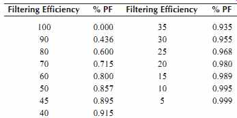
Table 2. Filtering Efficiency versus %Power Factor
3.2 Inductive Filters
An inductive filter employs a choke rather than a capacitor at the input of the filter, as shown in FIG. 5B.
Although the output voltage from this type of filter is lower, the voltage regulation is better.
A choke filter operates best with maximum current flow. It has no effect on a circuit when no current is flowing. The critical inductance is the inductance required to assure that current flows to the load at all times. An inductor filter depends on the property of an inductor to oppose any change of current.
To assure that current flows continuously, the peak current of the ac component of the current must not exceed the direct current Idc
= Idc »RL.
Therefore, 
(eqn 8)
and 
(eqn 9)
where, LC is the critical inductance, RL is the load resistance.
Filter chokes should be selected for the lowest possible dc resistance commensurate with the value of inductance.
The ripple factor (J) for an inductive filter is
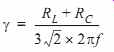
(eqn 10)
where, RL is the load resistance in ohms, RC is the choke resistance in ohms, f is the ripple frequency.
3.3 Combination Filters
Combination filters use a combination of resistors, capacitors, and inductors to improve the filtering. The simplest is a resistor-capacitor filter and the more complicated is a series of inductance-capacitor (LC) circuits.
3.3.1 Inductance-Capacitance Filters (LC)
Inductance-capacitance filters, sometimes called L filters, use an inductor as an input filter and a capacitor as the second stage of the filter, FIG. 5C. LC filters operate well under varying load conditions.
The inductive reactance of the choke in an LC filter section tends to oppose any change in the current flowing through the winding, creating a smoothing action on the pulsating current of the rectifier. The capacitor stores and releases electrical energy, also smoothing out the ripple voltage, resulting in a fairly smooth output current.
The ripple factor for an LC filter is
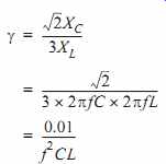
(eqn 11)
where, XC is the capacitance reactance in ohms, XL is the inductive reactance in ohms, f is the frequency of ripple, C is the capacitance in farads, L is the inductance in henrys.
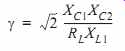
When multiple LC filters are connected together, the ripple factor is
(eqn 12)
where, L is the inductance in henrys, f is the ripple frequency, C is the capacitance in farads, n is the number of sections.
3.3.2 Resistance-Capacitance Filters
Resistance-capacitance filters, RC, FIG. 5D, employ a resistor and capacitor rather than an inductor and capacitor. The advantages of such a filter are its low cost, light weight, and the reduction of magnetic fields.
The disadvantage of such a filter is that the series resistance induces a voltage drop that varies with current and could be detrimental to the circuit operation. An RC filter system is generally used only where the current demands are low. RC filters are not as efficient as the LC type, and they may require two or more sections to provide sufficient filtering.
3.3.3 S Filters
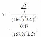
A S (pi) filter has a capacitor input followed by an LC section filter, FIG. 5E. S filters have a smooth output and poor regulation. They are often used where the transformer voltage is not high enough and low ripple is required. By using the input capacitor, the dc voltage is boosted to the peak voltage. The ripple factor for a S filter is
(eqn 13)
where,
XC1 is the capacitive reactance of the first capacitor, XC2 is the capacitive reactance of the second capacitor, RL is the load resistance, XL1 is the inductive reactance of the choke.
When the choke is replaced with a resistor, the ripple factor becomes (eqn 14)
where, R is the filter resistor.
3.4 Resistance Voltage Dividers
A resistance voltage divider is shown in FIG. 6. In this system of voltage division, the resistors are connected in series with the particular load they feed. The resistors are calculated by means of Ohm's law

(eqn 15)
The wattage is computed by

(eqn 16)
Generally, when a series-resistance voltage divider is used, a separate bleeder resistor is also used to secure better regulation. Each section should have a separate bypass capacitor of 10 µF or more to ground. The bypass capacitors stabilize and improve the filtering and decouple the various levels. This is particularly true for the series-type voltage divider.
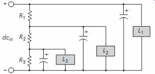
FIG. 6. Shunt-type voltage-divider system showing the current flow in
the various branches.
There are two common types of voltage dividers, the shunt and the series types. The shunt type shown in Fig. 6 is designed to supply three different voltages to external devices. The upper circuit supplies load L1, the second circuit supplies L2, and the third circuit supplies L3. All circuits are common to ground.
The total current required is the total current of the three external circuits, or IL1 + IL2 + IL3, plus an additional current called the bleeder current. This bleeder current flows only through the resistors and not through the external circuits. It is generally 10% of the total current.
Resistor R1 is calculated first, because only bleeder current flows through this resistor,

(eqn 17)
where, V is the L1 voltage also across R1, I is the bleeder current.
The voltage at the top of R2 is the L2 voltage to ground. Subtracting the voltage drop across R1 results in a voltage across R2. The current through R2 is the current of load L1 plus the bleeder current
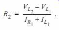
(eqn 18)
Resistor R3 has the current of loads L1 and L2 plus the bleeder current flowing through it or
(eqn 19)
The current of load L3 does not flow through any part of the voltage-divider system; therefore, it requires no further considerations.
4. Regulated Power Supplies
A regulated power supply holds the output constant with variations in load, current, or input voltage. Regulated supplies may be simple shunt or series regulators with 1-3% regulation or high gain supplies with 0.001% regulation and 0.001% ripple.
Power supplies may be connected in parallel, but to protect the supplies, diodes are connected in the positive lead of each power supply. When the diode is in its normal conducting mode, it must be capable of with standing the short-circuit current of its regulator. The piv rating of the diode must be equal to or greater than the maximum open-circuit potential of the highest-rated power supply.
Regulated power supplies can also be connected in series if certain precautions are observed. The isolation voltage rating of the individual power supplies must not be exceeded, and the power supplies must be protected against reverse potential. Diodes are connected in the nonconducting direction across the output of each supply unit. These diodes will start to conduct the instant a reverse potential appears, providing a path for short-circuit current. If possible, the regulating circuit for one supply should be connected as a master and the other as slaves. The voltages of the supplies do not have to be the same.
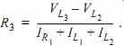
All regulated supplies have a reference element and a control element. The amount of electronics between the two elements determines the quality and regulation of the supply, FIG. 7.
The reference element is the unit that forms the foundation of all voltage regulators. The output of the regulated power supply is equal to or a multiple of the reference. Any variation in the reference voltage will cause the output voltage to vary; therefore, the reference voltage must be maintained as stable as possible.
The control element is that unit that maintains the output voltage constant. The regulator type is named after the control element-namely, series, shunt, or switching, FIG. 7A, B, C. The control element is an electronic variable resistor that drops voltage either in series with the load or across the load. Control element configurations are shown in FIG. 8.
All regulated supplies draw standby current, which is the current drawn by the power supply with no output load. The input voltage to regulated supplies is filtered dc. The smoother the input voltage is, the smoother the output will be. The capacitor C1 shown in FIG. 7A is used to smooth the output or reduce ripple.
The comparison amplifier constantly monitors the output, reducing ripple because the reference voltage is smooth dc and the output ripple voltage appears to the comparator like a varying load. The regulator or pass transistor attempts to follow it, reducing ripple.
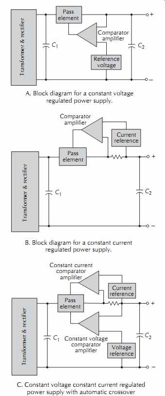
FIG. 7. Regulated power supplies.
A constant-voltage regulated power supply is designed to keep its output voltage constant, regardless of the changes in load current, line voltage, or tempera ture. For a change in the load resistance, the output voltage remains constant to a first approximation, while the output current changes by whatever amount is necessary to accomplish this, FIG. 7A. Its impedance curve is shown in FIG. 9A.
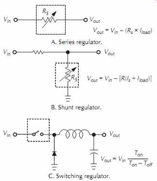
FIG. 8. Examples of various control elements.
FIG. 9. Typical internal impedance characteristics for a regulated power
supply.
An ideal constant-voltage power supply would have zero impedance. For well-designed voltage-regulated power supplies, the internal output impedance will range from 0.001 ohm for frequencies from dc-1 MHz.
The actual impedance is a function of the load and the type of equipment being fed by the supply.
A constant-current regulated power supply is designed to keep its output current constant, regardless of the changes in load impedance, line voltage, or temperature. For a change in the load resistance, the output current remains constant to a first approximation, although the output voltage changes by whatever amount is necessary to accomplish this, FIG. 7B. Its impedance characteristics are given in FIG. 9B.
A constant-current supply would have infinite impedance at all frequencies. However, these ideals are not achieved. Therefore, a practical power supply has a very low impedance at the lower frequencies, and the impedance rises with frequency. The constant-current supply has a rather high impedance at the lower frequencies and decreases at the higher frequencies.
A constant-voltage, constant-current regulated power supply, FIG. 7C, acts as a constant-voltage source for comparatively large values of load resistance and as a constant-current source for comparatively small values of load resistance. An automatic crossover (or transition) between these two modes of operation occurs at a critical or crossover value of load resistance (RC) where

(eqn 20)
where,
Vs is the voltage-control setting, Is is the current-control setting.
4.1 Simple Regulated Supplies
A simple supply consists of only the control element and the reference element. The solid-state zener diode has almost replaced the gaseous tube reference element because it is smaller and has better regulation, wide voltage range, and wide power range. Referring to the basic design in FIG. 10A, the zener diode is connected in series with the limiting resistor R1 and in par allel with the output. As a rule, the zener diode current IZ is chosen for a value of 10% of the load current IL.
The value of the series resistance R1 can be calculated using the equation:

(eqn 21) where, Vs is the voltage source,
IL is the load current,
IZ is the zener current, (normally 10% of IL.)
The power dissipated in R1 is I²R. The dissipation is only for a condition where the load current remains constant at its design current. If the load current is completely removed, the current through the diode increases to the design load current plus the design zener current.
Two additional voltage-regulating circuits are shown in FIG. 10B and C. Zener diodes can be connected in series across the output of a dc supply, provided the power-handling capabilities and the current-operating ranges are similar.
A cascade shunt regulator is given in FIG. 10D.
The zener diode controls the base potential of transistor Q1, which functions as an emitter follower and circuit amplifier. This circuit is used where large current variations are encountered.
If only a small voltage drop is required, i.e., 5-6 V, the configuration in FIG. 10E might be employed. In this instance, the entire load current plus the current through R1 must flow through the diode, and it could be easily damaged.
A current-regulator circuit is shown in FIG. 10F.
The load current remains essentially constant until RL increases to where the average voltage drop across RL is as large as the voltage drop across R3.
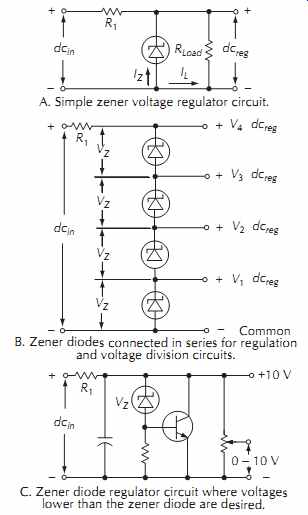
FIG. 10. Various regulator circuits using zener diodes.
4.2 Complex Power Supplies
Complex supplies include a pass element, a sampling element, and a comparator element, and they may include a preregulator, current limiting, undervoltage and overvoltage protection, and remote sensing.
Pass Elements. A transistor or group of transistors connected in parallel and placed in series with the output of a regulated power supply to control the flow of the output current. A pass element is another name for control element.
Reference Elements. The unit that forms the foundation of all voltage regulators. The output of the regulated power supply is equal to or a multiple of the reference. Any variation in the reference voltage will cause the output voltage to vary; therefore, the reference voltage must be maintained as stable as possible.
Sampling Elements. The device that monitors the output voltage and translates it into a level comparable to the reference voltage. The variations in the sampling voltage versus the reference voltage is the error voltage that ultimately controls the regulator output.
Comparator Elements. Compares the feedback voltage from the sampling element with the reference and provides gain for the detected error level. This signal controls the control circuit.
Preregulator. Monitors the voltage across the series regulator and adjusts the input Vin to maintain the regulator voltage at approximately 3 volts. This regulator voltage is held relatively constant regardless of input or output conditions. This reduces the power dissipated and the number of transistors in the series regulator, Fig. 11.
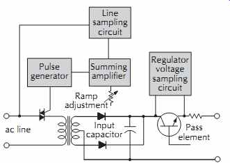
FIG. 11. Simplified block diagram of a pre-regulated power supply.
Current Limiting. A method used to protect the pass transistor by limiting the current within the safe operating range. The simplest current-limiting device is a resistor in series with the load. This, however, affects regulation by the IR drop across the resistor.
To overcome this, constant current limiting is used.
With constant current limiting, the voltage drop across the series resistor is sampled. The output voltage remains constant up to a predetermined current at which time the voltage decreases to limit the output current.
A third current limiting is foldback current limiting in which the load current actually decreases as the load continues to increase beyond Imax. This is usually only used in high current supplies.
The conventional current-limiting power supply of FIG. 12A is protected from instantaneous short circuits but long duration shorts can overheat Q2, leading to its eventual failure. In FIG. 12B this circuit is modified to produce foldback by adding two voltage feedback resistors, R3 and R4. The control transistor Q1 emitter voltage depends on the power supply output voltage as sampled by the R3, R4 voltage divider. If R1 senses a current overload, the drop across it decreases the output voltage and lowers the emitter voltage of Q1.
Then Q1 turns on at reduced current through R1, which limits current flow through Q2, as shown in the current foldback characteristic of FIG. 12B. The foldback ratio can be adjusted by changing R3, R4, or R1, or all three.
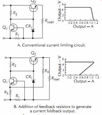
FIG. 12. Current limiting circuits.
Overvoltage Protection. Protects the load from over voltage. This may be accomplished internally or as an add-on to the power supply. A crowbar circuit is a typical overvoltage protector.
The circuit monitors the output voltage of a power supply and instantaneously throws a short circuit across the output terminals when a preset voltage is reached.
This is generally accomplished by the use of a silicon controlled rectifier (SCR) connected across the output terminals of the supply unit.
Remote Sensing. Adding two extra wires between the supply and the load produces a remote sensing circuit that permits the supply to achieve its optimum regulation at the load terminals, rather than at the power sup ply output terminals. In this manner, the circuit compensates for the IR drop in the line from the power supply to the equipment receiving its voltage. The sensing lines are high impedance and have almost no current flowing. Therefore, the voltage drop is negligible.
The wire size and voltage drop for regulated power supplies can be determined by Ohm's Law or with the use of the nomograph in Tables 14-2 and 14-3. Since regulated power supplies are designed to control the output at the power supply output terminals, the conductors used for the supply line must be considered as a part of the power supply load.
4.3 Switching Regulators
In a switching regulator, the pass transistor operates in an on-off mode, increasing efficiency and reducing heat.
The simple switching regulator shown in FIG. 13 incorporates a pulse generator circuit that pulses on the pass transistor as the output voltage decreases. As the output voltage increases, the comparator circuit reduces the pulse generator, reducing the on time of the pass transistor and, therefore, reducing the average output voltage. Since the output voltage is a series of pulses, a filter is required to smooth the dc output. An inductance-capacitance filter is commonly used. Switching regulators normally operate at 20 kHz or higher and have the following advantages:
• Switching regulators are on-off devices, so they avoid the higher power dissipation associated with the rheostat like action of a series regulator. Transistors dissipate very little power when either saturated (on) or nonconducting (off); most of the power losses occur elsewhere in the supply. Efficiency to 85% is typical for switching supplies, as compared to 30-45% for linear supplies. Less wasted power means switching supplies run cooler, cost less to operate, and have smaller regulator heat sinks.
• Size and weight reductions for switching supplies are achieved because of their high switching rate. Typically, a switching supply is less than one-third the size and weight of a comparable series-regulated supply.
• Switching supplies can operate under low ac input voltage (brownout) conditions and sustain a relatively long carryover (or holdup) of its output if input power is lost momentarily because more energy is stored in its input filter capacitors. In a switching supply, the input ac voltage is rectified directly, and the filter capacitor charges to the ac voltage peaks.
The ac voltage input of the standard linear supply is stepped down through a power transformer and then rectified, resulting in a lower voltage across its filter capacitor. Since the energy stored in a capacitor is proportional to CV2 and V is higher in switching supplies, their storage capability (and thus their holdup time) is better.
Switching disadvantages include the following:
• A switching supply transient recovery time (dynamic load regulation) is slower than that of a series-regulated supply. In a linear supply, recovery time is limited only by the speeds of the semiconductors used in the series regulator and control circuitry. In a switching supply, recovery is limited mainly by the inductance in the output filter.
• Electromagnetic interference (emi) is a natural by product of the on-off switching. This interference can be conducted to the load (resulting in higher output ripple and noise), it can be conducted back into the ac line, and it can be radiated into the surrounding atmosphere.
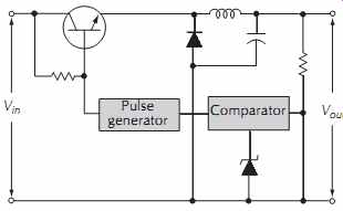
FIG. 13. Basic switching regulator.
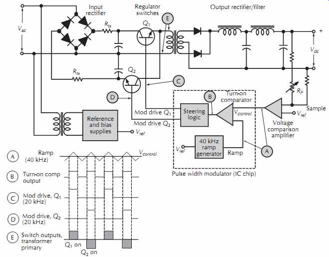
FIG. 14. Switching supply with push-pull transistors and feedback for regulation.
High-Power Regulated Supply.
Regulation of a high-power switching regulator is accomplished by push-pull switching transistors operating under control of a feed back network consisting of a pulse-width modulator and a voltage comparison amplifier, FIG. 14. The feed back elements control the on periods of the switching transistors to adjust the duty cycle of the bipolar wave form (E) delivered to the output rectifier filter. Here the waveform is rectified and averaged to provide a dc output level that is proportional to the duty cycle of the waveform, varying the on times of the switches.
The waveforms of FIG. 14 provide a more detailed picture of circuit operation. The voltage comparison amplifier continuously compares a fraction of the output voltage with a stable reference voltage, Vref, , to produce the Vcontrol level for the turn-on comparator. This device compares the Vcontrol input with a triangular ramp waveform A, occurring at a fixed 40 kHz rate. When the ramp voltage is more positive than the control level, a turn-on signal (B) is generated. Notice that an increase or decrease in the Vcontrol voltage varies the width of the output pulses at B and thus the on time of the switches.
Steering logic within the modulator chip causes switching transistors Q1 and Q2 to turn on alternately so that each switch operates at one-half the ramp frequency or 20 kHz.
The addition of a triac preregulator and associated control circuit improves regulation and ripple. The triac is a bidirectional device and is usually connected in series with one side of the input primary. Whenever a gating pulse is received, the triac conducts current in a direction that is dependent on the polarity of the voltage across it. The goal is to control the triac so that the bridge rectifier output (dc input to the switches) is held relatively constant. This is accomplished by a control circuit that issues a phase-adjusted firing pulse to the triac once during each half-cycle of the input ac. The control circuit compares a ramp function to a rectified ac sine wave to compute the proper firing time for the triac.
Although the addition of the preregulator circuitry increases complexity, it provides three important benefits:
1. By keeping the dc input to the switches constant, it permits the use of more readily available lower voltage switching transistors.
2. The coarse preregulation it provides allows the main regulator to achieve a finer regulation.
3. Through the use of slow-start circuits, the initial conduction of the triac is controlled, providing an effective means of limiting input surge current.
4.4 Phase-Controlled Regulated Power Supplies
In the phase-controlled supply, the pass element is switched on and off at line frequency and controls the output voltage by a varying pulse width. This is most often accomplished by using an SCR as the pass element. By delaying the firing point of the SCR1 in each cycle, the output voltage can be varied, FIG. 15.
SCR1 is fired by applying a voltage to the gate. The voltage is obtained by C1 charging through R2 and the ballast lamp. When the gate firing voltage is reached across C1, SCR1 fires. Once the SCR1 is on, it remains on until its anode voltage goes to zero, which is during the second half of the cycle. When SCR1 is on, C1 discharges and remains discharged until the phase of the line voltage returns to zero. The rate that the C1 charges is controlled by Q1. When Q1 is turned on, much of the C1 charging current is shunted around C1, requiring a longer time to charge C1, thus delaying the firing of SCR1. As the line voltage increases, the resistance of VDR1 and VDR2 decreases, turning Q1 on more and thus slowing the charging rate of C1. Since the output is a series of pulses with a high rise time of the leading edge, a filter is required on the output to smooth the dc.
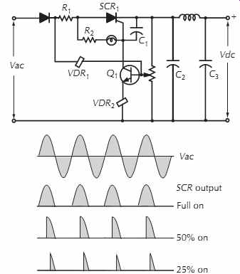
FIG. 15. Phase controlled regulated supply.
5. Single IC, Power Factor Corrected, Off-Line Supply
Many off-line power supplies now include power factor correction (PFC) which reduces input current and meets regulatory requirements.
1 Normal switching power sup plies that incorporate a bridge rectifier followed by bulk capacitance create harmonic currents, increasing the sup ply's rms input current, while contributing nothing to real power. To solve this problem a PFC preregulator and a separate controller was added to an existing design.
The Linear Technology Corporation LT1508 (voltage mode) and LT1509 (current mode) power supply eliminate combine the PFC and a pulse width modulator (PWM) function in a single 20-pin IC.
PFC is achieved by programming the input current of a boost regulator to follow the input line voltage, resulting in a near-unity power factor compared to 0.5-to 0.7 for a typical capacitive input switcher. The architecture maintains 0.99 power factor over a 20:1 load range. Start-up is controlled by separate PFC and PWM soft start pins. The PWM Soft Start pin is held low, disabling the PWM output until the PFC stage is in regulation. The PWM will remain enabled as long as the PFC output voltage stays above 73% of its preset value (typically 280 V out of 383 V for universal input). A separate overvoltage protection pin can be connected to the output through an independent resistor divider. This ensures overvoltage protection during safety agency abnormal testing conditions, such as opening the main feedback path. The two stages are synchronized and the PWM turn-on is delayed for 50% of the oscillator cycle.
This minimizes noise and conducted emission problems. 2 A peak current gate drivers and a 1.2 V optoisolator offset on the VC pin further simplify the design.
A universal input, 24 Vdc, 300 W converter using the LT1508 is shown in FIG. 16. Following the PFC boost preregulator is a 2-transistor forward converter that features low voltage (500 Vdc) switches, low peak currents and automatic non-dissipative core reset. Under worst case conditions (low line, full power), the PFC and PWM stages have efficiencies of 90% and 92% respectively. The LT1508's low start-up current of 250 PA minimizes start-up resistor power dissipation.
An overwinding on T1 provides the bootstrapped chip supply. The intermediate bus voltage of 382 V is well controlled, simplifying the post regulator and increasing capacitor holdup time compared to a typical off-line converter.
6. Synchronous Rectification Low-Voltage Power Supplies
Synchronous rectifiers can improve switching-power supply efficiency, particularly in low-voltage low-power applications compared to Schottky-diode types of supplies.
A synchronous rectifier is an electronic switch that improves power-conversion efficiency by placing a low resistance conduction path across the diode rectifier in a switch-mode regulator. MOSFETs or bipolar transistors and other semiconductor switches can be used.
The forward-voltage drop across a switch-mode rectifier is in series with the output voltage, so losses in the rectifier determine efficiency.
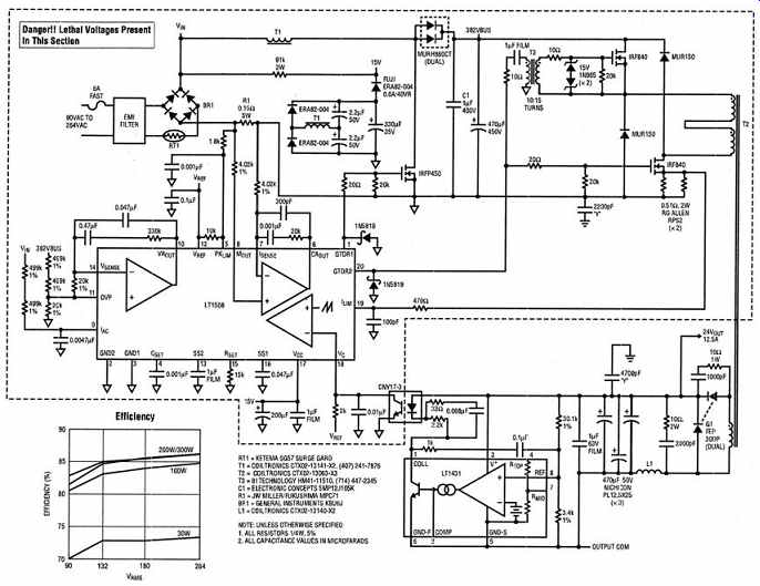
FIG. 16. 24 V, 300 W off-line PFC supply. Courtesy Linear Technology
Corporation.
Even at 3.3 V, rectifier loss is significant. For step down regulators with a 3.3 V output and a 12 V input, the 0.4 V forward voltage of a Schottky diode represents a typical efficiency penalty of about 12%. The losses are less at lower input voltages because the rectifier has a lower duty cycle and thus a shorter conduction time. However, the Schottky rectifier's forward drop is usually the dominant loss mechanism.
For an input voltage of 7.2 V and an output of 3.3 V, a synchronous rectifier improves on the Schottky diode rectifier's efficiency by around 4%. As output voltage decreases, the synchronous rectifier provides even larger gains in efficiency, FIG. 17.
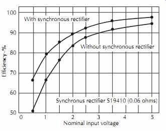
FIG. 17. Data based on a high-performance buck switch-mode regulator
and powered from a standard 7.2 V notebook-computer battery shows that the
synchronous rectifier has little effect on efficiency at 5 V, but offers significant
improvements at 3.3 V and below. Courtesy Maxim Integrated Products.
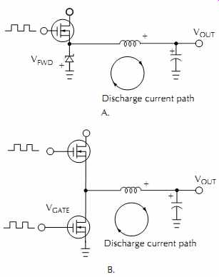
FIG. 18. A synchronous rectifier replaces the Schottky diode in A with
a low RDS(ON) MOSFET in B. The lower-resistance conduction path improves efficiency
for the 5-3.3 V 3 A converter by 3-4%. Maxim Integrated Products.