The field-effect transistor (FET) exhibits high input impedance (in the megohms) and accordingly presents negligible loading to a signal source or preceding stage. In this respect, the FET, unlike the conventional bipolar transistor, behaves more like a vacuum tube than a semiconductor device. FET transconductance is high (1000 to 12,000 micromhos, depending upon make and model) and maximum operating frequency likewise is high (up to 500 MHz for some types). This device is useful in all kinds of electronic circuits and can directly replace the tube in some of them.
The kind of FET featured in this section is the junction type (JFET). It is composed of junctions in a silicon chip, but is quite different from a junction-type bipolar transistor, as is explained below.
Before working with FETs. read the hints and precautions in section 1.
FET THEORY
Figure 2-1 (A) shows the cross section of a FET. A manufactured unit is somewhat more complex in structure, but the illustration given here is functionally correct and will demonstrate the basic structure and behavior of the device. In this FET. P-regions are processed into opposite faces of an N-type chip and are connected together to form the control electrode (called the gate. G) which corresponds to the grid of a tube or the base of a bipolar transistor.
An ohmic connection is made at each of the two ends of the chip. One of these is termed the drain (D) and corresponds to the plate of a tube or the collector of a bipolar transistor, and the other is termed the source (S) and corresponds to the cathode of a tube or the emitter of a bipolar transistor. The region extending internally from drain to source and passing between the two halves of the gate electrode is termed the channel.
Although Fig. 2-1 (A) shows P-type gate electrodes in an N-type chip, the opposite arrangement also is possible; that is, N-type gate electrodes can be processed into a P-type chip. An FET employing an N-type chip is termed an N-channel FET or an NFET, and its circuit symbol appears in Fig. 2-1 (B), whereas a FET employing a P-type chip is termed a P-channel FET or a PFET, and its circuit symbol appears in Fig. 2-1 (C).
Figure 2-2 illustrates FET operation. Here, a DC supply (Vdd) provides operating voltage (Vds) between drain and source, with drain positive and source negative; and a second DC supply (Vgg ) provides a bias voltage (Vgs ) between gate and source, with gate negative and source positive. In Fig. 2-2 (A), the gate voltage is zero, and under this condition, a maximum value of drain current (ID ) flows from supply Vdd , through the channel, and back to Vdd . In Fig. 2-2 (B), the gate voltage has a low negative value.
The application of this voltage causes a depletion layer-a region in which no current carriers exist-to appear around each of the P-regions of the gate electrode, as shown by the dotted lines. These layers penetrate deep into the chip and narrow the channel, thereby reducing drain current ID. When the gate voltage is increased to a sufficiently high negative value, the depletion layers meet and block the channel, cutting off the flow of drain current.
Between these limits of maximum current and cutoff, the drain current may be set to any intermediate value by appropriately setting the gate voltage. Because the drain current is controlled by gate voltage, the FET possesses transconductance and is a good amplifier. And because the control (gate) electrode is a reverse biased PN junction, any control current is negligible; that is. the input resistance of the device is very high. Figure 2-2 (C) shows FET performance in a family of curves resembling those for a pentode tube. An NFET is shown in Fig. 2-2; for a PFET, reverse the polarity of Vdd and Vgg . The performance curves will remain substantially the same as in Fig. 2-2 (C).
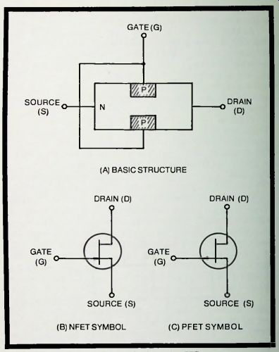
Fig. 2-1. Details of junction FET. (A) BASIC STRUCTURE (C) P-FET SYMBOL (B) N-FET
SYMBOL.
AUDIO PREAMPLIFIER
The FET is admirably suited to miniature AF amplifiers because it is small, it possesses high input impedance, it needs only a small amount of DC power, and it provides good frequency response. Such AF amplifiers, employing simple …
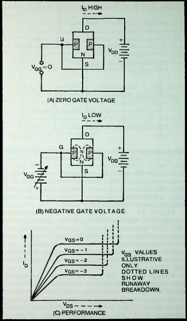
Fig. 2-2. JFET action.
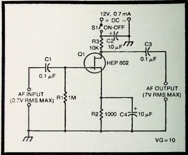
Fig. 2-3. Single-stage AF preamplifier.
… circuits, provide good voltage gain and may be built tiny enough to be contained in a microphone handle or in an AF test probe. They are easily inserted also into other equipment at points where a signal boost is needed and where existing circuitry must not be appreciably loaded.
Figure 2-3 shows the circuit of a single-stage, one-transistor amplifier offering all the advantages of the FET. This is a common-source circuit, equivalent to the common-cathode tube circuit and common-emitter bi-polar-transistor circuit. The input impedance of the amplifier is approximately the 1 megohm presented by resistor R1. The HEP 802 is an inexpensive and easily obtained PET, Voltage gain of the amplifier is 10. The maximum input-output amplitude before output-signal peak clipping is approximately 0.7 volt rms, and the corresponding output-voltage amplitude is 7 volt rms. At full operation, the circuit draws 0.7 mA from the 12-volt DC supply. With an individual FET. the input-signal voltage, output-signal voltage and DC operating current may differ somewhat from the values given above. Between 100 Hz and 25 kHz, the frequency response of the circuit is within 1 dB of the 1000 Hz reference.
All resistors are 1/4- or 1/2-watt. Electrolytic capacitors C2 and C4 are 35-volt units, and capacitors C1 and C3 may be any convenient low-voltage units. Any type of battery or other DC power supply can be used; the amplifier may even be sun powered by two type SP4C4OB silicon solar modules connected in series. If desired, continuously variable gain control may be obtained by substituting a 1-megohm potentiometer for resistor R1.
This circuit is suitable as a preamplifier or as a main amplifier in all applications requiring a 20 dB signal boost throughout the audio spectrum. The high input impedance and medium output impedance will satisfy most requirements. For very low-noise applications, the HEP 802 may be replaced with a 2N3578; however, the latter is a P-channel FET and will demand reversal of the DC supply.
------
TWO-STAGE AF AMPLIFIER
Figure 2-4 shows the circuit of a two-stage FET amplifier consisting of two identical RC-coupled stages of the type discussed in the previous section. This unit will give a substantial boost (40 dB) to a small AF signal, and can be used either alone or as a stage in other equipment. The HEP 802 transistors are low-priced and readily available. The input impedance of the amplifier is approximately 1 megohm, the resistance of the input-stage resistor, R1.
Overall voltage gain of the amplifier is 100. but this figure may vary somewhat-up or down-with individual FETs. The maximum input-signal amplitude before output-signal peak clipping is 70 mV rms. and the corresponding output-signal amplitude is 7 volts rms. At full operation, the circuit draws approximately 1.4 mA from the 12-volt DC supply, but this current may vary a small amount with individual FETs. (No need was found for a decoupling filter between stages, and such a filter will decrease the current of one stage.) The frequency response of the amplifier is flat within ± 1 dB of the 1 kHz level, from 100 Hz to better than 20 kHz.
All resistors in the circuit are 1/4- or 1/2-watt. Electrolytic capacitors C2, C4, and C6 are 25-volt units, and capacitors C1, C3, and C5 may be any convenient low-voltage units. The amplifier can be operated from a self-contained 12-volt battery or from an external battery or line-operated power supply.
Since the input stage runs "wide open,'' there may be some tendency to pick up hum and noise unless this stage and the input leads are well shielded. In stubborn cases, R1 may be reduced to 0.47 Meg. Where the amplifier must introduce only small loading of the signal source, R1 may be increased to as a high a value as 22 megohms, provided the input stage is very well shielded. However, resistance higher than this value tends to approach the FET junction resistance. For very low noise applications, the input HEP 802 FET (QI) may be replaced with a 2N3578; however, the latter is a P-channel FET and will demand reversal of the DC supply.
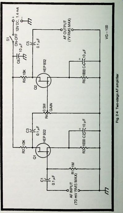
Fig. 2-4
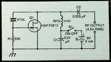
Fig. 2-5. Untuned crystal oscillator.
UNTUNED CRYSTAL OSCILLATOR
A Pierce-type crystal oscillator has the advantage that it requires no tuning; plug in the crystal, switch on the DC supply, and obtain RF output. A circuit of this type, employing a single HEP F0015 field-effect transistor, is shown in Fig. 2-5.
The untuned crystal oscillator finds use in transmitters, markers, receiver front ends, clock generators, crystal testers. RF signal generators, signal spotters (secondary frequency standards), and many similar devices. With most crystals, the circuit is a quick starter that is easy on crystals.
The untuned oscillator draws approximately 2 mA from the 6-volt DC supply. At this supply voltage, the open-circuit RF Output voltage is approximately 4.5 volts rms. DC supply voltages up to 12 volts can be used, with proportionately higher RF output.
To determine if the oscillator is operating, close switch S1 and connect an RF voltmeter to the RF Output terminals. (A high-resistance DC voltmeter shunted by a general-purpose germanium diode will suffice if an electronic voltmeter with RF probe is not available.) Deflection of the meter indicates oscillation. Alternatively, the oscillator may be connected to the Antenna and Ground terminals of a CW receiver which may be tuned through the crystal frequency to detect oscillation.
To prevent erroneous operation, the user must remember that the Pierce oscillator operates at the labeled frequency of a crystal only when the crystal is a fundamental-frequency cut. When overtone crystals are used, the oscillator output will not be the labeled frequency, but the lower frequency determined by the crystal dimensions. For operation at the labeled frequency of an overtone crystal, the oscillator must be of the tuned type.
TUNED CRYSTAL OSCILLATOR
Figure 2-6 (A) shows the circuit of a general-purpose crystal oscillator which will operate with all types of crystals.
The FET is an inexpensive and readily available HEP 801. The circuit is tuned by means of the screwdriver-adjusted slug in inductor LI. This oscillator is readily adapted to communications, instrumentation, and control applications. It may even be used as a flea-powered transmitter (DC power input. 12 mW) for communications or radio model control.
When the resonant circuit, L1-C1, is tuned to the crystal frequency, the oscillator draws approximately 2 mA from the 6-volt DC supply. The corresponding open-circuit RF output voltage is approximately 4 volts rms. (DC and RF values both will vary somewhat with individual FETs.) The drain current is lower on 100 kHz than on other bands, owing to the resistance of the inductor used for that frequency.
Figure 2-6 (B) lists commercial, slug-tuned inductors (LI) that can be used in this oscillator. Inductances have been chosen for the 100 kHz standard frequency, five ham radio bands, and the 27 MHz citizens' band; however, and appreciable inductance range is covered by adjustment of the slug of each inductor, and a wider frequency range than each band indicated in the table can be obtained with each inductor.
The oscillator may be tuned to a crystal frequency by adjusting the slug of the corresponding inductor (L1) for maximum deflection of an RF voltmeter connected to the RF Output terminals. (If an electronic voltmeter with an RF probe is not available, a high-resistance DC voltmeter shunted by a general-purpose germanium diode will suffice.) Alternatively, the oscillator may be tuned with a 0-5 DC milliammeter inserted temporarily at point X: Adjust the slug of inductor L1 for deepest dip in the meter reading.
All resistors are 0.25- or 1/2-watt. For best results, especially at the higher frequencies, the capacitors all should be of the mica type; for low frequency drift, C2 should be silvered mica.
The slug tuning arrangement provides fine-tuned operation. In applications where it is necessary to tune the oscillator continuously with a resettable dial, a 100 pF variable...
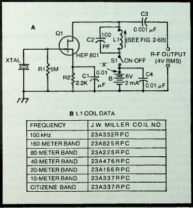
Fig. 2-6. Tuned crystal oscillator.
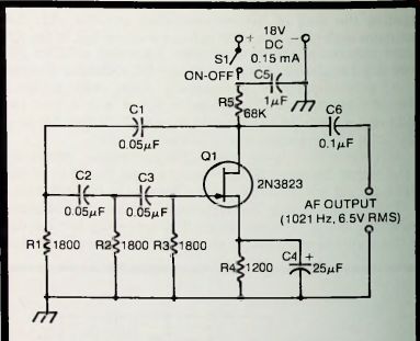
Fig. 2-7. Phase-shift audio oscillator.
...capacitor may be used in place of C2, and the slug employed only to set the top frequency of a tuning range.
PHASE-SHIFT AUDIO OSCILLATOR
The phase-shift oscillator is a relatively simple resistance-capacitance tuned circuit which is prized for its clean output signal (low-distortion sine wave). The field-effect transistor is well suited to this circuit, since the high input impedance of this semiconductor device results in virtually no loading of the frequency-determining RC network.
Figure 2-7 shows the circuit of a phase-shift AF oscillator employing a single FET. In this circuit, the frequency is determined by the three-leg RC phase-shift network (C1-C2-C3-R1-R2-R3) from which the oscillator takes its name.
For the necessary 180° phase shift for oscillation in the feedback path between the drain and gate of FET Q1, the R and C values in the network are selected for 60° shift in each leg (R1-C1, R2-C2, and R3-C3). For simplicity, the capacitances are kept equal ( C1 = C2 = C3) and the resistances are kept equal (R1 = R2 = R3). The frequency of the network (and accordingly the oscillation frequency of the circuit) then is f = 1/ (10.88 RC). where f is in hertz, R in ohms, and C in farads. With the network values given in Fig. 2-7, the frequency therefore is 1021 Hz (for exactly 1000 Hz with the 0.05 u-F capacitors, R1, R2, and R3 each must be 1838 ohms). When experimenting with a phase-shift oscillator, it will be easier to work with the resistors than with the capacitors. For an available capacitance (C), the required resistance (R) for a desired frequency (f) is R = 1/(10.88 f C), where R is in ohms, f in hertz, and C in farads. Thus, with the 0.05 u-F capacitors shown in Fig. 2-7, the resistance required for 400 Hz = 1/(10.88 x 400 X 5 X 10^8 ) = 1/0.0002176 = 4596 ohms.
The 2N3823 FET provides the high transconductance (6500 u-mho) required for good operation of a phase-shift oscillator. The circuit draws approximately 0.15 mA from the 18-volt DC supply, and the open-circuit AF output is approximately 6.5 volts rms. (The DC and AF values both will vary somewhat with individual FETs.)
All resistors in the circuit are or 1/4-watt. Capacitors C5 and C6 can be any convenient low-voltage units. Electrolytic capacitor C4 is a 25-volt unit. For frequency stability, capacitors C1, C2, and C3 must be of top quality and closely matched in capacitance.
PRODUCT DETECTOR
Figure 2-8 shows the circuit of a simple product detector employing a HEP F0015 field-effect transistor. This detector is easily included in compact receiver circuits for CW and SSB reception. Here, the output of the IF amplifier is applied to the gate of the FET. and the output of the beat-frequency oscillator (BFO) is applied to the source across unbypassed source resistor R4. The IF and BFO signals are mixed and produce an AF signal in the drain output circuit of the FET. A pi-type low-pass filter (C4-C5-RFC1) removes the intermediate frequency from the audio output of the detector (a suitable 91-mH RF choke for use in this filter is J. W. Miller No. 70F912AF, having an internal resistance of 250 ohms).
The circuit draws approximately 1 mA from the 18-volt DC supply which may be obtained from any convenient point in the receiver, but this current will vary somewhat with individual FETs. The AF output amplitude will depend upon the relative amplitudes of the IF and BFO signal voltages. For low-distortion operation, i.e.. linear detection, it is recommended that the amplitude of the BFO signal be not less than five times that of the IF signal. Ideally, there is no output unless the IF and BFO signals are both applied. The resulting output signal is the product of the two input signals, hence the name product detector.
----
In construction, the IF and BFO input sections of the detector should be kept as clear of each other as practicable, to minimize stray coupling; shielding is advisable. Electrolytic capacitors C2 and C3 are rated at 35 volts or higher; capacitors C1, C4, and C5 are mica or good-grade ceramic units; and capacitor C6 may be any convenient low-voltage unit. All resistors are 0.25-or 0.5-watt.
----
ALL-WAVE REGENERATIVE RECEIVER
The regenerative receiver is a perennial favorite of radio experimenters. A reasonably sensitive device, it has a simple circuit and is easy to operate. It works over a wide frequency range and responds to either modulated or continuous-wave signals, and for a long time was the only receiver used by many radio hams and short-wave listeners. As an emergency receiver, the regenerative set can be quickly assembled at low cost.
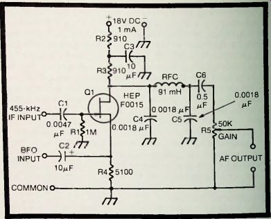
Fig. 2-8. Product detector.
---
Figure 2-9 shows the circuit of a tickler-coil type of regenerative receiver which covers the frequency range 440 kHz to 30 MHz in five overlapping bands: 440-1200 kHz, 1-3.5 MHz. 3.4-9 MHz. 8-20 MHz. and 18-30 MHz. Plug-in coils provide a separate tuning inductor (L1) and tickler (L2) for each band. The single FET is an inexpensive HEP 802. In this circuit, positive (regenerative) feedback is obtained by inductively coupling energy back from the drain output circuit of the FET to the gate input circuit via the coupling between tickler coil L2 and tuning coil L1.
The regeneration control is the 50K wirewound potentiometer, R2, by means of which the DC drain voltage is adjusted. At the highest-voltage setting of R2, the circuit will break into oscillation. A pi-type filter (RFC-C4-C5) removes the RF component from the output circuit. Resistor R1 is a 1/4- or 1/2-watt unit, and capacitors C3, C4, C5, and C6 should be mica or good-grade ceramic units.
The audio-frequency output signal is coupled from the circuit by transformer T. This may be any convenient interstage coupling transformer, preferably having a secondary-to-primary turns ratio of 1:1. 2:1, or 3:1. The receiver may be coupled to an audio amplifier, or high-impedance headphones may be connected directly to the AF output terminals.
Table 2-1 gives specifications and winding instructions for the plug-in coils. These coils are wound on 1-inch diameter 4-pin plastic forms and are plugged into a 4-contact socket.
---------------------
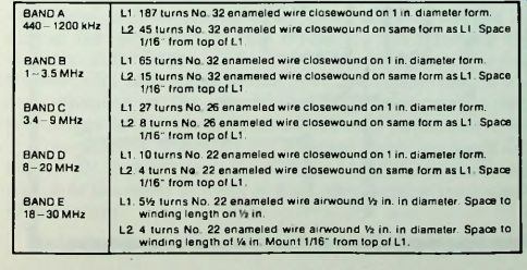
Table 2-1. Coil-Winding Data For All-Wave Regenerative Receiver
27 BAND D 8-20 MHz BANDA 440-1200 kHz BANDC 3.4 -9 MHz BANDE 18-30MHZ BANDS 1-3.5 MHz
L1. 187 turns No. 32 enameled wire closewound on 1 in. diameter form.
L2. 45 turns No. 32 enameled wire closewound on same form as Li. Space 1/16" from top of L1.
L1.65 turns No. 32 enameled wire closewound on 1 in. diameter form.
L2. 15 turns No 32 enameled wire closewound on same form as L1. Space 1/16" from top of L1.
L1.27 turns No 26 enameled wire closewound on 1 in. diameter form.
L2. 8 turns No 26 enameled wire closewound on same form as L1. Space 1/16" from top of L1.
L1.10 turns No. 22 enameled wire closewound on 1 in. diameter form.
L2. 4 turns No 22 enameled wire closewound on same form as L1 Space 1/16" from top of L1
L1. 5 1/2 turns No. 22 enameled wire air-wound 1/2 in. in diameter. Space to winding length on in.
L2. 4 turns No. 22 enameled wire air-wound V1 in. in diameter. Space to winding length of' 1/4 in. Mount 1/16" from top of L1.
----------------
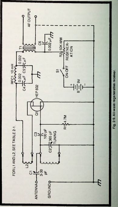
Fig. 2-9
To test the regenerative circuit initially:
1- Connect high-impedance headphones to AF output terminals,
2- Set potentiometer R2 to its lowest-voltage position.
3- Set tuning capacitor C2 to maximum capacitance.
4- Close switch S1.
5- Slowly advance setting of R2; as maximum-voltage setting is approached, circuit should break into oscillation evidenced by beat-note whistle in headphones. If oscillation fails to occur, reverse leads to L1 or L2, but not both.
6- Connect antenna and ground, adjust C2 to tune-in signals, and adjust R2 for maximum weak-signal sensitivity without causing sustained oscillation of receiver. With some FETs. it may be necessary to experiment with the resistance of R1 to obtain maximum sensitivity.
7-The 3-30 pF antenna coupling capacitor, C1, is a screwdriver-adjusted trimmer capacitor. Set this trimmer for minimum capacitance that will give a strong signal. The adjustment should be optimum for all five frequency bands, so that C1 need not be readjusted.
The receiver tuning may be calibrated with the aid of an AM signal generator connected to the antenna and ground terminals. For this purpose, connect high-impedance headphones or AF voltmeter to AF output terminals, and at each setting of the signal generator, tune C2 for audio peak and inscribe the frequency on the C2 dial. The top frequency in each band may be placed at the same point on the dial by setting the generator to that frequency and adjusting the trimmer on the frame of C2 (most 365 pF capacitors have this trimmer) for audio peak at that point. No volume control has been included in the circuit; but if it is desired, a 50K potentiometer may easily be added at the AF output terminals.
The current drawn by the receiver from the 9-volt DC source (B) depends upon the setting of potentiometer R2 and will be of the order of 1 mA at the highest setting (maximum regeneration).
--------------
SUPERREGENERATIVE RECEIVER
For its small size, low cost, and simplicity, the superregenerative detector has no equal in sensitivity to signals. Especially useful at ultra-high frequencies, the super-regenerator is broad enough in response to "hold onto" a floppy signal, and it has a built-in AGC action.
Figure 2-10 shows the circuit of a self-quenching type of superregenerative receiver built around a 2N3823 VHF field-effect transistor. With four coils, the circuit covers the 2-, 6-. and 10-meter ham bands and the 27 MHz region (see Table 2-2). The frequency coverage allows the receiver to be used for general communications and for radio model control. All coils are single, two-terminal units. The 27 MHz and 6- and 10-meter coils are commercial, slug-tuned units which must be mounted on two-pin plugs for easy insertion and removal (for single-band receivers, these coils may be soldered permanently into the circuit). However, the 2-meter coil must be wound by the reader, and it too must be provided with a plug-in base, except in a single-band receiver. A filter system (RFC1-C5-R3) removes the RF component from the receiver output circuit, and a second filter (R4-C6) attenuates the quench frequency. A suitable 2.4 uH inductor for the RF filter is J. W. Miller No. 4406.
------------------
Table 2-2. Coil Data For Superregenerative Receiver
TUNING
Capacitance = 15 pF
A. 10-Meter Amateur Band. J. W Miller No. 4405. Adjust core.
B. 6-Meter Amateur Band. J. W. Miller No. 4403. Adjust core.
C. 2-Meter Amateur Band 4 turns No. 14 bare wire air-wound 1/2 in. in diameter. Space to hit band.
D. 27- MHz Range. J. W Miller No. 4405. Adjust core.
------------------
To test the superregenerative circuit initially:
1- Connect high-impedance headphones to AF output terminals.
2- Set volume-control potentiometer R5 to its maximum-output position.
3- Set regeneration-control potentiometer R2 to its bottom end.
4- Set tuning capacitor C3 to maximum capacitance.
5- Close switch S.
6- Advance setting of potentiometer R2. noting that at one setting a loud hiss begins, marking the onset of superregeneration. Loudness of this hiss should be fairly uniform as capacitor C3 is varied, but should increase somewhat as R2 is advanced to the top of its setting.
7- Connect antenna and ground. If connection of antenna stops hiss, adjust antenna trimmer capacitor C1 to restore this. This trimmer is screwdriver adjusted and should need adjustment only once to accommodate all frequency bands.
8- Tune-in signals in each band, noting the AGC action of the receiver and the nasal quality of its voice reproduction.
9- The receiver tuning dial, attached to C3. may be calibrated with the aid of an AM signal generator connected to the antenna and ground terminals. Connect high-impedance headphones or AF voltmeter to AF output terminals, and at each setting of the generator, tune C3 for audio peak. The top frequency in the 10-meter, 6-meter, and 27 MHz bands may be placed at the same point on the C3 dial by adjusting the screw slugs in the corresponding coils, with the signal generator set to the appropriate frequency and with C3 set to the desired point near minimum capacitance. The 2-meter coil, however, has no slug and must be adjusted by squeezing or spreading its turns for alignment with the top-band frequency.
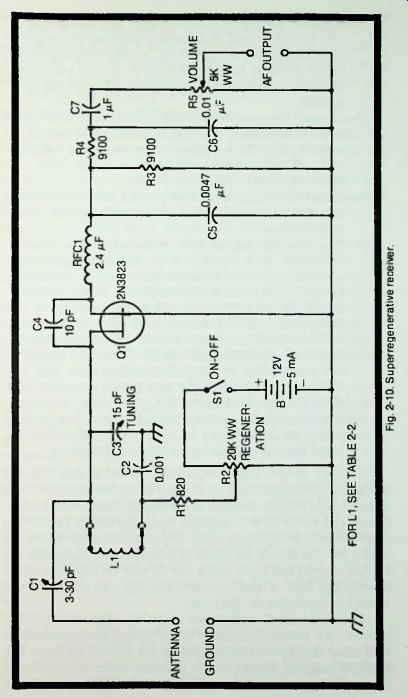
Fig. 2-10
Because of the high frequencies at which this receiver operates, particular care is needed in its construction. The shortest practicable straight leads must be used in the tuned circuit (L1-C1-C2-C3-R1), and the mounting of this part of the receiver must be firm and solid. Any subpanel employed in the tuning section should be made of polystyrene. Capacitors C2, C4, C5, and C6 are mica units, but C7 may be any convenient low-voltage unit. Fixed resistors R1, R3, and R4 are 1/4 or 1/2-watt composition or film units.
The user must remember that the superregenerative receiver is a notorious radiator of RF energy and can interfere with other nearby receivers tuned to the same frequency. The antenna coupling trimmer, C1, provides some attenuation of this radiation and so does reduction of the battery voltage to the lowest value that will still afford good sensitivity and audio volume. A radio-frequency amplifier operated ahead of the super-regenerator is a very effective medium for minimizing radiation; but at the frequencies at which the receiver operates, such an amplifier is not easily fabricated and it negates the simplicity of the super-regenerator.
ELECTRONIC DC VOLTMETER
Figure 2-11 shows the circuit of a balanced electronic DC voltmeter having an input resistance (including the 1-megohm resistor in the shielded probe) of 11 megohms. The circuit draws approximately 1.3 mA from a self-contained 9-volt battery, B, hence can be left running for extended periods.
This instrument covers 0-1000 volts in eight ranges: 0-0.5, 0-1, 0-5, 0-10, 0-50, 0-100,0-500, and 0-1000 volts.
In the input voltage divider (range switching), the required resistances are made up of series-connected stock-value resistors which must be selected carefully for resistance close to the indicated values. If precision instrument-type resistors are available, the number of resistors in this string can be halved. That is, for R2 and R3, substitute 5 Meg.; for R4 and R5, 4 Meg.; for R6 and R7, 500 K; for R8 and R9, 400 K; for R10 and R11, 50 K; for R12 and R13, 40K; for R14 and R15, 5 K; and for R16 and R17, 5K.
A balanced circuit such as this has virtually no zero drift; any drift in FET QI is balanced out automatically by a similar drift in Q2. The internal drain-to-source circuits of the FETs, in conjunction with resistors R20. R21. and R22, form a resistance bridge. Indicating microammeter M1 is the J detector in this bridge circuit. With zero signal input to the electronic voltmeter, meter M1 is set to zero by balancing this bridge with the aid of potentiometer R21. When a DC voltage subsequently is applied to the input terminals, the bridge unbalances-since the internal drain-to-source resistance of the FETs changes--and the meter deflects proportionately.
The RC filter formed by R18 and C1 removes AC hum and noise picked up by the probe and the voltage-switching circuits.
Initial Calibration
With zero voltage at the input terminals:
1-Close switch S2 and set potentiometer R21 to zero pointer of meter M1. Range switch S1 may be set to any position for this step.
2- Set range switch to its 1-volt position.
3- Connect an accurately known 1-volt DC source to input terminals.
4- Adjust calibration control R19 for exact full-scale deflection of meter Ml.
5- Temporarily remove input voltage and note if meter still is zeroed. If it is not, reset R21.
6- Work back and forth between steps 3, 4, and 5 until a 1-volt input deflects meter to full scale, and meter remains zeroed when input is removed.
Rheostat R19 will need no readjustment after this process unless its setting is disturbed or the instrument later needs recalibration. Zero-set potentiometer R21 will need only occasional resetting.
If range resistors R2 to R17 are accurate, this single-range calibration will be sufficient; all other ranges will automatically be in calibration. A special voltage card can be drawn for the meter, or the existing 0-100 uA scale may be read in volts by mentally applying the appropriate multiplier on all but the 0 -100 volt range.
-----------
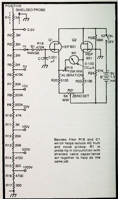
Fig. 2-11. Electronic DC voltmeter. Besides filter R18 and C1 which helps reduce
AC hum and noise pickup, R1 in probe tip in conjunction with shielded cable
capacitance act together to help do the same job.
-------------
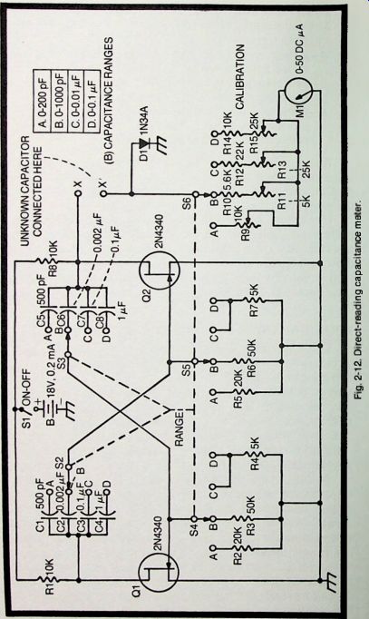
Fig. 2-12
DIRECT-READING CAPACITANCE METER
Quick, direct reading of capacitance is afforded by the circuit shown in Fig. 2-12. This instrument covers 0-0.1 u-F in four ranges: 0-200 uF, 0-1000 uF, 0-0.01 uF, and 0-0.1 uF. Operation of the circuit is linear, so the scale of the 0-50 DC microammeter. M1. can be graduated in picofarads and microfarads. An unknown capacitance connected to terminals X-X then may be read directly from the meter, without calculations or balancing adjustments. The circuit draws approximately 0.2 mA from a self-contained 18-volt battery, B.
In this circuit, the two FETs (Q and Q2) are operated in a conventional drain-coupled multivibrator. The multivibrator output, taken from the drain of Q2, is a constant-amplitude square wave whose frequency is determined principally by the values of capacitors C1 to C8 and resistors R2 to R7. On each test range, the selected capacitances are identical and so are the selected resistances. A 6-pole. 4-position. rotary switch (S1-S2-S3-S4-S5-S6) selects the correct multivibrator capacitors and resistors and the meter-circuit resistance combination required for the test frequency for a selected capacitance range. The square-wave output is coupled through the unknown capacitor (connected to terminals X-X) to the meter circuit (diode D1. one of the resistance legs selected by switch section S6. and 0-50 DC microammeter M1). No zero setting of the meter is needed; the pointer remains at zero until an unknown capacitor is connected to terminals X-X.
For a given square-wave frequency, the meter deflection is directly proportional to unknown capacitance C. and the meter response is linear. Thus, if in the initial calibration of the circuit an accurately known 1000 pF capacitor is connected to terminals X-X. the range switch is set to its position B, and calibration rheostat R11 is set for exact full-scale deflection of Ml. then the meter will indicate 1000 pF at full scale. Owing to its linear response, the meter will indicate 500 pF at half scale, 100 pF at 1/10 scale, and so on.
The multivibrator frequency is switched to the following values for the four capacitance ranges: 50 kHz (0-200 pF), 5 kHz (0-1000 pF), 1000 Hz (0-0.01 uF), and 100 Hz (0-0.1 mF). For this purpose, switch sections S2 and S3 switch the multivibrator capacitors in identical pairs at the same time that switch sections S4 and S5 switch the multivibrator resistors in identical pairs.
The frequency-determining capacitors must be capacitance-matched in pairs:
C1 = C5, C2 = C6, C3 = C7, and C4 = C8.
Likewise, the frequency-determining resistors must be resistance-matched in pairs:
R2 = R5, R3 = R6, and R4 = R7.
The drain load resistors, R1 and R8, also should be matched. The calibration rheostats--R9, R11, R13, and R15--must be wirewound units; and since they are adjusted only during calibration, they may be mounted inside the instrument case and provided with slotted shafts for screwdriver adjustment. All fixed resistors (R1 to R8, R10, R12, R14) must be 1-watt units.
Initial Calibration
For calibration, four accurately known, very-low-leakage capacitors will be required: 0.1 mF. 0.01 mF, 1000 pF, and 200 pF.
1- With the range switch in its position D, connect the 0.1 mF capacitor to terminals X-X.
2- Close switch S1.
3- Adjust calibration rheostat R15 for exact full-scale deflection of meter M1.
4- Open switch S1.
5- Connect the 0.01 uF capacitor to terminals X-X in place of the 0.1 uF unit.
6- Set the range switch to Position C.
7- Close switch S1.
8-Adjust calibration rheostat R13 for exact full-scale deflection of the meter.
9-Open switch S1.
10- Connect the 1000 pF capacitor in place of the 0.01 uF unit.
11-Set the range switch to position B.
12-Close switch S1.
13-Adjust calibration rheostat R11 for exact full-scale deflection of the meter.
14-Open switch S1.
15-Connect the 200 pF capacitor in place of the 1000 pF unit, using the shortest and straightest leads practicable.
16-Set the range switch to position A.
17-Close switch S1.
18-Adjust calibration rheostat R9 for exact full-scale deflection of the meter.
19-Open switch S1.
20-Disconnect the 200-pF capacitor from terminals X-X.
A special meter card may be drawn, or figures may be inscribed on the present microammeter scale to show capacitance ranges of 0-200 pF, 0-1000 pF, 0-0.01 uF, And 0-0 1 mF. In subsequent use of the instrument, it will be necessary only to connect an unknown capacitor to terminals X-X. close switch S1. and read the capacitance from the meter.
For best accuracy, use the range that will give the deflection in the upper part of the meter scale.