The metal oxide semiconductor field-effect transistor (MOSFET) is a special type of field-effect transistor in which the gate electrode is not the junction found in the conventional field-effect transistor (see section 2). but is a small metal plate insulated from the rest of the structure by a thin film of silicon dioxide. Any gate current in this device therefore is the leakage current of this insulation, and is as low as 10 pico-amperes (10" ampere) in some models. This gate gives the MOSFET extremely high input resistance, superior to that of the FET. This feature of the MOSFET is responsible for the alternate name of the device: insulated-gate field-effect transistor (IGFET).
MOSFETs are now available, as discrete units, in a wide variety of ratings and types. Before working with MOSFETs, read the hints and precautions in section 1. especially items 3. 10. and 19.
MOSFET THEORY
Figure 3-1 (A) shows the cross section of a MOSFET. Although this representation may not be the exact picture of a particular manufactured unit, it is functionally correct and will serve to illustrate the main differences between MOSFETs and conventional junction FETs. (The various regions shown in the substrate are not to scale.) The...
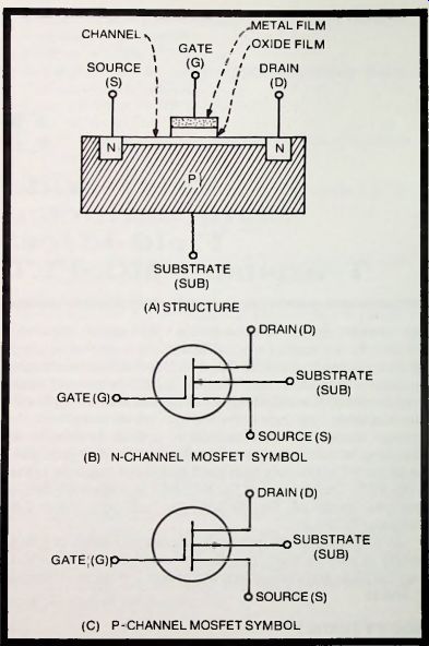
Fig. 3-1. Details of MOS field-effect transistor. (A) STRUCTURE (B) N-CHANNEL
MOSFET SYMBOL (C) P-CHANNEL MOSFET SYMBOL
...electrodes of the MOSFET are drain, D (corresponding to the plate of a tube or the collector of a bipolar transistor), source, S (corresponding to the cathode of a tube or the emitter of a bipolar transistor), and gate. G (corresponding to the grid of a tube or the base of a bipolar transistor). The drain and source consist of small N-regions processed into a P-type substrate.
Connecting the drain and source is a thin N-type channel lying just under the top face of the substrate. The metal gate electrode rests on the channel and is insulated from it by a very thin film of silicon dioxide (the insulating film is grown on the substrate, and the gate is deposited on the film).
This particular type of device is termed an N-channel MOSFET. and its circuit symbol is shown in Fig. 3-1 (B). If, instead of this structure, we have an N-type substrate, the drain, source, and channel are P type. The resulting device is termed a P-channel MOSFET. and its circuit symbol is shown in Fig. 3-1 (C). For the N-channel MOSFET. the external DC voltages are: drain positive, source negative. For the P-channel MOSFET. the voltages are: drain negative, source positive.
Figure 3-2 illustrates MOSFET operation. Here, a DC supply (VDd) provides an operating voltage (Vds) between drain and source, with drain positive and source negative; and a second DC supply (Vgg ) provides a bias voltage (Vgs ), with gate negative and source positive. The electric field of the gate penetrates the channel. Note that a gate-to-source resistor, R, is needed, since the gate insulation might be damaged if the gate floats.
In Fig. 3-2(A). the gate voltage is zero; and under this condition, a maximum value of drain current (ID ) flows from supply Vdd through the channel, and back to Vdd , since there is no field from the gate to affect current flowing through the channel. In Fig. 3-2(B). the gate voltage is negative; and the resulting field narrows the channel, reducing drain current ID. When the gate voltage is raised to a sufficiently high negative value, the channel is depleted completely and the drain current is cut off.
Between these limits of maximum and cutoff, the drain current may be set to any intermediate value by appropriately setting the gate voltage. Figure 3-2(C) shows MOSFET performance in a family of curves resembling those for a pentode tube. An N-channel MOSFET is shown in Fig. 3-2; for a P-channel MOSFET, reverse the polarity of VDD and Vgg .
Because the gate voltage acts to deplete the channel of current carriers, this type of MOSFET is termed depletion type. Other types are enhancement type and...
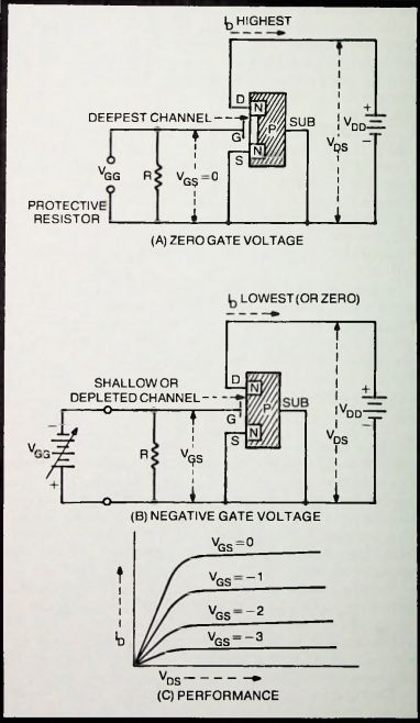
Fig. 3-2. MOSFET action.(A) ZERO GATE VOLTAGE (B) NEGATIVE GATE VOLTAGE; (C)
PERFORMANCE
...depletion/enhancement type, but are not described here because all units mentioned in this section are of the depletion type.
Because the drain current of the MOSFET is controlled by gate voltage, the MOSFET possesses transconductance (up to 15,000 u-mhos typical) and is a good amplifier. It also, like the tube and superior to the junction FET. has a very high input resistance (in some devices, up to 100 million megohms). Depending upon make and model, MOSFETs operate at frequencies up to 500 MHz.
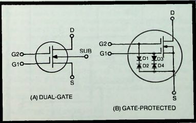
Fig. 3-3. Special MOSFETs (A) DUAL-GATE (B) GATE-PROTECTED
In addition to the single-gate MOSFET shown in Fig. 3-1 and 3-2. there are dual-gate units (see Fig. 3-3A). Also available is the gate-protected MOSFET (see Fig. 3-3B); in this type, internal, integrated back-to-back zener diodes (D1, D2, D3, D4) automatically protect the two gates from insulation damage resulting from static electric or excessive signal voltages. Single-gate, dual-gate, and gate-protected MOSFETs all are used in projects in this section.
GENERAL PURPOSE RF AMPLIFIER
Outrigger RF amplifiers are convenient as preselectors for boosting the sensitivity and selectivity of receivers. They also find use as signal boosters in electronic equipment other than receivers. The circuit shown in Fig. 3-4 may be used as an outrigger amplifier or as an RF amplifier stage which is built into an existing receiver or instrument. The circuit employs a 3N200 gate-protected MOSFET. a device which is operable to 400 MHz.
This is a standard tuned-gate, tuned-drain circuit; but, because of the low interelectrode capacitance of the 3N200, no neutralization is required. In this circuit, the incoming RF signal, selected by the input tuned circuit (L1-L2-C1) is presented to gate 1 of the MOSFET. The output signal is developed by drain current in the output tuned circuit (L3-L4-C5). Coaxial jacks (J1 and J2) or other suitable terminals permit easy input and output of the signal. The negative gate-1 bias is provided by the voltage drop resulting from the flow of drain current through source resistor R3.
Required positive gate-2 bias is produced by voltage divider R1-R2. With an individual MOSFET. resistor R2 may require some adjustment for maximum amplification.
Commercial plug-in coil sets with end links may be used when the amplifier must cover a wide tuning range. The per-section capacitance of the ganged tuning capacitor, C1-C5, then will be the value recommended by the coil manufacturer for the selected coils. When the amplifier is to be used exclusively in the standard broadcast band. L2 and L3 each must be 130 turns of No. 32 enameled wire closewound on a 1-inch diameter form. L1 will be 10 turns of No. 32 enameled wire closewound around the bottom end of L2, and L4 will be 12 turns of No. 32 enameled wire closewound around the bottom end of L3. These link-coupling coils ( L1 and L4) are insulated from the coils with which they are associated. For the broadcast band. C1 and C5 each will be 365 pF.
At frequencies much above the standard broadcast band, the amplifier circuit should be shielded. The unit may readily be built into an aluminum box. With shielded construction of this kind, there will be some advantage in using feed through capacitors for C2, C3, and C4.
DC operating voltage for the amplifier may be obtained from a self-contained battery (as B1 in Fig. 3-4) or from a well-filtered, power-line-operated supply. Current drain is approximately 5 mA, but this value can differ somewhat with an individual 3N200.
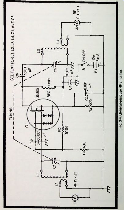
Fig. 3-4
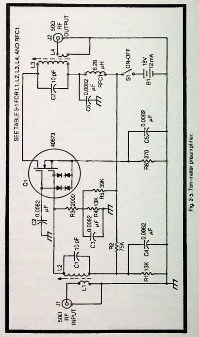
Fig. 3-5
TEN-METER PREAMPLIFIER
Figure 3-5 shows the circuit of a preamplifier (preselector) expressly for the 10-meter ham band. Employing permeability input and output tuning, this circuit is adapted from an original RCA design. Operation of the circuit is reasonably wide band, especially if input and output are stagger tuned, so that it can function as an aperiodic amplifier.

Table 3-1 gives coil data.
----------
A gate-protected 40673 MOSFET is used with dual bias to provide substantial signal boost. The DC bias on the signal gate (gate 1) is the combination of the negative voltage developed by the flow of drain current through source resistor R6 and the positive voltage developed by voltage divider R1-R2 (the net voltage at gate 1 is negative). The required positive voltage on gate 2 is developed by voltage divider R4-R5. With an individual MOSFET. resistors R2 and R5 may require some adjustment for maximum signal output.
The circuit is fix-tuned by means of the slug-adjusted coils, L2 and L3 (see Table 3-1). While, owing to the very low interelectrode capacitance of the 40673, no neutralization is required, the mechanical assembly must be arranged to keep the input and output soils well separated and preferably at right angles to each other. A very small amount of coupling between input and output will induce oscillation.
The input and output accommodate low antenna and receiver-input impedance. For a high-impedance antenna, connect the antenna to the top of L2 through a 10 pF capacitor.
Impedances other than 50 ohms may be accommodated by suitably changing the number of turns in L1 or 12.
All capacitors are silvered mica. All resistors are 1/2-watt. The circuit draws approximately 12 mA from the 12-volt DC supply which may be either battery (as B1 in Fig. 3-5) or a well-filtered power-line-operated supply.
The circuit may be aligned in the conventional manner, with a signal generator (tunable between the 28- and 29.7-MHz limits of the 10-meter band) connected to input jack J1, and a suitable indicator (such as an electronic RF voltmeter or the ...
---------------
Table 3-1. Coil Data For 10-M Preamplifier
L4 REC1 L1 L2 and L3
2 turns No 20 enameled wire closewound around ground end of L2.
Each subminiature, slug-tuned, ceramic-form coil. Inductance range 1.6 to 2.4 uH (J. W Miller No 4306) 2 turns No. 20 enameled wire closewound around ground (bottom)
end of L3.
6.28 uH microminiature RF choke. DC resistance 2 ohms (J. W Miller No. 9230-40).
-----------------------
... receiver itself into which the preamplifier is to operate) connected to output jack J2. Adjust the L2 and L3 slugs first for peak output at 28.8 MHz (approximate midband); then detune both input and output coils, one above this frequency and one below, for the desired bandwidth.
Also usable in this circuit are MOSFET types 3N187 and 3N200.
WIDEBAND INSTRUMENT AMPLIFIER
A video amplifier, such as shown in Fig. 3-6, exhibits wideband response, by operating from low audio frequencies well into the high radio frequencies. Such amplifiers are widely used in electronics, and are known mainly for their role in TV picture channels, oscilloscope horizontal and vertical channels, and sampling systems. The circuit in Fig. 3-6 is offered, however, especially as an instrument amplifier; that is. as a signal booster for oscilloscopes, electronic voltmeters, and other test instruments requiring an amplifier that needs no tuning. The MOSFET is a 40820. having high transconductance (12,000 u-mhos typical).
Frequency response of this circuit extends from 60 Hz to 10 MHz. The input impedance is approximately 1 Meg., determined principally by the resistance of the input resistor, R1. Output impedance is approximately 2800 ohms. These input and output values hold at 1000 Hz. The open-circuit voltage gain of the circuit is approximately 10 at 1000 Hz, and is down approximately 3 dB at 60 Hz and down approximately 6 dB at 10 MHz. The maximum input-signal voltage before output-signal peak clipping is approximately 100 mV rms, and the corresponding maximum output-signal voltage is approximately 1 volt rms.
The peaking elements are trimmer capacitor C3 (55-300 pF) and slug-tuned inductor L1 (24-35 uH. J. W. Miller No. 4508 or equivalent). Both of these components are adjusted carefully for maximum gain of the amplifier at 10 MHz.
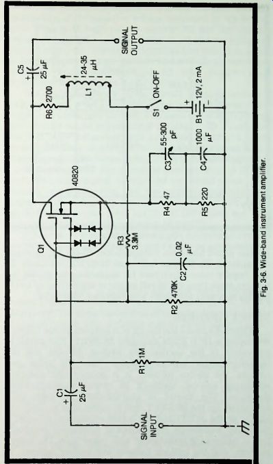
Fig 3-6
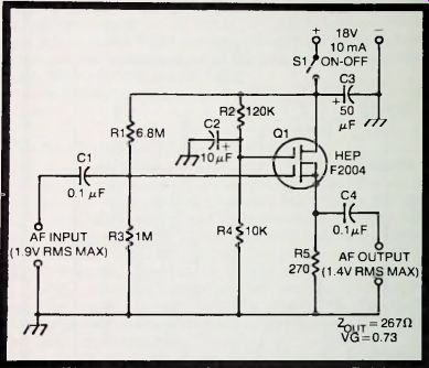
Fig. 3-7. Source follower.
Successful high-frequency performance of the circuit demands that all wiring be short, rigid, and direct, and that leads be dressed for optimum performance and minimum cross coupling.
In this circuit, the MOSFET receives its negative gate-1 bias from the voltage drop resulting from the flow of drain current through source resistors R4 and R5 in series, and its positive gate-2 bias from voltage divider R2-R3, RF-bypassed by capacitor C2. With an individual MOSFET, resistance R3 may require some adjustment for maximum gain at 1000 Hz.
Current drain from the 12-volt supply is approximately 2 mA, but this may vary somewhat with individual MOSFETs.
SOURCE FOLLOWER
Figure 3-7 shows the circuit of a compact source follower employing a HEP F2004 dual-gate MOSFET. This circuit is equivalent to the vacuum-tube cathode follower and the bipolar-transistor emitter follower. Like the latter two circuits, the source follower is a degenerative amplifier employing current feedback to cancel stage-introduced distortion. The circuit is characterized by high input impedance (in the MOSFET. this is higher than in either the bipolar or the JFET) and low output impedance. As such, it has many well-known applications in electronics, especially that of impedance transformer with power gain. The source follower, like the cathode follower and emitter follower, is noted also for its wide frequency response and low distortion.
Q MULTIPLIER
A Q multiplier is a special oscillator that is connected across a tuned circuit in a receiver to increase the latter's selectivity. The Q multiplier thus effectively increases the Q of the tuned circuit. This oscillator may be added either to an RF stage or IF stage. Figure 3-8 shows the circuit of a Q multiplier which can be used in conjunction with a 455 kHz IF stage.
This circuit is basically a Colpitts IF oscillator employing a 3N187 gate-protected MOSFET; it is connected to the IF stage in the receiver through capacitor C2. The Colpitts oscillator employs a single inductor (L1) and split tuning capacitor (C5 and C6) in series. With the resulting 0.005 u-F capacitance, the inductance of L1 (J. W. Miller No. 21A224RBI or equivalent) can be set. by means of the tuning slug, to 244 uH for oscillation at 455 kHz. The strength of oscillation is governed by the setting of the 25 K wirewound oscillation control potentiometer. R4. At one setting of this control, the In this circuit, the negative DC bias on gate 1 is the combination of the negative voltage developed by the flow of drain current through source resistor R5 and the positive voltage developed by voltage divider R1-R3 (the net voltage at gate 1 is negative). The required positive bias voltage on gate 2 is developed by voltage divider R2-R4. With an individual MOSFET. resistances R1 and R2 may require some adjustment for maximum signal output.
The input resistance of the circuit is approximately 1 megohm, and is largely determined by input resistor R1.
Higher resistance may be used, with some risk of stray pickup.
The effective output impedance of the stage is 267.2 ohms; but this will vary somewhat with individual MOSFETs, since transconductance is a factor in the determination of output impedance, and this varies in MOSFETs of the same type.
Voltage gain of the circuit is approximately 0.73. The maximum input-signal voltage before output-signal peak clipping is 1.9-volts rms, and the corresponding maximum output-signal voltage is 1.4-volts rms. The circuit draws approximately 10 mA from the 18-volt DC source, but this may vary somewhat with individual MOSFETs.
All resistors are 0.25-watt. Electrolytic capacitors C2 and C3 are 25-volt units; capacitors C1 and C4 may be any convenient low-voltage units...
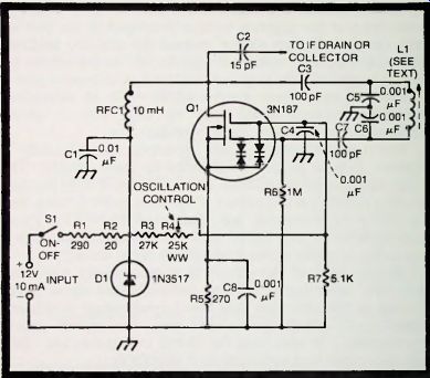
Fig. 3-8 Q multiplier(455 kHz IF).
...signal in the receiver is caused to peak sharply; at another setting of R4. a slot is created, and the signal is eliminated.
In this circuit, gate 1 of the MOSFET receives its negative bias as the voltage developed by the flow of drain current through source resistor R5. Gate 2 receives its positive bias from voltage divider R3-R4-R7. The DC voltage presented to the circuit is regulated by a 1N3517 zener diode in conjunction with resistors R1 and R2 at the constant value of 9.1 volts. (See section 8 for treatment of zener diodes.) When fully oscillating, the circuit draws approximately 10 mA from the 12-volt DC supply.
RF output from the circuit is coupled to the drain or collector of the IF stage in the receiver through 15 pF capacitor C2. All wiring within the Q multiplier and in the receiver to which it is connected must be as short and direct as possible. If the Q multiplier is an external unit, it must be enclosed in a metal shield box inside which all grounds must be returned to a single point. The Q-multiplier ground must be the same as the receiver ground. For stability, all capacitors in and the Q multiplier must be silvered mica, and all resistors should be 1-watt.
Also usable in this circuit is the 40820 MOSFET.
WIDE-RANGE LC CHECKER
Figure 3-9 shows an inductance-capacitance checker circuit employing a HEP F2005 MOSFET. This circuit allows a variable-frequency audio generator (tuning from 20 Hz to 20 kHz) to be used to measure inductance from 6.3 mH to 6329 H and capacitance from 0.0632 pF to 63,291 pF. Other; capacitance ranges may be obtained by changing the value of inductance L1. and other ranges of inductance may be obtained by changing the value of capacitance C2.
The MOSFET is connected in a source follower circuit which drives a series-resonant circuit containing the unknown capacitance connected in series with a known inductance, LI, or the unknown inductance connected in series with a known capacitance. C2. The generator is tuned for peak deflection of meter Ml, which is part of an AC milliammeter circuit connected in the series-resonant circuit. At that point, the generator frequency is noted, and the unknown component calculated in terms of the known values. Thus.
Cx = 1/(39 5 f2 L* )
Lx = 1/(39.5f2 C2).
The unknown component is connected to terminals X-X. Resonant current flowing through 100-ohm resistor R3 develops a voltage drop across this resistor, and this voltage is rectified by diode D to deflect meter M1. The standard inductor (LI) is a 1 mH. slug-tuned coil (J. W. Miller No. 22A103RBI or equivalent) which may be set exactly to 1 mH with the aid of an inductance bridge. Standard capacitor C2 is a 0.01 pF silvered-mica unit which must be obtained with the highest accuracy possible.
----------------
Capacitance Measurement
To use the instrument for determining capacitance values, follow this procedure:
1-Connect the signal generator to the AF input terminals.
2- Connect the unknown capacitor to terminals X-X.
3- Set switch S1 to C.
4- Close switch S2 and turn on generator.
5- Tune generator throughout its range, watching for a peak deflection of meter Ml.
6- At peak, read frequency from generator dial.
7- Calculate the capacitance: C = 1/(0.0395 f2), where C is a farads and f in hertz. Note that the formula is simplified, since the inductance of L1 is constant.
-----------
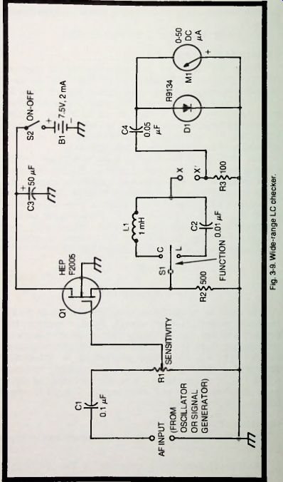
Fig. 3-9
INTERVAL TIMER
Figure 3-10 shows the circuit of a conventional interval timer in which the very high input resistance of the 3N142 MOSFET affords performance comparable to that of the usual vacuum-tube timer. Because of the smallness of the MOSFET, In this circuit, the MOSFET receives its negative gate bias from the voltage drop resulting from the flow of drain current through source resistor R2. The sensitivity control potentiometer, R1, is set for best deflection of meter M1.
Electrolytic capacitor C3 is a 25-volt unit. C2 is silvered mica, and C1 and C4 may be any convenient low-voltage units. For best stability, resistors R2 and R3 should be 1-watt.
The circuit draws approximately 2 mA from the 7.5-volt DC supply, but this current may vary somewhat with individual MOSFETs.
Inductance Measurement
To use the instrument for determining inductance values, follow this procedure:
1- Connect the signal generator to the AF input terminals.
2- Connect the unknown inductor to terminals X-X.
3- Set switch S1 to L.
4- Close switch S2 and turn on generator.
5- Tune generator throughout its range, watching for a peak deflection of meter Ml.
6- At peak, read frequency f from generator dial.
7- Calculate the inductance: L = 1/(3.95 f^2 x10^-7), where L is in henrys and f in hertz. Note that the formula is simplified, since the capacitance of C2 is constant.
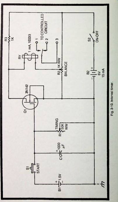
Fig. 3-10
CAPACITANCE RELAY
Capacitance relays are found in a number of electronic systems. They are found also in non-electronic areas, where they serve as object- or people-counters, intrusion alarms, proximity detectors, safety switches, crowd stoppers in exhibitions and displays, and so on. A solid-state capacitance relay is both small and fast-acting.
Figure 3-11 shows the circuit of a capacitance relay employing a 3N128 MOSFET in the sensitive RF oscillator stage and a 2N2716 silicon bipolar transistor in the high-gain DC relay-amplifier stage. In this arrangement, MOSFET Q1 the relay, the 1000 u-F (3V) capacitor, and other components, the entire unit can be very small and compact.
In this arrangement, the single-gate. 3N42 MOSFET serves as a simple DC amplifier driving relay RY in its drain output circuit. When pushbutton switch S1 is depressed momentarily, capacitor C1 is charged from 1.5-volt cell B1. At the same time, relay RY closes. When S1 then is released, capacitor C1 discharges at a rate determined by capacitance C1 and the resistance setting of R1 (the time interval before the relay drops out is closely equal to the time constant of the circuit where t = R1C1 seconds).
The time instant at which the relay drops out may be controlled by proper setting of rheostat R1. With the 50.000-ohm rheostat and 1000 u-F capacitor shown, the maximum time interval is 50 seconds. Other maximum values may be obtained by appropriate selection of C1 and R1 values in accordance with the time-constant formula.
The relay is a 1 mA. 100-ohm device (Sigma 5F-1000 or equivalent) operated in a four-arm bridge in the drain circuit of the MOSFET. The bridge--consisting of resistor R3, the two "halves" of balance control potentiometer R2, and the internal drain-to-source resistance of the MOSFET--allows the static drain current to be balanced out of the relay (by adjustment of potentiometer R2) before the timer is ready to operate.
When the relay is closed, current drawn from the 6-volt DC supply is approximately 15 mA. but this may vary somewhat with individual MOSFETs. Controls R1 and R2 both are wirewound. Resistor R3 is Vk-watt. The 1.5-volt cell, B1, is used only intermittently, to supply charging current to capacitor C1. and should enjoy long life, especially if a size-D cell is used.
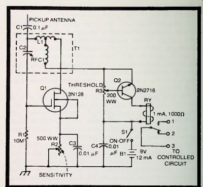
Fig. 3-11. Capacitance relay.
operates as an oscillator in conjunction with inductor L1, trimmer capacitor C2. and radio-frequency choke RFC1 (the inductor, trimmer, and RF choke are self-contained in a commercial capacitance relay coil. J. W. Miller No. 695 or equivalent). The MOSFET stage oscillates lightly; and when a hand or other part of the human body comes near the pickup antenna (a short piece of wire with or without a metal plate on its end), the drain current of the MOSFET undergoes a slight change. This change is coupled to the input circuit of the 2N2716 DC amplifier which, in turn, closes the relay. When the hand is withdrawn, the events reverse and the relay opens.
To set up the device initially, protect the pickup antenna from any nearby bodies, including the operator's. Then, work back and forth between adjustments of threshold control R3 and sensitivity control R2 until the relay just opens. Next, bring one of your hands close to the antenna and alternately adjust trimmer C2 and rheostat R2 with the other hand until the relay just closes. Withdrawing your hand from the vicinity of the antenna should then cause the relay to open. When the circuit is correctly adjusted, bringing the hand to a desired distance from the antenna should close the relay, and moving the hand away should reopen it. The circuit must not be so sensitively adjusted that it self-operates.
For reliable operation, the device should be built solidly and should be completely enclosed in a shield box, except for the pickup antenna. The assembly should be grounded to earth. The antenna must be steady. Capacitor C3 should be a mica or good-grade ceramic unit, but capacitors C1 and C4 can be any convenient low-voltage units. Controls R2 and R3 both are wirewound.
The relay is a 1 mA. 1000-ohm device (Sigma 5F-1000 or equivalent). When the relay is closed, current drain from the 9-volt DC supply. B1. is approximately 12 mA, but this may vary somewhat with individual 3N128s and 2N2716s. Use output terminals 1 and 3 when relay closure must close an external circuit; use output terminals 2 and 3 when relay closure must open an external circuit.
TOUCH-PLATE RELAY
The high input resistance, high transconductance, and low input capacitance of the MOSFET suit this device for use as a DC amplifier in touch-plate relay circuits. Figure 3-12 shows a simple touch-plate circuit that responds to a light touch of a finger. Such relays have become common for operating all sorts of electrical gear, from sophisticated electronic circuits to elevators. A 3N152 low-noise MOSFET is employed in the circuit shown here. The gate almost floats, being 22 megohms above ground through resistor R1. and is connected to a small, metal, pickup disc. The gate thus is highly susceptible to pickup, so that merely touching it with a finger tip couples in enough random energy from stray fields to drive the MOSFET.
The MOSFET serves as a simple DC amplifier with a milliampere-type DC relay in its drain circuit. The relay is connected in a four-arm bridge circuit-consisting of resistor R3. the two "halves" of potentiometer R2, and the internal drain-to-source resistance of the MOSFET-which allows the static drain current of the 3N152 to be balanced out of the relay (by adjustment of R2). The relay is a 1 mA, 1000-ohm device (Sigma 5F-1000 or equivalent).
With the pickup disc protected from any nearby bodies, initially set balance control potentiometer R2 to the point at which the relay opens. The circuit will then remain in this balanced, or "zero," condition indefinitely, unless the setting of R2 subsequently is disturbed. When the pickup disc is touched, the resulting change in drain current will change the internal resistance of the MOSFET. unbalancing the bridge and causing the relay to close.
Use output terminals 1 and 3 for operations in which the external controlled circuit must be closed by the relay closure; use 2 and 3 for operations in which the external controlled circuit must be opened. When the relay is closed, current drain from the 12-volt DC supply is approximately 22 mA, but this may vary somewhat with individual MOSFETs.
ELECTROSCOPE
An instrument for detecting the presence of electric charges is indispensable in many situations, in and out of the electronic field. For instance, it may be used to "smell out" dangerous charges of fields, or to detect the presence of high voltage without making connections to a conductor.
The old fashioned gold-leaf electroscope has a long record of usefulness as such a detector, but this device must be held upright at all times. An electronic electroscope (see circuit in Fig. 3-13) is not so restricted; it may be held in any position and, like the gold-leaf unit, it needs no connection to the source of high voltage.
This arrangement is similar to an electronic DC voltmeter. The gate of the 3N128 MOSFET is 22 megohms above ground and therefore very susceptible to nearby electric charges which are picked up by a polished brass ball on the end of a short rod attached to the gate. The picked-up energy is amplified by the MOSFET, and the latter drives miniature microammeter Ml.
As in an electronic voltmeter circuit, the indicating meter is connected in a four-arm bridge circuit in the output of the MOSFET. The arms of this bridge consist of rheostat R4. the internal drain-to-source resistance of the MOSFET, and resistors R2 and R3. With the pickup ball clear of any electric fields and pointed away from the operator's body, potentiometer R4 is set to zero the meter. The device then will respond by an upward deflection of the meter whenever the ball is poked into a field. A substantial deflection is obtained, for example, when the ball is close to the high-voltage wiring in a TV receiver, or when it is confronted with a hair comb that has just been used.
Current drain from the 9-volt battery. B1, is approximately 12 mA. but this may vary somewhat with individual MOSFETs. All fixed resistors are Vz-watt.
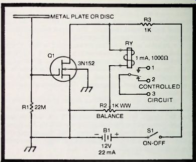
Fig. 3-12. Touch-plate relay.
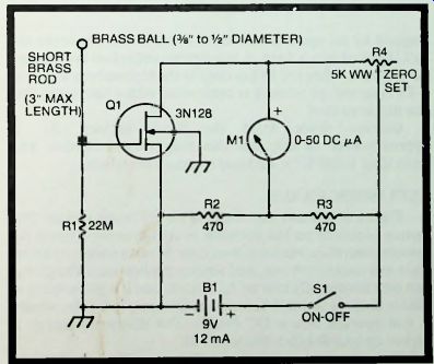
Fig. 3-13. Electroscope (charge detector).
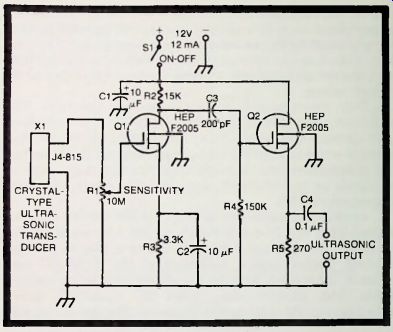
Fig. 3-14. Ultrasonic pickup.
ULTRASONIC PICKUP
Figure 3-14 shows the circuit of an ultrasonic pickup. This device functions as the receptor in an ultrasonic system for remote control, intrusion alarm, code or voice communication, tests and measurements, and similar applications. The pickup can operate directly into an AC circuit; and if a germanium or silicon diode is shunted across the ultrasonic output terminals, it can operate into a DC circuit. The ultrasonic energy is picked up by a 40 kHz transducer. XI.
The circuit consists of a voltage amplifier employing a HEP F2005 single-gate MOSFET (QI) in a common-source arrangement, and a source follower also employing a HEP F2005 MOSFET (Q2). The voltage gain of the input stage is approximately 30. and that of the output stage approximately 0.7: the gain of the entire pickup circuit thus is approximately 21. The maximum transducer signal, with sensitivity control potentiometer R1 set for maximum sensitivity, is approximately 50 mV rms before peak clipping in the output signal. The corresponding maximum output-signal voltage is approximately 1.05 V rms. In construction of this device, solid mounting and rigid wiring should be employed, to prevent vibration at very high frequencies.
All fixed resistors in this circuit are 1/2-watt. Electrolytic capacitors C1 and C2 are 25-volt units; capacitors C3 and C4 can be any convenient low-voltage units. The circuit draws approximately 12 mA from the 12-volt DC supply, but this may vary somewhat with individual MOSFETs.