The integrated circuit (IC) consists of a tiny silicon chip which houses a series of components-such as transistors, diodes, resistors, and capacitors-and the interconnecting conductive paths which serve as wiring. These components and paths are formed by a combination of diffusion, photo printing, and etching. Thus, the chip can contain an entire complicated circuit, such as a multistage amplifier, and the IC will be no larger than a discrete transistor.
The type CA3010 integrated circuit, for example, is a direct-coupled operational amplifier containing 10 transistors, 2 diodes, and 18 resistors; it has 12 leads for external connections and is housed in a TO-5 transistor package.
Depending upon type, the IC is provided with pigtail leads or with terminal tabs, allowing the IC to be inserted into a socket or to be wired directly into an external circuit.
The IC, being a complete, miniaturized circuit package, saves much time and labor for the designer and builder of equipment; an entire pre-wired stage (or full circuit) can be plugged in or removed from a piece of equipment with the ease of handling a transistor or tube. While a large number of ICs contain complicated circuits, some contain only separate components (for example, 2 diodes or 4 transistors) which, being fabricated close together in the same substrate, are excellently matched. Integrated circuits are available in a very large number of types in both linear and digital categories.
Before working with Ics, read the hints and precautions in Section 1, especially items 3,4, 6. 8, 10, and 14.
IC THEORY
Figure 4-1 (A) shows the structure of a possible integrated circuit; Fig. 4-1 (B) shows the corresponding internal circuit.
While this arrangement is not necessarily one that can be found in a manufactured unit, it is true to the nature of the IC and is simple enough for illustrative purposes.
In Fig. 4-1 (A), N- and P-regions are diffused into the substrate (silicon chip) to form the diode (D1), transistor (Q1), resistor (RD. and capacitor (C1) of the circuit. Next, a silicon dioxide dielectric film is grown on the face of the chip.
Then this dielectric is etched away at those places, such as points 4 and 10. where connections must be made to the N- and P-regions. Next, a metal film is deposited on top of the dielectric to extend through the etched windows to make contact with the regions and to provide the "wiring" between the components. The matching numbers in Fig. 4-1 (A) and 4-1 (B) allow these contacts and interconnections to be identified by the reader.
In this example, the various components are formed in a P-type chip; and since each component has an "outside" N-layer, the resulting PN junction offers very high resistance, being reverse biased, and thus prevents the components from being short-circuited together through the substrate. The resistor consists only of a P-region. connections being made to the latter at points 7 and 8. One "plate" of the capacitor is the N-region. to which a connection is made at point 10, and the other plate is the portion "X" of the metal film. This general construction is characteristic of all ICs, although the geometry of a specific manufactured unit may differ considerably from the structure in Fig. 4-1 (A).
The various functional types of ICs are too numerous to list here. However, some familiar examples are DC, AF, IF, RF, video, differential, and operational amplifiers; balanced modulators; product detectors; mixers; and amplifier/ discriminators in the linear category; and flip-flops; gates; latches; inverters; Schmitt triggers; and scalars in the digital category.
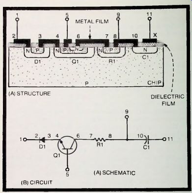
Fig. 4-1. Details of integrated circuit.
Figure 4-2 shows circuit symbols for various types of IC. In circuit diagrams in which these symbols appear, up to 14 numbered leads (not shown in Fig. 4-2) are drawn to these symbols. The numbering corresponds to the lead or terminal numbering of the particular IC package. Figures 4-2 (A) and (B) are linear-type ICs; Figs. 4-2(C), (D), (E), (F), and (G) are digital type; Fig. 4-2(H) may be either linear or digital and represents any other undesignated type such as a type voltage regulator or interval timer.
Figure 4-3( A) shows the internal circuit of a type CA3002 IF amplifier IC, and Fig. 4-3(B) shows the corresponding circuit symbol with leads numbered according to the terminal numbering of the actual IC package.
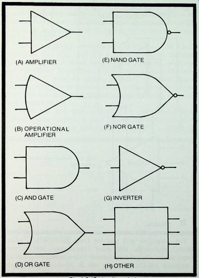
Fig. 4-2. IC circuit symbols.
COMPLETE AUDIO AMPLIFIER
One of the attractions of the IC to experimenters and some audiophiles is the ability of some ICs to supply a complete audio amplifier in a small transistor-type case. An amplifier of this type is shown in Fig. 4-4. Here, the CA3020 integrated circuit contains three intermediate stages and a push-pull, class-B output stage. The only "outboard" components required are four capacitors, two fixed resistors, one potentiometer, and one output transformer. The circuit operates from a single battery.
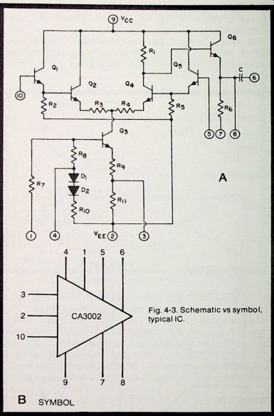
Fig. 4-3
The amplifier will operate from microphones, phono pickups, photocells, and other transducers, and delivers 14-watt output. Output transformer T1 is a miniature unit, such as Argonne AR-174, having a 100- or 125-ohm center-tapped primary winding and 3.2-ohm secondary, to match the 3.2-ohm speaker to the IC.
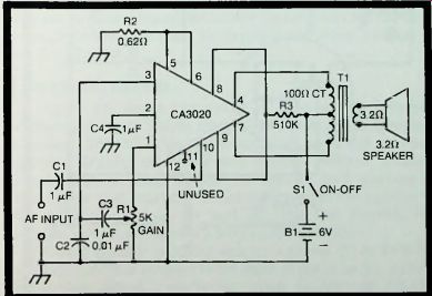
Fig. 4-4. Complete audio amplifier.
The class-B output stage uses most of the DC input power; thus, the idling current drain from the 6-volt battery is approximately 4 mA. and the maximum-signal current is 77 mA. At a battery voltage of 9 volts, the current drains are somewhat higher, and the power output is approximately 0.3 watt. With either 6- or 9-volts input, however, the IC must be supplied with a suitable heat sink.
The amplifier exhibits good gain. An input of 50 mV rms results in full Vi-watt output with low distortion, when gain control R is set for maximum gain. This operation allows the amplifier to function as the complete AF channel of a receiver, monitor, or test instrument. It also serves as its own integral audio amplifier.
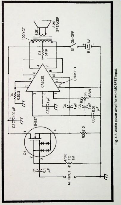
Fig. 4-5
For best stability, resistors R2 and R3 should be 1 watt.
Capacitors C1, C3. and C4 can be miniature tantalum electrolytics. if maximum compactness is desired; otherwise any convenient low-voltage non-electrolytics may be used.
Capacitor C2 may be paper, ceramic, or mica. Size-D flashlight cells give reasonably good service for short-interval operation, but miniature transistor-type batteries are short lived in this circuit.
Other ICs are also available for complete-amplifier operation. One example is type LM380. This type delivers 2^2 watts (total harmonic distortion = 0.2%) with a 22-volt DC supply, and operates directly into an 8-ohm speaker without output transformer.
AUDIO POWER AMPLIFIER WITH MOSFET INPUT
The versatility of the complete audio amplifier described in the preceding section can be widened by providing it with a high-impedance input stage. Figure 4-5 shows how a 3N87 MOSFET is employed as a simple source follower to provide this high impedance. (See Section 3 for MOSFET theory and application.) The voltage gain of the input stage is approximately 0.51, and this requires that the input signal amplitude be 98 mV rms for a full Vi-watt output into the speaker. For this circuit, the zero-signal current from the 6-volt battery is 14 mA, and the maximum-signal current is 87 mA. These are approximate figures and will vary somewhat with individual ICs and MOSFETs.
Five outboard components are required for the MOSFET: Capacitor C2 is a 25-volt electrolytic unit, while C1 may be any convenient low-voltage unit. Resistors R1 and R2 are 1/4-watt.
All outboard components in the IC portion of the circuit correspond to those in the same positions in the basic IC circuit. Fig. 4-4.
For ease of handling and installation, a gate-protected MOSFET has been chosen; however, a conventional MOSFET also can be used if the experimenter is experienced in handling the unprotected type (see. for example, the source follower in Fig. 3-7, Section 3).
2 1/2-WATT INTERCOM
Figure 4-6 shows the circuit of a miniature intercom employing a type LM380 integrated circuit as the complete amplifier. This IC delivers 2 1/2-watts output at full gain and operates directly into an 8-ohm speaker, without coupling transformer. A small speaker is used at both stations as microphone and reproducer, depending upon the position of the talk-listen switch. S1 and S3. The two stations are interconnected by means of a 3-wire. shielded cable.
When a speaker is acting as a microphone ( S1 or S3 in the talk position), it is coupled to the input of the IC by T1, a small 4000:8 ohm output transformer (such as Argonne AR-134) connected backward. The other speaker then is automatically connected to the output of the IC and serves as a reproducer. The 2 1/2-watt output will be adequate in all except very noisy places.
Construction of the intercom should be entirely straight-forward. Take special precautions to keep the input and output circuits of the IC as isolated as well as practicable, to prevent unwanted electrical feedback, and to provide the IC with a heat sink. Aside from the input coupling transformer, the only outboard components are the 1-megohm rheostat (R1)
and 500 mF output capacitor (C1).
Current drain from the 22.5-volt DC source, B1, is approximately 25 mA zero-signal, and 220 mA maximum signal. These currents may vary somewhat with individual ICs.
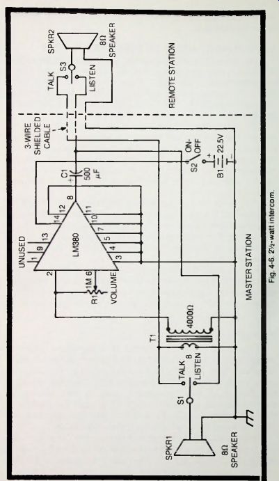
Fig. 4-6
VERY LOW-RESISTANCEDC MILLIAMMETER
Low resistance is desired in a current meter, in order to minimize the voltage drop introduced by the meter into a% circuit where it is inserted. The more closely the internal resistance of the meter approaches zero, the less the instrument upsets the circuit. Even though the resistance of many current meters is low. it still is too high for some applications unless it is painstakingly taken into account in all measurements and calculations. For example, the common resistance of the useful 0-1 DC milliammeter is 55 ohms, corresponding to a voltage drop of 55 mV.
Figure 4-7 shows the circuit of an electronic DC milliammeter giving a full-scale deflection of 1 mA and having a resistance of only 2.7 ohms. In this circuit, the type p.A776 integrated circuit functions as a DC voltage amplifier with a voltage gain of approximately 40, and boosts the 2.7 mV developed by the 1 mA input current across resistor R1 to the 100 mV required to deflect the 0-50 DC microammeter (M1) to full scale. If this microammeter-whose internal resistance is 2000 ohms-were simply shunted to convert it into a 0-1 milliammeter, a shunt resistance of 105 ohms would be required, and the resulting instrument resistance would be 99.8 ohms, approximately 37 times the input resistance of the electronic circuit.
In this circuit, resistors R1, R2, and R4 must be selected to have resistance as close as practicable to the specified values.
If precision instrument resistors are available to the builder.
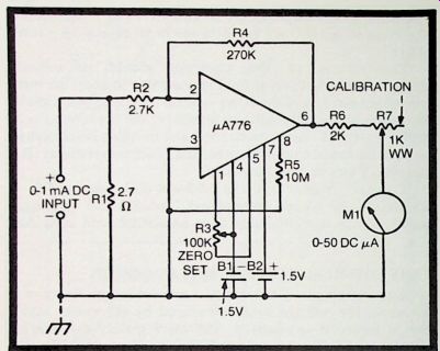
Fig. 4-7. Very low-resistance DC milliammeter.
R1 can be 2 ohms. R2 2 K. and R4 200 K; the input resistance then will be 2 ohms. Meter Ml is initially set to zero by adjustment of potentiometer R3 which adjusts the offset of the IC. Rheostat R7 allows the meter to be set for exact full-scale deflection when an accurately known 1 mA current is applied to the DC input terminals. For best stability, resistors R1, R2, and R4 should be 1-watt each. Resistors R5 and R6 may be 1/2-watt. Rheostat R7 must be wirewound.
Initial adjustment of the instrument is simple:
1- With the DC input terminals open, set rheostat R7 to its zero-resistance position and set potentiometer R3 to zero the microammeter.
2- Apply an accurately known 1 mA direct current to the DC input terminals.
3- Adjust rheostat R7 for exact full-scale deflection of the meter.
4- The instrument response is linear, and may be checked by applying successively lower currents (such as 1/2 mA, 1/4 mA, etc.) to the DC input terminals.
A special 0-1 mA card may be drawn for the meter, or the 0-50 u-A card may be retained and the readings in mA interpreted from the u-A deflections.
An added advantage of this circuit is its low power demand. Size-D flashlight cells at B1 and B2 will give shelf life, so no on-off switch is required.
ELECTRONIC DC MILLIVOLTMETER
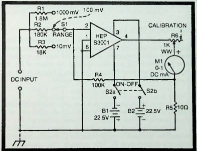
Fig. 4-8. Electronic DC millivoltmeter.
Figure 4-8 shows the circuit of an electronic DC millivoltmeter covering 0-1000 mV in three ranges: 0-10 mV, 0-100 mV. and 0-1000 mV. Readings are displayed on the scale of a 0-1 DC milliammeter. In this circuit, a type HEP S3001 integrated circuit functions as a DC voltage amplifier to boost the input-signal voltage to the 55 mV required for full-scale deflection of the milliammeter.
The circuit is relatively uncomplicated. The input portion contains only the three multiplier-type range resistors (R1, R2, R3) and the range selector switch (S1). Negative feedback through the 100K resistor, R4 sets the gain of the amplifier and also linearizes response of the milliammeter. A dual DC supply (22.5-volt batteries B1 and B2) is required; the current drain from each battery is approximately 5 mA, but this may vary with individual ICs. No zero-set potentiometer is needed.
For best stability, all fixed resistors in the circuit should be 1-watt. Resistors R1, R2. and R3 must be selected as close as practicable to specified values (they may depart from these values, so long as all three vary by the same ratio). Rheostat R6 must be wirewound. All wiring should be kept as short and direct as possible. Unused terminals of the IC may be left floating.
To calibrate the instrument initially:
1- Set switch S1 to its 1000 mV position.
2- Set calibration rheostat R6 to its zero-resistance position. Close switch S2.
3- Apply an accurately known 1-volt DC to the DC input terminals, observing correct polarity.
4- Adjust rheostat R6 for exact full-scale deflection of milliammeter M1.
5- Operation of the circuit is linear, and this may be checked by applying successively lower voltages (with S1 still set to the 1000 mV range), such as 1/2-volt, 14- volt. etc., while observing deflection of the meter.
6- If resistors R1, R2, and R3 are accurate, this one calibration will serve also for the 100 mV and 10 mV ranges which will then be automatically in calibration.
----------
LOW-PASS ACTIVE FILTER
Figure 4-9 shows the circuit of a low-pass active filter employing a type 741 operational-amplifier IC. This circuit provides a cutoff frequency of 500 Hz, but may be adapted to other frequencies by suitably changing the values of R1, R2, C1, and C2. (For other frequencies, keep R1 equal to R2, and C1 equal to C2. The cutoff frequency fc equals:
fc = 10^6/(2 pi RC) where fc is in Hz. R in ohms, and C in u-F.)
Beyond the cutoff frequency, the response of the circuit falls off at the rate of 12 dB per octave. Overall voltage gain is approximately 1.59.
Negative feedback is provided by voltage divider R3-R4, and positive feedback through capacitor C1 which is part of the frequency-determining FC filter network. This application of feedback, provided by the amplifier, sharpens the response of the filter beyond that of the simple RC circuit (R1-R2-C1-C2).
A dual DC supply is required, represented here by 12-volt batteries B1 and B2. The drain from each battery is approximately 3 mA, but this can be expected to vary somewhat with individual ICs.
All wiring must be kept as short and well separated as practicable, to prevent signal transfer around the IC; in other respects, however, construction of this filter offers no special problems. Resistances R1 and R2 must be accurate, as must also capacitances C1 and C2. The 0.032 pF capacitance can be obtained by connecting one 0.03 and one 0.002 uF capacitor in parallel. These capacitors must be of good quality. All resistors should be 1-watt. DC coupling is shown in Fig. 4-9, but AC coupling may be obtained by connecting one 10 pF capacitor in series with the high AF input lead, and another in series with the high AF output lead.
HIGH-PASS ACTIVE FILTER
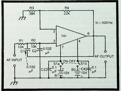
Fig. 4-9. Low-pass active filter.
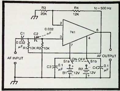
Fig. 4-10. High-pass active filter.
Figure 4-10 shows the circuit of a high-pass active filter employing a type 741 operational-amplifier IC. This circuit, like the low-pass filter described in the preceding section, provides a cutoff frequency of 500 Hz. but may be adapted to other frequencies by suitably changing the values of R1, R2, C1, and C2. For other frequencies, keep R1 equal to R2, and C1 equal to C2. The cutoff frequency fc equals:
fc = 10^6/(2 pi RC) where fc is in Hz. R in ohms, and C in u-F.
Below this cutoff frequency, the response of the circuit rises at the rate of 12 dB per octave. Overall voltage gain is approximately 1.59.
Negative feedback is provided by voltage divider R3-R4, and positive feedback through resistor R1 which is part of the frequency-determining RC filter network. This application of feedback, provided by the amplifier, sharpens the response of the filter beyond that or the simple RC circuit (R1-R2-C1-C2).
A dual DC supply is required, represented here by batteries B1 and B2. The drain from each battery is approximately 3 mA, but this can be expected to vary somewhat with individual ICs.
All wiring must be kept as short and well separated as practicable, to prevent signal transfer around the IC; in other respects, however, construction of this filter offers no special problems. Resistances R1 and R2 must be accurate, as must also capacitances C1 and C2. The 0.032 uF capacitance can be obtained by connecting one 0.03 and one 0.002 uF capacitor in parallel. These capacitors must be of good quality. All resistors should be 1-watt. The input is AC coupled by the first filter capacitor, C1, but the output is DC coupled. If desired, the output can be AC coupled by inserting a 10 uF capacitor in the high AF output lead.
COMBINATION HIGH-PASS, LOW-PASS ACTIVE FILTER
The active filter circuit shown in Fig. 4-11 is. in effect, a combination of a low-pass filter and high-pass filter. A single pair of resistors (R1-R2) and a single pair of capacitors (C1-C2) are arranged into a low-pass RC filter circuit when the 4-pole, double-throw changeover switch (S1 a-d ) is in its LP - position, and are arranged into a high-pass RC filter circuit when the switch is in its HP position.
With the R1-R2 and C1-C2 values given in Fig. 4-11, the cutoff frequency is 500 Hz for both the low-pass and high-pass functions. The cutoff frequency may be changed to some other * desired value-and will be the same for low-pass and high-pass-by suitably changing the values of R1, R2, C1, and C2. For other frequencies, keep R1 equal to R2, and C1 equal to C2. The cutoff frequency fc equals:
fc = 10^6/(2 pi RC) where fc is in Hz. R in ohms, and C in uF.
Above this frequency, in the low-pass function, the response of the circuit falls off at the rate of 12 dB per octave; below this frequency, in the high-pass function, the response rises at the rate of 12 dB per octave.
The general characteristics and construction of this filter are the same as those separately described for the low-pass filter and for the high-pass filter. See earlier sections of this section for this information. The combination filter has DC-coupled output, but the input is inherently DC coupled on low-pass and AC coupled on high-pass. If AC coupling is desired for both high-pass and low-pass and for both input and output, insert one 10 u-F capacitor into the high AF input lead, and another 10 uF into the high AF output lead.
BANDPASS (PEAK) ACTIVE FILTER
Figure 442(A) shows the circuit of a bandpass active filter of the sharp-peak type employing a type 741 operational and amplifier IC. A parallel-T RC network (R3-R4-R5-C2-C3-C4) in the negative-feedback loop determines the peak frequency of this filter. This is a null network, but it makes a pass amplifier out of the circuit, as it cancels gain of the amplifier on all frequencies except the null frequency. Positive feedback is adjustable by means of rheostat R7, and serves to sharpen the response of the circuit, thus effectively increasing the Q of the parallel-T network.
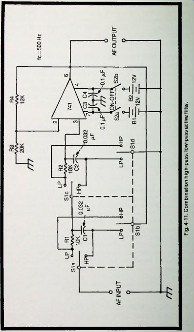
Fig. 4-11
Figure 4-12(B) shows the response of the circuit: The solid curve depicts minimum selectivity (low Q) when positive feedback is minimum (R7 set to maximum resistance), whereas the dotted curve shows maximum selectivity (high Q) when positive feedback is maximum (R7 set to low or zero resistance). Voltage gain of the circuit at the peak of the response is approximately 100.
The resistance and capacitance values in the parallel-T network have been chosen for a filter peak of 1000 Hz. The peak frequency may be changed to some other desired value, however, by suitably changing the values of C2, C3, C4, R3, R4, and R5.
For C2 = C3 other frequencies, keep R3 = R5 = R4,
= ½ C4. The peak frequency f equals:
f = 10^6/(2 pi R3 C2) where f is in Hz. R3 in ohms, and C2 in u-F.
A dual DC supply is required, represented here by 15-volt batteries B1 and B2. The drain from each battery is approximately 4 mA, but this can be expected to vary somewhat with individual ICs.
All wiring must be kept as short and well separated as possible, to prevent signal transmission around the IC; in other respects, however, construction of the filter offers no special problems. Resistances R3, R4, and R5 must be accurate, as must capacitances C2, C3, and C4. The off-standard values for R3 and R5 can be obtained by connecting one 3000- and one 180-ohm resistor in series, and for R4 by connecting one 1500- and one 91-ohm resistor in series.
Capacitors C2, C3, and C4 must be of excellent quality.
It is interesting to note that the filter becomes a sine-wave oscillator when the positive feedback is advanced sufficiently (that is. when selectivity control R7 is set for excessive regeneration).
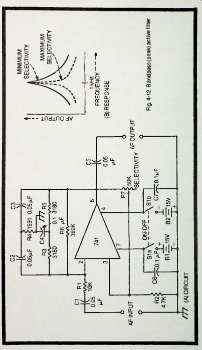
Fig. 4-12
ACTIVE BANDSTOP (NOTCH) FILTER
Figure 4-13(A) shows the circuit of a bandstop active filter of the sharp-notch type, employing a type 741 operations-amplifier IC. A parallel-T RC network (R1-R2-R3-C1-C2-C3) in the input circuit determines the notch frequency of this filter. This is a null network. Positive feedback is introduced at the common point of this network (junction of C3 and R3) to sharpen the response of the parallel-T. Figure 4-13(B) shows typical response.
The resistance and capacitance values in the parallel-T network are stock, and the resulting notch frequency is 1061 Hz. For exactly 1000 Hz. R1 = R2 = 15,915 ohms, R3 = 7957 ohms; and the capacitances remain the same as shown in the circuit. The notch frequency may be changed to any other desired value, by suitably changing the resistance or capacitance values.
For other frequencies, keep C1 = C2 = ^C3, and R1 = R2 = 2R3.
The notch frequency f equals:
f = 10^6 /(2 pi R1 C1 )
... where f is in Hz. R1 in ohms, and C1 in u-F. Voltage gain of the circuit is 1.
A dual DC supply is required, represented here by 15-volt batteries B1 and B2. The drain from each battery is approximately 4 mA, but this can be expected to vary somewhat with individual ICs.
All wiring must be kept as short and well separated as practicable, to prevent signal transmission around the IC; in other respects, however, construction of the filter offers no special problems. Resistances R1, R2, and R3, and capacitances C1, C2, and C3 must be accurate. Furthermore, the capacitors must be of excellent quality.
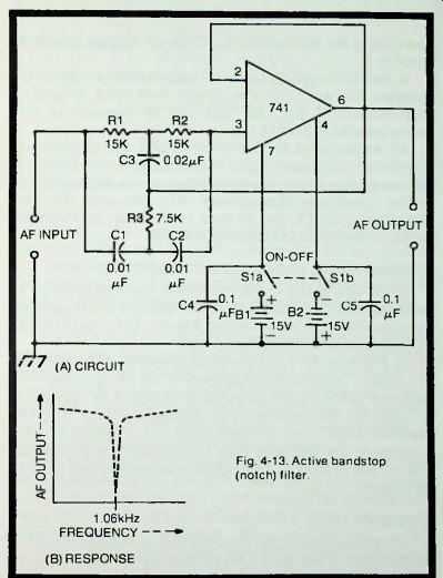
Fig. 4-13. Active bandstop (notch) filter.
CONVENTIONAL BANDPASS ACTIVE FILTER
Users who desire a wider passband than that provided by the notch filter described earlier can cascade a high-pass and a low-pass filter, as shown in Fig. 4-14( A). The response of this arrangement is shown in Fig. 4-14(B).
In Fig. 4-14(B), fC1 is the cutoff frequency of the high-pass unit, and fC2 is the cutoff frequency of the low-pass unit. The high-pass and low-pass units may be designed for the desired fC1 and fc2 frequencies. The passband of the complete bandpass filter then is equal to fC2 - fC1. Below fC1, the response of the bandpass filter rises at the rate of 12 dB per octave; and beyond fC2, the response falls at the rate of 12 dB per octave.
SIGNAL TRACER
An untuned signal tracer remains an invaluable electronic troubleshooting aid. Such a device should provide a reasonable amount of signal sensitivity and visual, as well as aural ...
--------
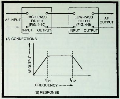
Fig. 4-14. Conventional bandpass active filter.
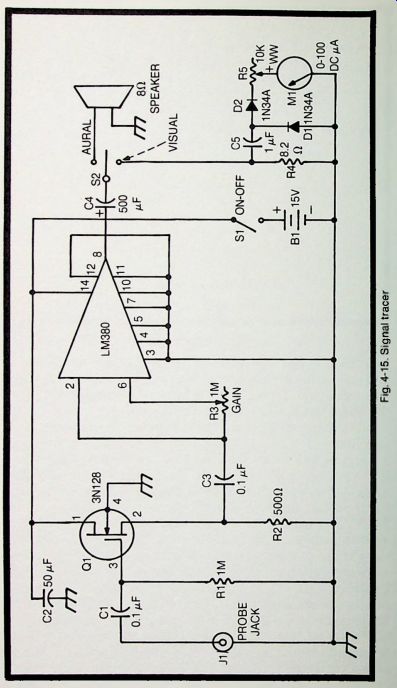
Fig. 4-15
...indications. The conventional signal tracer embodies a high-gain audio amplifier with a power output stage, provides high input impedance, and works from a straight test probe (for audio testing) or a demodulator probe (for modulated-RF testing). Battery operation gives complete isolation from the power line.
Figure 4-15 shows the circuit of an efficient signal tracer that can be built to small dimensions. A type LM380 integrated circuit supplies the high-gain audio amplifier with power-output stage. A source follower, employing a 3N128 MOSFET, connected ahead of the IC provides the very high input impedance. The shielded jack, JI, receives either the straight test probe or the demodulator probe.
When switch S2 is in its aural position, the amplifier drives the 8-ohm speaker; no output transformer is needed. When S2 is in its visual position, the 8.2-ohm resistor, R4, substitutes for the speaker as the amplifier load, and a rectifier-type meter (C5-D1-D2-R5-M1) indicates the output-signal voltage developed across this resistor. Rheostat R5 may be set initially to confine the deflection to full scale when gain control R3 is set for maximum gain (highest tracer sensitivity); R5 then needs no subsequent adjustment, except for periodic realignment to correct aging effects.
Since the IC contains a class-B output stage, the current drawn from the 15-volt DC source (battery B1), varies with the input signal: the zero-signal level is 10 mA, and the maximum-signal level 150 mA.
The simplicity of the circuit insures troublefree construction. Except for the care needed in handling the MOSFET (see precautions in Section 1), no special problems are introduced. Fixed resistors R1 and R2 are 1/2-watt; R4 is 5 watts. Electrolytic capacitors C2 and C4 are 25-volt units; capacitors C1, C3, and C5 may be any convenient low-voltage units, except C5 should not be electrolytic.
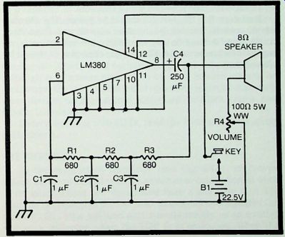
Fig. 4-16. Group code-practice oscillator.
GROUP CODE-PRACTICE OSCILLATOR
The resistance-capacitance AF oscillator shown in Fig. 4-16 delivers enough audio output-approximately 2-watts-to an 8-ohm speaker to serve a group of listeners. The type LM380 integrated circuit operates as a phase-shift oscillator with a phase-lag-type frequency-determining network R2-R3-C1-C2-C3) inserted into its positive-feedback loop.
With the stock resistance and capacitance values in the network, the frequency is 406 Hz. For exactly 400 Hz, with the 1 mF capacitors shown, the resistors would each need to be 688.7 ohms. The frequency of approximately 400 Hz was chosen for its easy "readability." However, the frequency of the oscillator can be changed to any other desired value by suitably changing the resistance or capacitance values in the phase-shift network. For any frequency, keep R1 = R2 = R3, and C1 = C2 = C3, the oscillation frequency f equals:
f = 10*/(3.63 f C)
... and ...
C = 10^6 / (3.63 f R).
The R and C values thus obtained will always produce the required total phase shift of 180 degrees. Resistors R1, R2, and R3 must be accurate, as must also capacitors C1, C2, and C3.
When the key is down, the circuit draws approximately 220 mA from the 22.5-volt DC supply, represented here by battery B1. The IC should be provided with a heat sink.
Resistors R1, R2, and R3 should be 1-watt. The 100-ohm volume control rheostat, R4, must be a 5-watt unit. Capacitors C1, C2, and C3 may be any convenient low-voltage units, so long as they are accurate. Electrolytic capacitor C4 should be a 25-voit unit.