|
|
Low-power FM transmitters have been a popular hobby item in recent years. They are usually free-running oscillators that are frequency modulated with an audio signal and are used in many applications from wireless mikes to "bugs" and for small home FM radio stations covering 100 feet or so. Stereo operation is also possible using a chip, such as the BA1404, and several parts, but the advance of technology has brought out some new problems in using these gadgets. Digitally tuned receivers are commonplace nowadays, including FM broadcast receivers. Digital receivers are always exactly on frequency and make finding a desired station simple. The traditional analog slide rule dial has largely disappeared from the higher-end FM receivers, replaced by LCD or LED readouts. Therefore, the digitally tuned receiver has no need for fine-tuning or automatic frequency control and cannot generally be tuned off channel. This makes it necessary for received signals to be on frequency. Of course, this is no problem because commercial FM stations must be crystal con trolled and held to close tolerances; however, for the user of some simple low-power transmitters, this is a problem because frequency drift is a fact of life for these circuits. It is hard to hold simple LC oscillators to a stability of much better than 0.1 percent, over a reasonable temperature and supply voltage range. At 100 MHz, the middle of the FM broadcast band, this is a drift of 100 kHz.
An analog-tuned FM receiver has no problem receiving the signal as it drifts because the AFC circuit automatically retunes the receiver as needed. A digitally tuned receiver with frequency-synthesized tuning using a phase locked loop (PLL) cannot do this without special circuitry. Commercial FM receivers have no need to do this anyway. Also, the FM band is crowded with many signals in most populated areas, and a free or unoccupied channel is rare at times, so as the low-power FM transmitter drifts, it runs into interference from adjacent channel signals. The solution to this problem is to make the low-power transmitter crystal controlled; however, this is not simple because the 75-kHz frequency deviation needed for FM broadcast work cannot easily be obtained from simple crystal oscillators. It is even difficult to get one-tenth of this (7.5 kHz) and still keep the audio distortion to less than 1 percent. In order to do this, commercial FM transmitters used frequency-multiplier stages and mixers, starting at a low frequency, multiplying up, heterodyning down, and multiplying up again to realize large multiplication factors. In this way, it was possible to get the 75-kHz deviation from a lower-frequency oscillator with a very small deviation.
This traditional method requires a lot of circuitry and is impractical and prohibitively complex and expensive for the hobbyist wishing to experiment with low power, physically small, simple FM transmitters. Fortunately, another approach is made possible by the use of modern digital IC devices. This section describes a simple low-power FM stereo transmitter using PLL techniques, along with a few digital IC devices and analog op-amps, to produce a clean, stable, broadcast-quality FM stereo signal. We call this device the MPX96 low-power FM transmitter.
The MPX96 is a complete PLL-synthesized low-power FM stereo audio link operating in the standard FM broadcast band. It can be operated over the range 76- 108 MHz, therefore supporting North American domestic FM and the 76-88 MHz frequency range used in Asia. Channel spacing is 100 kHz, which ensures coverage of all FM frequencies. Both the FM carrier frequency and the multiplex pilot frequencies are crystal controlled, eliminating the drift that is common with uncontrolled LC oscillators. This permits use of this unit with digital PLL receivers.
Programming consists of setting a 10-position DIP switch with a binary code corresponding to the desired transmitter frequency. This frequency can be any unused FM channel in your area. Once the frequency is set, the MPX96 will stay on that channel because it is phase locked to an internal crystal oscillator. Audio input can be any line-level source of 0.5-1 volt RMS dual-channel audio (stereo or two individual sources). An onboard tone generator (1.2 kHz) is provided for setup purposes. All seven IC devices in the MPX96 are readily available standard ICs. Circuit setup is simple, with only a VOM needed. A single 12- to 15-volt DC negative ground supply is needed to power the MPX96, and because the current drain is 120 mA, a simple battery pack can be used to power it. RF output is about 10 mW into a 50-ohm load (0.7-volt rms). For export use only, this output can be increased to 150 mW with a simple circuit change. The recommended antenna for U.S. operation is a 12-inch whip antenna shunted with a 56-ohm resistor.
Several years ago, the authors published an article describing an MPX transmitter with a free-running oscillator and an MPX generator using several IC devices to generate an MPX baseband signal. The article appeared in the March/April 1988 issues of Radio-Electronics. This circuit worked well, but soon after, the BA1404/BA1405 IC devices appeared, greatly simplifying the task of building an FM stereo transmit ter. The BA1405 was similar to the BA1404 but had no RF section on board the chip. Introduced for the purpose of interfacing with after-market CD players to FM stereo auto radios, these ICs were useful for making a simple stereo transmitter. The BA1404 had poor RF stability, and being a "black box" item, it taught little about MPX circuit operation to the experimenter. It also had the disadvantage of requiring low-supply voltage (less than 3 volts) and required a fragile 38-kHz crystal. Presently, the demand for this device has dropped to the point where it is going to be discontinued by its only manufacturer. We considered using this chip until the manufacturer told us it was to be discontinued past July 15, 1996, after a final "life time buy" production run was made. Although this chip may be available from distributors and surplus houses, in small quantities, for a few more years, it seemed to be unwise to design a transmitter around a chip with no future. Instead, we developed a simple MPX generator using a simplified version of the well-proven 1988 circuit, adding some improvements and eliminating several setup adjustments.
Two IC devices now handle MPX generation, and a crystal-controlled approach replaces the three large coils originally used. The fragile 38-kHz crystal used by the BA1404 for the purpose of pilot and subcarrier has been replaced by a rugged 5-MHz type in our new circuit, and two common CMOS ICs generate the 38-kHz and 19-kHz signals. As an extra bonus, a 1.2-kHz audio signal is developed in one of the ICs at no extra cost. This signal is useful for test purposes. The total cost is low and, unlike the BA1404/BA1405 approach, all of the MPX signal components are available for observation and experimentation. Actually, we were not too impressed with the BA1404 regarding its overall performance: the need for "glue" circuitry to interface this device to the synthesizer was a drawback, and the RF section proved to be totally unsuitable for a really good VCO. The demise of the BA1404/BA1405 is therefore no great loss because much better performance can be had with only a few extra parts and conventional IC devices available from multiple sources.
Typical applications of the MPX96 include, but are not limited to, the following:
1. Home audio systems: Listen to your CD player, tape deck, and the like on a pocket stereo while not in the same room as your audio equipment, or outside the house, in the garage, workshop, deck, and so on.
2. Other applications such as private or inhouse broadcast systems for schools, real estate, health clubs, stores, offices, museums, and so forth.
3. Use as a short-range FM station in remote areas where no other FM reception is possible or no suitable stations can be received.
4. For entertainment of groups in which a second language is spoken. Two languages can be carried, one on each channel, for a bilingual PA system, using small pocket stereo receivers. This is useful for churches, fairs, shows, and the like.
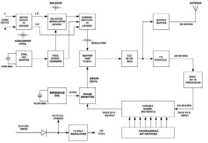 FIG. 1 Block Diagram of the MPX96 Frequency Synthesized FM Stereo Transmitter
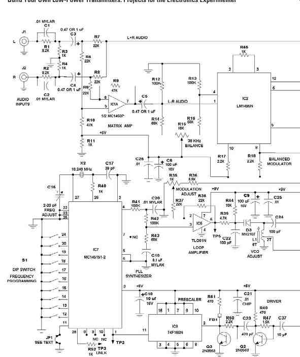
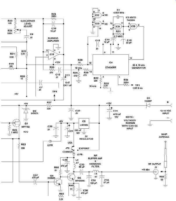
FIG. 2 Schematic of the MPX96 Frequency Synthesized FM Stereo Transmitter
Circuit Operation
The MPX 96 uses eight IC devices and five transistors to implement a complete PLL-synthesized FM stereo transmitter. The transmitter can be broken up into several subsystems, which are the audio and MPX generator, the clock, the PLL, and the output amplifier (see Figures 1 and 2 for reference).
The audio section consists of IC1a and IC1b, a dual op-amp LM1458N, and balanced modulator IC2. Line-level audio inputs of approximately 0.5-1.0 volt RMS (high impedance approximately 10K) connected to both J1 and J2 are fed to an RC preemphasis network R1, C1, R3, and R2, C2, R4, which boost frequency components above 2000 Hz for better signal-to-noise (s/n) ratio. This is done in FM broad casting to improve the s/n ratio. Coupling capacitors C3 and C4 pass these signals to a matrixing circuit consisting of R7 and R8, and a differential amplifier IC1a, and associated components R5, R6, R9, R10, and C5. The L and R audio inputs are combined by R7 and R8 to form a signal that is the sum of the left and right audio channels (L+R), and this is passed to the summing junction of the multiplex amplifier IC1b, where it is combined with two other signals. One of these signals is the audio subcarrier containing the audio information that is the difference of the two inputs L and R, or (L-R). Note that if the two audio inputs L and R are identical, this signal is 0.
IC1a is configured as a differential amplifier with a gain of about 2, and the L audio input is fed to the noninverting input via R5 and R10. A network consisting of R11 and R20 and bypass capacitors C6 and C26 provides a fixed bias of half the nominal 12-volt supply voltage (+6 volt) to bias both IC1a and IC1b inputs. This avoids the need for separate plus and minus supplies. The R input is fed to the inverting input via R6. The ratio of R9 to R6 sets the gain. R5, R6, R9, and R10 are chosen such that equal gain is obtained for the L and R inputs. Because the R input is inverted in IC1b, the output of IC1b is proportional to (L-R); however, this is still audio, and it cannot be directly combined with the (L+R) signal at the input of IC1b because there would be no way of keeping these (L+R) and (L-R) signals separated.
Therefore, the (L-R) signal is placed on a subcarrier signal well above the audio passband, which extends to 15000 Hz (15 kHz). This is done by producing a double sideband (DSB) signal at 38 kHz, by using a 38-kHz signal and modulating it with the (L-R) audio signal, which also has audio components from 20 Hz to 15 kHz. A DSB signal having sum and difference components of the 38-kHz subcarrier and the (L-R) audio is produced. Because the (L-R) signal has frequencies up to 15 kHz, the subcarrier will have components from 38-15 kHz, or from 23 to 53 kHz. Because the 38-kHz signal has no information, it is suppressed, leaving only the sum and difference sidebands, which have the (L-R) information. The subcarrier is produced by balanced modulator IC2, an LM1496N. This device produces a DSB signal at pin 6 or 12 that is the product of the modulation signal at pin 1 or 4 and the unmodulated (continuous wave, CW) subcarrier signal at pin 8 or 10. R12-R19, R21, and R22 form biasing networks for IC2. A pot R15 is provided for exact balancing of the cur rents through the internal circuitry of IC2. This provides for exact balance and, when properly adjusted, the 38-kHz subcarrier signal fed to inputs (pins 8 or 10) can nulled out at the modulator outputs (pins 6 and 12), leaving only the sum and difference products of (L-R) input at pins 1 and 4 and subcarrier at pins 8 or 10.
This is exactly what is wanted. Only one input pin is used for audio, and the 38-kHz subcarrier as the differential input and output capability is not needed for this application. Output is taken from pin 12. This signal is fed to the multiplex amplifier IC2b via C8, level control R24, and R23. The balanced modulator has a gain of about 2, and the differential amplifier has a gain of 2, giving an overall gain of four times in the (L-R) channel. Therefore, for equal (L+R) and (L-R) signals into IC1b, the resistance of R23+R24 should be four times R7 or R8. Therefore, R24 is adjustable to allow these signals to be set equal because IC2 may vary somewhat in gain. R46 sets the gain of IC2 to approximately 2.
In order to recover the (L-R) information at the receiver, a reference is required to recover (L-R) information from the receiver demodulator that will be in correct phase and frequency with the 38-kHz original subcarrier that has been suppressed.
Because it would be difficult to filter this information from the subcarrier signal, which might have (L-R) audio components as low as 20 Hz, a different technique is used. Remember that a 20-Hz audio signal would produce 37980 Hz and 38020 Hz subcarrier components, very close to 38000 Hz to cleanly and easily separate from 38 kHz without an expensive filter. Therefore, a signal at half the frequency, or 19 kHz, called the pilot signal, is used as a reference instead. The 19 kHz fits into the composite signal well, being halfway between the (L+R) audio maximum frequency of 15 kHz and the lower limit of the (L-R) at 23 kHz. This signal is supplied by the clock generator circuit, which is discussed shortly. This 19-kHz pilot signal is fed to IC1b via coupling capacitor C12 and R26. It has a level about one-quarter of either the peak (L+R) and (L-R) signals. In addition, it is used by most receivers to activate the stereo-mono switchover and the stereo indicator LED. Therefore, three signals are present at the input of IC1b: the (L+R) signal, the (L-R) subcarrier signal, and the pilot signal. Note that if a monophonic receiver were to detect these signals, only the (L+R) portion would be used, which is the sum of the two inputs, and the (L-R) and the pilot signals would be rejected because these are at ultrasonic frequencies and cannot be heard by the human ear. Therefore, this ensures compatibility between mono and stereo, just as black-and-white TV sets can receive color broadcasts and still display a black-and-white picture.
The three signals are added in IC2b and the composite signal appears at the out put. R25 sets the overall gain to about 4, and C10 restricts the bandwidth of the stage to less than 100 kHz at 3 dB down. C11 couples the entire signal with components from 20-53 kHz to TP4, R36, and deviation control R35. R35 is used to set the level of the composite signal to the FM modulator, and R36 limits the maximum level to avoid overdeviation.
The clock generator circuit consists of IC3, IC4, and the associated components.
It generates a stable 38-kHz subcarrier, a 19-kHz pilot signal, and a 1.2-kHz audio signal for test purposes. For stability, it is crystal controlled. IC3a is one-quarter of a 74C00N NAND gate, connected as an inverter. R31 provides biasing for the input of IC3a, so it will initially bias up in its linear region, acting as an amplifier. A feedback network consisting of crystal X1 and capacitors C14 and C15 provide the conditions for oscillation at 4.864 MHz. Output from this network is fed to IC3b, which acts as a buffer amplifier. IC3c and IC3d are not used, and their inputs are tied to ground.
IC3b drives a 12-stage counter and divider IC4, a CD4040, which provides division by 4096 and has outputs from each stage. Thus, a 38-kHz signal (4864 ÷ 128), a 19-kHz signal (4864 ÷ 256), and a 1187.5-Hz signal (4864 ÷ 4096) are produced and are all phase coherent. R29, R28, R32, R33, and R34 reduce the outputs to lower levels because the nominal 7- to 8-volt signals are far more than needed. R30 and C13 provide about 8 volts for IC3 and IC4 and decouple the supply line from any noise generated by this circuit. This circuit uses few parts, allows use of a rugged and inexpensive 5-MHz-range fundamental crystal, eliminates the fragile and expensive 38-kHz crystal used in other approaches, such as the BA1404, and supplies a nominal 1.2-kHz tone for audio test purposes at no extra cost.
The PLL synthesizer section uses an MC145151-2 LSI chip. This chip contains a reference oscillator, reference divider, charge pump phase detector, and variable divider that can be programmed for divide ratios of 3 to 16384. The reference divider is programmable, by hardwiring pins, at various fixed ratios that are mostly powers of 2. In this application, it is set up to divide by 1024 so that a standard 10.240-MHz crystal will provide a reference frequency of 10 kHz. This sets the resolution of the synthesizer. The maximum input frequency that this chip can directly handle is approximately 12 MHz worst case. The FM broadcast band has channels at 200-kHz spacing. In the United States and Canada, they start at 88.1 MHz and increment in 200-kHz steps (i.e., 88.3, 88.5, 88.7, and so on to 107.9 MHz). In many parts of the world, channels with even 100-kHz spacing (i.e., 90.0, 90.2, 90.4, and so on) are common, and in some parts of Asia, frequencies as low as 76 MHz are used. This circuit covers all of these frequencies, but in the interest of optimum synthesizer performance considering cost limitations and circuit simplicity, the tuning range has been restricted to about 8 MHz without need for the VCO to be reset. This is well worth the slight inconvenience of resetting one adjustment. The synthesizer supports all channels between 76 and 108 MHz in 100-kHz increments.
In order to eliminate a microprocessor and display, the frequency desired is set by use of an onboard 10-section DIP switch S1. A binary code is used. The desired transmitter frequency is determined, and its binary equivalent is set using the DIP switches. Normally, once a clear channel is found or determined, the transmitter is set here and left alone. In most populated areas, there are relatively few clear channels, and in some major U.S. cities, they are rare, so unlike a receiver, there is little need to reset frequency often. Additionally, most low-power FM units such as this one operate between 88-92 MHz. Therefore, a microprocessor and display is over kill and relatively useless in this application. Actually, the synthesizer can cover a wider range than the 76-108 MHz specified, but it has not been tested for this purpose; however, it should work down into the HF range (below 30 MHz) with suitable design changes in the loop filter network, VCO, and output buffer amplifier. Higher frequencies are best handled by using suitable frequency multipliers. These modifications are not discussed and are left to the experimenter.
Because IC7 will handle only about 12 MHz, IC8, a 74F160 ACP, is employed as a prescaler to divide the VCO frequency (76-108 MHz) by 10. The synthesizer will thus see 7.6-10.8 MHz in 10-kHz steps, one-tenth of the transmitter frequency. IC6, a CA3420 CMOS op-amp, acts as a buffer amplifier for the PLL phase detector and provides a very high impedance for the sample and hold circuit, minimizing 10-kHz reference frequency sidebands and allowing smaller capacitors to be used in the compensation network. It also provides an easy method for injection of audio signals into the VCO for directly modulating the carrier frequency. VCO Q1 feeds a buffer amplifier Q2 and Q3 to interface with the prescaler IC8 and drives output buffer amplifier Q4-Q5.
The circuit of the PLL synthesizer operates as follows: Q1, an MPF102 FET, is configured as an oscillator whose frequency is determined by L1 and the capacity of varactor diode D3, and the circuit stray and FET input capacitance. R45 and D3 provide bias for Q1. C22 RF grounds the anode of D3, which is fed a variable DC bias from R44 and R39. Depending on this DC bias and the position of the slug in L1, this will be anywhere from 76-108 MHz. Oscillator signal is taken from the source of Q1. Part of this signal is passed to amplifier stages Q2 and Q3. C37 feeds signal to Q2, which is connected as a wideband feedback stage with R47 and R48 for feed back and bias. C23 couples the output of this stage to the base of Q3. R51 and R50 bias this stage and a signal large enough to drive IC8, a 74F160 TTL decade counter, which appears at the collector of Q3 and pin 2 IC8. A signal of one-tenth the frequency appears at pin 11 of IC8. This signal is fed to the variable programmable divider section of IC7. This divider is programmable via S1 to divide between 760 and 1080, which is equal to the desired output frequency times 10.
For example, if a frequency of 89.7 MHz is desired, then the divide ratio is programmed as 897 via the setting of S1. The internal variable divider produces a signal to be fed to the phase detector at the transmitter frequency divided by 8970 because we have 10 times from the prescaler IC8 and 897 times from the programmable divider, or a product of 8790. Meanwhile, the phase detector is fed a 10-kHz reference signal derived from an internal reference oscillator and divider, which uses external components R40, C17, X2 (10.240-MHz crystal), and trimmer C16. These parts determine the oscillator frequency. C16 is used to set the frequency exactly to 10.240 MHz. An internal divider divides this by 1024 and produces the 10-kHz reference. The output frequency accuracy depends on having an exact 10 kHz, which in turn needs an exact 10.240-MHz crystal oscillator frequency. The phase detector generates a voltage, which depends on the relative phase difference between the reference and variable divider output waveforms.
For example, suppose the divider output starts to lag the reference. This implies that the divider, and hence the VCO frequency, is tending to go lower. In this case, the phase detector produces positive-going pulses and feeds these to the sample and hold network R41, C20, R42, R43, and C19. C19 is charged to a higher DC voltage.
A high-impedance CMOS voltage amplifier consisting of IC6, R37, R38, R39, and R40 produces a positive-going output, which is fed to D3 via R39 and R44, causing the oscillator frequency to increase. The opposite result happens if the VCO drifts higher, causing the divider output to lead the reference. Then D1 is biased with a negative-going change in DC bias and causes the VCO to lower its frequency. In this way, the VCO frequency is locked to the reference frequency and will not drift. It will be exactly equal, in kHz, to 100 times the programmed divide ratio. In our case, we have programmed 897, so the output frequency will be 100 × 897 or 89700 kHz (89.7 MHz).
Modulation is accomplished by injecting audio from the MPX amplifier into IC6.
Instead of being returned to ground, R37 is fed from potentiometer R35. Therefore, an audio voltage is superimposed on the voltage to varactor D3. Because the band width of the synthesizer loop is less than 20 Hz, the relatively high audio frequencies are not "corrected out," and as long as no DC component is injected (assuming sym metrical FM, which is the usual case), the variations in frequency undermodulation are averaged out. The resultant modulation is clean and low in distortion because the VCO has a dynamic range of several volts, and a 1 volt change produces about 1 MHz frequency variation. Therefore, only about 100-150 mV peak to peak of audio is needed for full modulation. The VCO is highly linear over such a small range.
A transmitter output signal of about 10 mW is produced by amplifying a portion of the VCO signal. Signal from the VCO is fed via R53 and C27 to a feedback pair Q4-Q5 and associated components R49, R54, R55, and C36. In this stage, the signal is amplified to the final output level and then fed to a matching network and harmonic filter L4, C33, C34, L5, and C35. Output is at 50 ohms, and it is recommended to terminate the transmitter into a load (R56) and use a simple 12-inch whip as a radiator, as required, to confine the signal to only that area needed. C28 and L3, a ferrite bead, provide decoupling of the supply line.
IC5, a 5-volt regulator, supplies DC to IC6, IC7, and the output amplifier. L2, C18, and chip C21 provide DC line decoupling for the prescaler and PLL IC7. C29 and C30 provide additional decoupling and transient decoupling. The audio and clock sections IC1-IC4 operate directly from 12 volts, and the VCO and IC6 are supplied with +9 volts from zener regulator D2, R27, and decoupling capacitors C9 and C25. D1, C31, and C32 supply filtering of the 12-volt DC input, which may be from 11-15 volts in actual use. Exceeding this voltage may cause damage, and less than 11 volts may result in the PLL not functioning. Also, excess noise on the DC supply line may cause this noise to be heard on the transmitted signal as interference and hum.
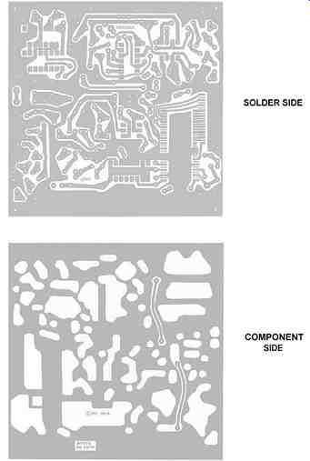
FIG. 3 Solder Side and Component Side of the PC Board for the MPX96
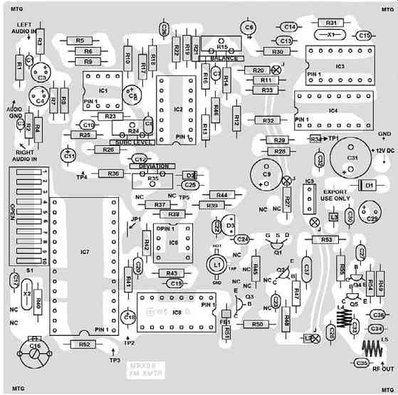 FIG. 4 Parts Layout Diagram of the MPX96 Frequency Synthesized FM Ste
reo Transmitter
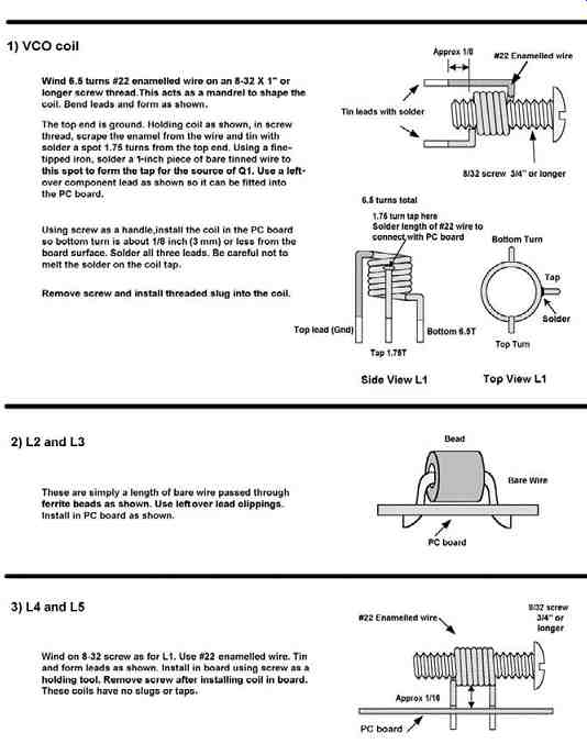
FIG. 5 Coil Data for the MPX96 Frequency Synthesized FM Stereo Transmitter
Construction Procedure
Before beginning construction, familiarize yourself with the PC board and the lay out. Read and understand the circuit description. It makes things a lot easier when you understand what is going on. Obtain all of the parts as detailed in the parts list.
A kit is available from the source mentioned at the end of this section and is recommended because a PC board and all parts on it are included. Use good lighting while assembling your transmitter. A magnifier is also useful. Note that grounded leads of resistors are to be soldered on both sides of the PC board. This task is essential for good grounding. A chip capacitor C21 is also mounted under the PC board. This step will be done later. (See Figures 8-3 through 8-6.)
Except where access may be difficult later, do not solder any connections until as many components as possible are inserted. All coils are installed after components are inserted and soldered in, but this is the only exception. All parts are mounted tight and close to the board, with no exceptions. This step is important for reducing audio noise pickup and for proper operation of the high-speed digital and RF circuits. It also gives a professional appearance to the finished board. Use only rosin core solder, with low residue preferred. Do not use acid core solder or any kinds of paste fluxes. A hot, small, pencil iron is best. (See instructions for chip capacitor mounting in the Appendix. FIG. 5 shows coil fabrication details.)
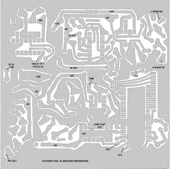
FIG. 6 MPX96 PC Board Solder Side Showing Test Points and Voltages
Do not solder any connections on the bottom of the board until you are instructed to do so. It is best to begin construction by inserting all resistors in the PC board. Make sure that the correct values are inserted. Next, solder all top ground connections. Install all diodes, carefully observing polarity. Next, install all capacitors. Make sure to observe polarity of all electrolytic capacitors. Accidental reversal will cause a malfunction and possibly damage to the circuitry. If you are in doubt about the value or coding of a specific part, measure it if you can. Install all transistors. Some may have preformed leads. Ignore this and, if needed, straighten out the leads for best fit. Make sure the flat side faces the direction shown in the layout. Be careful with Q2 and Q3 because these may be different than preformed leads seem to indicate. If Q2 and Q3 have preformed leads, straighten them with pliers to permit correct orientation. Install trimmer C16 and potentiometers R15, R24, and R35. Pre set C16 to 25 percent capacitance (plates one-quarter meshed). Preset R15, R24, and R25 to halfway (or center). The MPX96 will operate with the initial settings of these trimmers well enough to enable testing and setup. Install the crystals X1 and X2.
Using scissors, trim crystal leads to 3/16ths inch and install. Do not use diagonal cutters because the mechanical snap produced can actually break the crystal elements.
Install ICs, being extremely careful about the correct orientation. If you are a bit squeamish about soldering them and/or having to remove them in the future, you can use low-profile DIP sockets. These are not necessary, but if you prefer to, you can use them. Carefully check all work done so far for accuracy and orientation. Now trim all component leads to length if not done yet, and solder all bottom connections made so far. Do not plug up any unused holes yet. Carefully fabricate coils L1, L4, and L5, and then install them in the PC board. Use an 8-32 screw to hold the coils during the installation procedure. After installing coils, remove the screw and insert the slug fully in coil L1. (Use the coil-winding table for information.) Fabricate the ferrite bead chokes L2 and L3. These are simply wires passed through ferrite beads.
Install them in the PC board. Install C21 (.01 uf chip) on the underside of the PC board. (Refer to the detailed chip mounting instructions in the Appendix.) Carefully inspect all work completed so far. Look for solder shorts, poor joints, missing parts, incorrect parts orientation or placement, and so forth. You are ready to check out the board once everything is satisfactory.
Test and Setup Procedure
Setup and test is simple, but you will need the following items:
- DVM or analog VOM (preferable) 20K/volt or better
- Power supply 13.2 volts DC regulated, low ripple. (Nine AA, or C or D cells connected in series, make a good supply and are recommended if you have no other supply. Do not use a wall-type transformer because these are poorly regulated and may cause bad hum or damage to the circuitry.)
- FM broadcast receiver, stereo with headphones
- CD player, tape deck, or any other line-level stereo audio source
- Stereo patch cable for audio connections
- Clip leads as necessary
The setup procedure is as follows:
1. Carefully inspect the PC board for shorts, missing or wrong parts, IC and transistor orientation, polarity of diodes and electrolytics, and any assembly mistakes, such as missing or poor solder connections.
2. Connect the 13.2-volt power supply to D1 and ground. Connect the positive lead of VOM or DVM set on 1-ampere scale to the positive supply lead; negative meter lead to D1. If your supply has a meter that measures current, the VOM or DVM is not needed. In this case, connect the positive supply lead directly to D1. Connect the negative supply lead to the PC board ground.
Observe the current drawn; this should be about 120 mA. If current is appreciably less (less than 100 mA) or more (more than 140 ma), repeat step 1 because something may be wrong. Nothing should be getting hot, although IC5 normally runs warm after a few minutes. If satisfactory, remove the VOM or DVM from the positive side of supply (if used) and directly connect D1 to the positive supply terminal. Set the VOM or DVM to read voltages of 0-15 volts DC.
3. Connect the negative lead of the VOM or DVM to ground. Check the following voltages, using the positive lead of meter (13.2 volts supply is assumed):
Jct. D1, C34, IC5: 12.6 volts
Pin 16 IC8: 5.0 volts
Pin 3 IC7: 5.0 volts
Collector of Q5: 5.0 volts
Collector of Q4: 1.6 volts
Collector of Q2: 2-3.5 volts
Collector of Q3: 2-3.5 volts
Drain Q1: 8.5 volts
Pin 7 IC6: 8.5 volts Jct. R11, C6, R20: 6.4 volts
Pin 7 IC1: 6.4 volts Pin 1 IC1: 6.4 volts
Pin 16 IC4: 8-10 volts
A variation of 10 percent is normal. Remember to allow for meter accuracy and component and supply voltage variations. If any major variations are noted, repeat step 1.
4. Set S1 (dipswitch) for a frequency of 88.1 MHz, or thereabout if 88.1 MHz is used in your area. If you want to produce even channels, install JP1 and set for 88.0 MHz. Next, connect the DVM or VOM across pins 1 and 4 (polarity does not matter) of IC2 and adjust R15 for a zero voltage reading. Use the lowest scale you can.
5. Tune a nearby FM receiver to 88.1 MHz (88.0 if using even channels) or a close by unused channel if 88.1 MHz is busy in your area. This should be the same frequency as in step 4. Monitor this channel as you proceed.
6. Set the plates of trimmer capacitor C16 at 25 percent mesh and R15, R24, and R35 at center. Set the slug in L1 so it is fully inserted. Connect the VOM or DVM to TP5 (pin 6 of IC6). Listen on the FM receiver. Now start backing out the slug with a nonmetallic screwdriver. Watch the meter. The meter will initially read about 8-9 volts. As you back out the slug further, a point should be reached where the meter reading starts to decrease. At this time, the FM receiver should suddenly quiet down, and you will hear the carrier. As you adjust the slug, the carrier should still be heard in the receiver. Set the slug so the voltage at TP5 is 3-4 volts. The stereo indicator light on the FM receiver should be lit. If not, adjust R35 toward maximum until it lights, then go a little further. The receiver should be quiet. Remove the 13.2-volt supply. The stereo indicator on the receiver should drop out, and the receiver noise should reappear. If everything is correct so far, the next step is to test the unit with an audio signal input.
7. Connect a 12-inch antenna to the RF output J3 (jct. L5 and C35) and apply a stereo audio signal to inputs J1 (left) and J2 (right). Reconnect the DC supply and listen to the FM receiver. You should hear the audio in the receiver.
Adjust R35 to bring the received level to that comparable to other local stations in your area.
8. Confirm stereo operation by connecting audio tone test point TP1 first to the left channel, then the right channel, using a clip lead. The signal should follow in the receiver. Adjust R24 for best separation, as necessary. If R24 seems to have little effect, leave it in the middle position. This completes basic setup, and you can skip to step 13. If you are fussy and have access to test equipment, continue with step 9.
9. Connect a frequency counter to J3 (RF output) and adjust C16 for exactly 88.1000 MHz, or whatever frequency you have programmed.
10. Connect a counter or scope to TP1 and check for a 1187.5-Hz square wave.
This will then verify that the pilot and subcarrier frequencies are 19 and 38 kHz, respectively. You can verify this, too, if you are curious, but it is not necessary.
11. Using a scope connected to TP4, adjust R15 for minimum 38-kHz subcarrier feedthrough. Temporarily kill the 19-kHz pilot by grounding the Jct. of R28, R29, and C12, in order to make this easy to see.
12. Using a sinewave audio generator of 1.5-volts p-p and a frequency of 1000 Hz, check for waveforms shown in FIG. 7 at TP4, with the left, right, and finally both inputs connected to the audio generator. Adjust R24 for best compliance to the figures. Some compromise may be necessary because the optimum setting for the L channel and R channel may be slightly different as a result of normal circuit and component tolerances. Split any residual minor difference between the L and R channels so each has equal error.
13. Set the slug in L1 so that 3 volts are obtained at TP5 at the lowest desired operating frequency (usually 88.1 MHz). Reprogram S1 for around 94.5 MHz and verify that the voltage at TP5 is above 7 volts and still varies with slug setting. This step checks out the synthesizer frequency range. Note that the slug may be almost out of the winding; this is acceptable. Secure it with clear lacquer, cement, hot glue, or a drop of wax.
14. Set up for final desired output frequency. See the programming instructions for more detailed information.
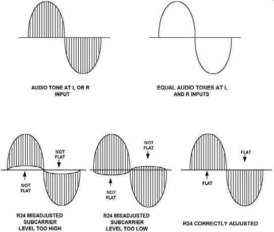
FIG. 7 Waveform at Test Point 4 with a 1 kHz Sine Wave Audio Input
Packaging Considerations
The transmitter may be mounted in almost any case that will accept a PC board of 4-by-4 inches (102-by-102 mm). About 1 inch (25 mm) of height should be allowed.
Either metal or plastic can be used and, because no significant heat is produced, ventilation is not critical, although it is a good idea to allow some airflow if possible.
Make sure that any metal is at least 1/4 inch (6 mm) away from the bottom of the board. If a plastic case is used, it is a good idea to line the bottom of it with copper or aluminum foil to act as a ground plane for the antenna. In addition, a ground bus of some sort is needed with a plastic case. In our prototype, we used a plastic case with removable front and rear panels. The rear panel was removed, and a substitute one was made from ordinary double-sided G-10 PC board stock. This rear panel had the audio input jacks, DC power connector, and RF output jack mounted onto it, and the copper foil was in turn grounded to the main PC board with short wire connections.
This technique enabled very short leads for the audio input connections so no shielding was needed. RCA phono jacks were used for audio connections, a 2.5-mm jack for DC power, and a BNC connector for RF output. Be sure to ground the shell of the RF output connector with a short (1 inch or 25 mm) lead to the ground foil on the PC board. Remember to keep RF leads short, less than 1 inch, as just mentioned.
Audio connectors should be grounded to the audio ground (see layout) and audio leads shielded or kept short to avoid RF pickup and possible distortion. Metal or plastic standoffs can be used to mount the PC board to the case. Antennas can be fashioned from almost any suitable arrangement. We used a replacement cordless phone antenna that collapses to 4 inches (102 mm) and mounted it with epoxy into a BNC male connector, which, with a right-angle fitting, makes a neat, compact antenna. The power supply should be a regulated 13.2-volt DC type. The type commonly sold for powering CB radios and hobby projects should be fine if it has low ripple. Batteries can also be used, but they wear out eventually. For short periods when continuous use is not contemplated, however, batteries are excellent and do not introduce possible hum that can occur with AC-operated supplies. Run-of-the-mill wall-transformer types are definitely not recommended because they are generally poorly regulated and filtered, and excessive voltage that some units may provide can damage the MPX96 circuitry.
Frequency Programming
Frequencies are programmed into the MPX96 by setting 10 DIP switches either closed or open, in a pattern depending on the desired frequency. Each time the frequency is to be changed, these switches must be reset. At first, this process may seem inconvenient, but in practice, there are often only a few available clear channels in the FM broadcast band, and once set, the frequency will probably not be changed often. More than 320 frequencies are possible, and if direct readout is desired, a microprocessor and display are required (the MPX2000, shown in the next section, has this feature). This option is actually not necessary, because once a frequency is chosen, the microprocessor serves no further function. The elimination of the micro processor also greatly reduces the parts count and allows the same money to be spent on better-quality components and circuitry, where it will count toward better RF and audio performance.
Ten DIP switches and one soldered jumper are used for programming. The soldered jumper is used to determine whether odd (88.1, 88.3, 88.5, . . . MHz) channels used in North America, or even (88.0, 88.2, 88.4, ... MHz) channels used in Europe and other parts of the world are to be produced. This setting is determined during construction and is easily changed. This jumper is JP1 and is located on the circuit board near IC7. If JP1 is not installed, odd channels are generated. If JP1 is installed, even channels result. JP1 causes a given DIP switch setting to produce a frequency 100 kHz lower than indicated. So, if 88.4 is desired, install JP1 and use settings for 88.5, and so forth.
To derive the necessary switch pattern, proceed as follows:
1. Choose the desired frequency (e.g., 89.9 MHz).
2. Multiply by 10, or simply remove the decimal point so a whole number between 760 and 1080 results. In our case, this number is 899.
3. Convert this number to binary. This calculation can be performed by the traditional method of successive division by 2, and using the remainders (see a textbook on basic computer science about how to do this) or by looking in a table.
Many math reference books have tables of binary equivalents as well. A table is supplied for 88-93 MHz and several other frequencies as a guide. In between, frequencies can be interpolated.
4. Ignore the least significant digit because this corresponds to JP1 and will be 0 (ground or logical zero) if JP1 is installed, or 1 if not installed (open, high, or logical 1). This corresponds to the logical level of pin 11 of IC7.
5. With the remaining binary number consisting of ones and zeros, set DIP switch position 10 with the first significant digit (0 = closed and 1 = open), set position 9 with the second, position 8 with the third, and so forth until all switches are set. Verify that the frequency generated is correct using a receiver or counter.
6. Check the voltage at TP5 for 3-7 volts DC. Adjust L1 to bring the voltage into this range. If several frequencies are desired, set L1 so that the lowest frequency produces 3 volts at TPA spread of 7-8 percent (depending on circuit tolerances) in frequency is possible without resetting L1. This covers about one-third of the FM broadcast band. In order to reach the highest frequencies (102-108 MHz), it may be necessary to remove the slug in L1. To reach the lowest frequencies (76-MHz region), the slug in L5 must be screwed all the way in. For typical operation in the 88-92 MHz range, the slug may be only about two turns into coil L1. Secure the slug with a drop of cement or wax as previously described. Do not attempt operation above 108 MHz because this range is used by aircraft navigation and communication systems. Interfering with navigational and communications signals in this range could conceivably endanger safety and life or cause an accident.
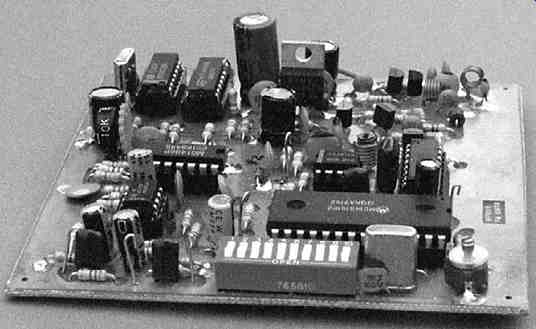
FIG. 8 Completed PC Board of MPX96-The Programming Switch is in the
Fore ground
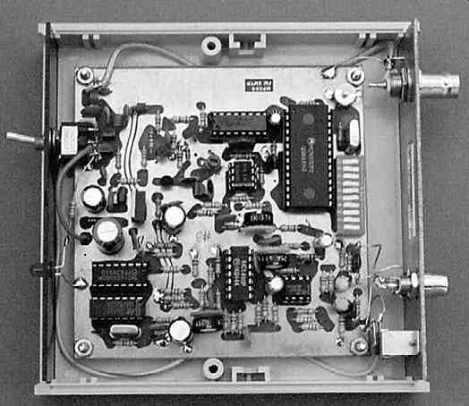
FIG. 9 Top View of the MPX96 Mounted in a Suitable Plastic Case
Applications
The MPX96 is useful anywhere short-range, low-power FM audio links are needed.
It is far superior to free-running FM transmitters and will not drift off channel, and it is perfectly compatible with digitally tuned FM receivers. It is also useful as a teaching aid, unlike low-end units using a BA1404 or other "black box" IC, because it allows access to all MPX signal waveforms and observation of the signal generation process. The circuit is adjustable for optimum performance, and if no test equipment is available, it works well with default settings, so anyone can get satisfactory results with only a VOM or a DVM. In the United States and certain other countries, signal radiation must be kept to a level low enough to not exceed specific field-strength levels and not interfere with other stations using the FM broadcast band.
Check with the applicable laws in your country, such as the FCC or DOT rules and regulations. In the United States, Part 15 of the FCC rules and regulations applies. If you have no easy way to measure field strength, keep the power as low as you can and use only a simple antenna, as short as possible. The MPX96 provides a +10 dBm signal (10 mW) into 50 ohms, running 5 volts on the output amplifier. This power is more than adequate for covering an average property, and only a 12-inch antenna is needed. It is recommended to terminate the output of the transmitter in a 56-ohm resistor, connecting the antenna to the hot side of the termination. This will yield a usable range of 50-200 feet with a typical pocket stereo receiver.
For best results, a relatively clear channel is necessary. The PLL helps tremendously by keeping the signal on frequency. In large metropolitan areas, it may be difficult or impossible to find a clear channel. In this case, try using an in-between channel (i.e., even 100 kHz in the United States and odd 100 kHz in areas using even channel allocations). You might also try to get between two weak stations if possible; however, this can be impossible for digitally tuned receivers, but analog (continuously tuned) receivers will have no problem. Many lower-end pocket stereos are still analog. It is best to operate between 88-92 MHz because this part of the bandwidth is used by lower-powered stations.
Do not set deviation control R35 too high because distortion and interference with other stations may result. Typically, R35 is set at about 75 percent of full open when a typical line-level input (0.5-1.0 volt RMS) signal is fed into J1 and J2. Do not exceed this level because distortion and loss of separation will result. In order to avoid hum, make sure the MPX96 is properly RF grounded, especially if a whip antenna is used.
Operation
Outside the United States For export use, where regulations permit, the voltage on the output buffer can be raised as high as 15 volts, with up to 150 mW output possible, but this output (which is not legal in the United States) is not guaranteed in any way. In this case, a matched antenna should be used and L4 adjusted by compressing or expanding the turns for maximum output. This may allow up to 1 mile or more range, depending on local terrain, if a properly matched antenna is used. Keep the antenna at least 25-30 feet (8-10 meters) from the MPX96 when operating above the 10-mW RF output level because it is possible that stray RF feedback from antenna-to-transmitter circuitry might cause instability and loss of lock in the PLL circuit. Remember, however, that the MPX96 is strictly an entertainment device and is not meant for commercial broadcasting; therefore, no guarantees of any kind can be offered or any technical assistance provided for export use, the details of which must be worked out by the individual user.
Frequency Programming Chart
Note: S1 has 10 rocker switches labeled 1 to 10.
· A "1" corresponds to switch section open (logical 1).
· A "0" corresponds to switch section closed (logical 0).
· S1 sets the logic levels at the programming inputs of IC7.
· Frequencies are shown for U.S. allocations (odd channels), with J1 not installed and pin 11 IC7 at logical 1.
· For operation on even channels, install J1 so pin 11 IC7 is at ground or logical 0. Subtract 0.1 MHz from the frequency indicated in the chart (i.e., 88.1 set tings will produce 88.0, 92.5 will produce 92.4, etc.).
====